JP2012155649A - Semiconductor integrated circuit and bus control method of semiconductor integrated circuit - Google Patents
Semiconductor integrated circuit and bus control method of semiconductor integrated circuit Download PDFInfo
- Publication number
- JP2012155649A JP2012155649A JP2011016223A JP2011016223A JP2012155649A JP 2012155649 A JP2012155649 A JP 2012155649A JP 2011016223 A JP2011016223 A JP 2011016223A JP 2011016223 A JP2011016223 A JP 2011016223A JP 2012155649 A JP2012155649 A JP 2012155649A
- Authority
- JP
- Japan
- Prior art keywords
- signal
- boundary scan
- terminal
- memory controller
- circuit
- Prior art date
- Legal status (The legal status is an assumption and is not a legal conclusion. Google has not performed a legal analysis and makes no representation as to the accuracy of the status listed.)
- Withdrawn
Links
Images




Landscapes
- Debugging And Monitoring (AREA)
Abstract
【課題】ROMエミュレータによるプログラムのデバッグでは、専用のコネクタをCPUが実装された基板に設ける必要ある。このコネクタを追加することにより、配線抵抗が上昇し、メモリのアクセスタイミングを悪化させる。そこで、メモリ間のアクセスタイミングに影響を与えずに、プログラムのデバッグを実現する半導体集積回路を提供する。
【解決手段】半導体集積回路は、メモリに対するアクセスを制御するメモリコントローラと、メモリコントローラの端子と外部端子の間に配置されるバウンダリスキャン回路と、バウンダリスキャン回路の動作モードを決定するモード信号の出力が可能なJTAGインターフェイスと、プログラムのデバッグ時に、モード信号に基づいて、メモリコントローラのリードアクセスを許可する制御信号を、バウンダリスキャン回路を介して、メモリコントローラに発行するタイミング制御回路と、を備える。
【選択図】図1When debugging a program using a ROM emulator, it is necessary to provide a dedicated connector on a board on which a CPU is mounted. By adding this connector, the wiring resistance increases and the access timing of the memory is deteriorated. Therefore, a semiconductor integrated circuit that realizes program debugging without affecting the access timing between memories is provided.
A semiconductor integrated circuit includes a memory controller that controls access to a memory, a boundary scan circuit that is disposed between a terminal of the memory controller and an external terminal, and an output of a mode signal that determines an operation mode of the boundary scan circuit. And a timing control circuit that issues a control signal for permitting read access of the memory controller to the memory controller via the boundary scan circuit based on the mode signal when debugging the program.
[Selection] Figure 1
Description
本発明は、半導体集積回路と半導体集積回路のバス制御方法に関する。特に、プログラムのデバッグ機能を備えた半導体集積回路に関する。 The present invention relates to a semiconductor integrated circuit and a bus control method for the semiconductor integrated circuit. In particular, the present invention relates to a semiconductor integrated circuit having a program debugging function.
組み込み機器に使用する回路は、CPU(Central Processing Unit)として動作する半導体集積回路を備えている。CPUに実行させるプログラムのデバッグには、デバッグのターゲットとなるCPUのソケットにコネクタを挿入し、CPUの機能をコンピュータからエミュレートする方法が存在する。他にも、デバッグのターゲットとなるCPUをそのまま利用し、外部に設けられたメモリ(通常動作時に使用するメモリとは異なるメモリ)上にプログラムをダウンロードしてデバッグを行なうROMエミュレータを使用する方法が存在する。 A circuit used for an embedded device includes a semiconductor integrated circuit that operates as a CPU (Central Processing Unit). For debugging a program to be executed by the CPU, there is a method in which a connector is inserted into a socket of the CPU to be debugged and the function of the CPU is emulated from a computer. Another method is to use a ROM emulator that uses a CPU as a debugging target as it is and downloads a program to an externally provided memory (a memory different from the memory used during normal operation) for debugging. Exists.
非特許文献1にROMを内蔵したROMエミュレータが開示されている。ROMエミュレータを用いたプログラムのデバッグでは、JTAG(Joint Test Action Group)に準拠した手順でCPUとコンピュータが通信し、ROMエミュレータが備えるメモリにアクセスする方法が採用されることが多い。JTAGを用いたデバッグを行なう際には、半導体集積回路の外部端子とCPU間でやり取りされるデータの取得及び設定が必要であり、半導体集積回路(CPU)はバウンダリスキャン回路を備えていることが必要になる。非特許文献2には、バウンダリスキャン回路の構成が開示されている。
Non-Patent Document 1 discloses a ROM emulator incorporating a ROM. In debugging a program using a ROM emulator, a method in which a CPU and a computer communicate with each other according to a procedure compliant with JTAG (Joint Test Action Group) to access a memory included in the ROM emulator is often adopted. When debugging using JTAG, it is necessary to acquire and set data exchanged between the external terminal of the semiconductor integrated circuit and the CPU, and the semiconductor integrated circuit (CPU) may include a boundary scan circuit. I need it. Non-Patent
さらに、特許文献1において、データ書き換えとバウンダリスキャンテストのハードウェアを共用にすることで、基板面積を縮小し、異なる種類の不揮発性メモリの書き換えを行なう半導体装置が開示されている。特許文献1で開示された技術では、バウンダリスキャン回路をプログラム書き換え用のプログラムの一次保存メモリとして使用している。
Further,
また、特許文献2において、コンピュータと拡張ユニット間で授受される複数の信号のうち、所定の信号群をシリアルデータに変換した後に受け渡すと共に、動作速度に直接影響を及ぼす特定の信号を直接受け渡すインターフェイスが開示されている。
Also, in
以下の分析は、本発明の観点からなされたものである。 The following analysis has been made from the viewpoint of the present invention.
上述のように、ROMエミュレータによるデバッグは、CPUが本来使用するメモリとは別のメモリにプログラムをダウンロードして行なわれる。しかし、近年のCPUの動作クロックの高速化は著しく、CPUの動作クロックが高速化すると、CPUとROMエミュレータ間を接続するコネクタの影響が無視できなくなる。 As described above, debugging by the ROM emulator is performed by downloading a program to a memory different from the memory originally used by the CPU. However, the recent increase in CPU operation clock speed is significant, and the influence of the connector connecting the CPU and ROM emulator cannot be ignored when the CPU operation clock speed increases.
図2は、ROMエミュレータを使用したCPUのデバッグシステムの一例を示す図である。図2に示すデバッグシステムについての詳細は後述する。図2に示すデバッグシステムでは、CPU10の本来の動作に必要なプログラムはROM20に格納されており、デバッグの対象となるプログラムはROMエミュレータ2が内蔵するメモリにダウンロードする。プログラムのデバッグ時に、ROM20に格納されたプログラムは使用せず、ROMエミュレータ2が内蔵するメモリにダウンロードしたプログラムを使用する。そのため、デバッグ時には、CPU10と、ROM20及びROMエミュレータ2との接続を切り替えるためのコネクタ40が必要となる。
FIG. 2 is a diagram illustrating an example of a CPU debugging system using a ROM emulator. Details of the debug system shown in FIG. 2 will be described later. In the debugging system shown in FIG. 2, a program necessary for the original operation of the CPU 10 is stored in the
CPU10が実装された基板上に、デバッグ時に限り使用するコネクタ40を追加すると、コネクタ自身が持つ抵抗成分やコネクタを配設することに伴う配線抵抗が上昇し、信号の遅延及び反射を引き起こす。その結果、CPU10からメモリ(ROM20又はROMエミュレータ2が内蔵するメモリ)にアクセスする際のタイミングに対して悪影響を与える。即ち、コネクタ40とコネクタ40を配設するために必要な配線パターンが存在することにより、配線抵抗は上昇し、デバッグ時だけではなく、デバッグ時以外の動作(通常動作)においても、信号の遅延及び反射が発生してしまう。
If the
その結果、CPU10からメモリにアクセスする際にウェイトを挿入するなどの処置が必要であり、CPU10のメモリアクセススピードに関する制約事項となっている。 As a result, a measure such as inserting a wait is required when accessing the memory from the CPU 10, which is a restriction on the memory access speed of the CPU 10.
以上のとおり、従来技術には、解決すべき問題点が存在する。 As described above, there are problems to be solved in the prior art.
本発明の一側面において、メモリに対するアクセスタイミングに影響を与えることなく、プログラムのデバッグを実現する半導体集積回路及び半導体集積回路のバス制御方法が、望まれる。 In one aspect of the present invention, a semiconductor integrated circuit and a bus control method for a semiconductor integrated circuit that can debug a program without affecting the access timing to the memory are desired.
本発明の第1の視点によれば、プログラムの実行が可能な半導体集積回路であって、メモリに対するアクセスを制御するメモリコントローラと、前記メモリコントローラの端子と外部端子の間に配置されるバウンダリスキャン回路と、外部から与えられるJTAG信号に基づき、前記バウンダリスキャン回路の動作モードを決定するモード信号の出力が可能なJTAGインターフェイスと、プログラムのデバッグ時に、前記モード信号に基づいて、前記メモリコントローラのリードアクセスを許可する制御信号を、前記バウンダリスキャン回路に対して出力するタイミング制御回路と、を備え、前記バウンダリスキャン回路は、前記制御信号に基づき、前記メモリコントローラのリードアクセスを許可する半導体集積回路が提供される。 According to a first aspect of the present invention, there is provided a semiconductor integrated circuit capable of executing a program, a memory controller for controlling access to a memory, and a boundary scan arranged between a terminal of the memory controller and an external terminal A JTAG interface capable of outputting a mode signal for determining an operation mode of the boundary scan circuit based on a JTAG signal supplied from the outside, and reading of the memory controller based on the mode signal when debugging a program A timing control circuit that outputs a control signal for permitting access to the boundary scan circuit. The boundary scan circuit is a semiconductor integrated circuit that permits read access to the memory controller based on the control signal. Provided.
本発明の第2の視点によれば、メモリに対するアクセスを制御するメモリコントローラと、前記メモリコントローラの端子と外部端子の間に配置されるバウンダリスキャン回路と、外部から与えられるJTAG信号に基づき、前記バウンダリスキャン回路の動作モードを決定するモード信号の出力が可能なJTAGインターフェイスと、を備え、プログラムの実行が可能な半導体集積回路のバス制御方法であって、プログラムのデバッグ時に、前記バウンダリスキャン回路にデータを設定する工程と、前記モード信号に基づいて、前記メモリコントローラのリード動作を1サイクルの期間許可し、前記メモリコントローラに前記データを読み込ませるデータアップデート工程と、前記データアップデート工程後、前記メモリコントローラのリードサイクルを禁止する工程と、を含む半導体集積回路のバス制御方法が提供される。 According to a second aspect of the present invention, based on a memory controller for controlling access to a memory, a boundary scan circuit disposed between a terminal of the memory controller and an external terminal, and a JTAG signal given from the outside, A JTAG interface capable of outputting a mode signal for determining an operation mode of a boundary scan circuit, and a bus control method for a semiconductor integrated circuit capable of executing a program, wherein the boundary scan circuit is connected to the boundary scan circuit during program debugging. A step of setting data, a data update step of allowing the memory controller to perform a read operation for one cycle based on the mode signal, and causing the memory controller to read the data; and after the data update step, the memory Controller Bus control method for a semiconductor integrated circuit including the step of prohibiting the read cycle, is provided.
本発明の各視点によれば、メモリに対するアクセスタイミングに影響を与えることなく、プログラムのデバッグを実現する半導体集積回路及び半導体集積回路のバス制御方法が、提供される。 According to each aspect of the present invention, there are provided a semiconductor integrated circuit and a semiconductor integrated circuit bus control method that can debug a program without affecting the access timing to the memory.
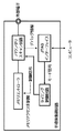
初めに、図1を用いて実施形態の概要について説明する。なお、この概要に付記した図面参照符号は、理解を助けるための一例として各要素に便宜上付記したものであり、本発明を図示の態様に限定することを意図するものではない。 First, the outline of the embodiment will be described with reference to FIG. Note that the reference numerals of the drawings attached to this summary are attached to the respective elements for convenience as an example for facilitating understanding, and are not intended to limit the present invention to the illustrated embodiment.
上述のように、ROMエミュレータを使用するためには、デバッグ時に限り使用するコネクタが必要になる。すると、コネクタが存在しない場合と比較して、CPUを含む基板の配線抵抗が上昇してしまう。その結果、メモリのデータにアクセスするために必要なアドレス信号やデータ信号において、遅延や反射が起きてしまう。そのため、デバッグ時に限らず、通常動作時においても、CPUからメモリにアクセスする際のタイミングを調整することが必要になる。即ち、CPUのメモリアクセススピードに関する制約事項となる。 As described above, in order to use the ROM emulator, a connector used only for debugging is required. As a result, the wiring resistance of the substrate including the CPU increases as compared with the case where no connector is present. As a result, delay and reflection occur in the address signal and data signal necessary for accessing the memory data. Therefore, it is necessary to adjust the timing for accessing the memory from the CPU, not only during debugging but also during normal operation. That is, it becomes a restriction on the memory access speed of the CPU.
そこで、図1に示す半導体集積回路を提供する。図1に示す半導体集積回路は、メモリに対するアクセスを制御するメモリコントローラと、メモリコントローラの端子と外部端子の間に配置されるバウンダリスキャン回路と、外部から与えられるJTAG信号に基づき、バウンダリスキャン回路の動作モードを決定するモード信号の出力が可能なJTAGインターフェイスと、プログラムのデバッグ時に、モード信号に基づいて、メモリコントローラのリードアクセスを許可する制御信号を、バウンダリスキャン回路に対して出力するタイミング制御回路と、を備えている。 Therefore, the semiconductor integrated circuit shown in FIG. 1 is provided. The semiconductor integrated circuit shown in FIG. 1 includes a memory controller that controls access to a memory, a boundary scan circuit disposed between a terminal of the memory controller and an external terminal, and a boundary scan circuit based on a JTAG signal supplied from the outside. A JTAG interface capable of outputting a mode signal for determining an operation mode, and a timing control circuit for outputting a control signal for permitting read access of the memory controller to the boundary scan circuit based on the mode signal when debugging a program And.
プログラムのデバッグ時は、バウンダリスキャン回路を介してCPUからメモリに対するアクセス情報をコンピュータに取り込み、コンピュータ上でエミュレーションした結果をバウンダリスキャン回路からメモリコントローラに設定する。その際に、メモリコントローラのリードアクセスを制限しなければ、コンピュータ上でエミュレーションを実行する前にデータの取得動作(データのフェッチ)が発生してしまう。そこで、デバッグ時におけるメモリコントローラのメモリに対するアクセスを制限し、コンピュータ上でエミュレーションしたデータが設定可能となった後に、メモリコントローラにおけるリードアクセスを許可することとした。即ち、デバッグ時にはメモリコントローラは常時、ウェイト状態とする。そして、コンピュータによるエミュレーション結果が準備できた後に、エミュレーション結果をバウンダリスキャン回路に設定する。その後、エミュレーション結果をメモリコントローラに読み込ませる指示がJTAGインターフェイスから発行され、JTAGインターフェイスはモード信号としてタイミング制御回路に出力する。タイミング制御回路では、モード信号からメモリコントローラに対してリードサイクルを許可する制御信号を発行し、制御信号を受け付けたバウンダリスキャン回路はメモリコントローラのリードアクセスを許可する。 When debugging a program, access information to the memory from the CPU is fetched into the computer via the boundary scan circuit, and the result of emulation on the computer is set from the boundary scan circuit to the memory controller. At this time, if the read access of the memory controller is not restricted, a data acquisition operation (data fetch) occurs before the emulation is executed on the computer. Therefore, the memory controller's access to the memory at the time of debugging is restricted, and after the data emulated on the computer can be set, read access in the memory controller is permitted. That is, the memory controller is always in a wait state during debugging. Then, after the computer emulation result is prepared, the emulation result is set in the boundary scan circuit. Thereafter, an instruction to read the emulation result into the memory controller is issued from the JTAG interface, and the JTAG interface outputs the mode signal to the timing control circuit. In the timing control circuit, a control signal for permitting a read cycle is issued from the mode signal to the memory controller, and the boundary scan circuit receiving the control signal permits read access of the memory controller.
その結果、図1に示す半導体集積回路に実行させるプログラムのデバッグの際は、デバッグの対象となっているプログラムをコンピュータ上に記憶することが可能となり、ROMエミュレータ等のデバッグには不可欠であったコネクタを削除することが可能になる。デバッグ時に限り必要となるコネクタが存在することで発生していた信号の遅延や反射を抑制することが可能になり、デバッグ機能の実現を目的としたメモリアクセスのタイミング調整は不要となる。そのため、CPUのメモリアクセススピードに関する制約を解消することができる。 As a result, when debugging a program to be executed by the semiconductor integrated circuit shown in FIG. 1, the program to be debugged can be stored on a computer, which is indispensable for debugging a ROM emulator or the like. It becomes possible to delete the connector. It is possible to suppress signal delays and reflections that have occurred due to the presence of connectors that are required only during debugging, and it is not necessary to adjust the timing of memory access for the purpose of realizing a debugging function. Therefore, it is possible to eliminate restrictions on the memory access speed of the CPU.
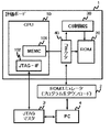
次に、図2に示すROMエミュレータを使用したCPUのデバッグシステムについて説明する。図2に示すデバッグシステムは、評価ボード1と、ROMエミュレータ2と、JTAGマスタ3と、PC(Personal Computer)4から構成されている。評価ボード1は、CPU10と、ROM20と、CS制御器30と、コネクタ40から構成されている。
Next, a CPU debugging system using the ROM emulator shown in FIG. 2 will be described. The debugging system shown in FIG. 2 includes an
CPU10は、中央演算装置(CPU)として動作する半導体集積回路である。CPU10は、CPU10に接続されているメモリに対するアクセスを制御するメモリコントローラ(以下、MEMCと呼ぶ)101と、JTAGに準拠した通信信号のインターフェイスとなるJTAG−IF102を備えている。CPU10のMEMC101と、ROM20又はROMエミュレータ2が内蔵するメモリはコネクタ40を介して接続されている。
The CPU 10 is a semiconductor integrated circuit that operates as a central processing unit (CPU). The CPU 10 includes a memory controller (hereinafter referred to as MEMC) 101 that controls access to a memory connected to the CPU 10 and a JTAG-
ROM20には、CPU10に実行させるプログラムが格納されている。但し、ROM20には、デバッグ時にはターゲットとなるプログラムは格納されていない。
The
CS制御器30は、CPU10にROM20に格納したプログラムを実行させるときは、CPU10が供給するCS(Chip Select)信号をROM20に供給し、デバッグ時にはROMエミュレータ2にCS信号を供給する。従って、デバッグ時にはCPU10はコネクタ40を経由して、ROMエミュレータ2が内蔵するメモリにアクセスする。
The
コネクタ40は、CPU10とROM20を接続するバスに設けられており、さらにCPU10とROMエミュレータ2を接続する。上述のように、ROMエミュレータ2が内蔵するメモリにデバッグのターゲットとなるプログラムをダウンロードする。なお、ROMエミュレータ2が内蔵するメモリの書き換え(プログラムのダウンロード)はPC4から行なう。また、CPU10はJTAGマスタ3を介することで、JTAGに準拠した手順でPC4と通信する。
The
図2に示すデバッグシステムでは、デバッグのターゲットとなるプログラムをROMエミュレータ2が内蔵するメモリにダウンロードし、CPU10におけるプログラムの実行・停止などの制御はJTAGマスタ3を介してPC4から行なう。その際に、CPU10とROMエミュレータ2が内蔵するメモリ間でやり取りされるデータの取得や、CPU10に対して任意のデータが設定できることが必要になる。そのため、CPU10にはバウンダリスキャン回路が内蔵されている。
In the debug system shown in FIG. 2, a program to be debugged is downloaded to a memory built in the
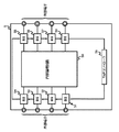
次に、バウンダリスキャン回路について説明する。図3は、非特許文献2で開示されているバウンダリスキャン回路を備える半導体集積回路5の一構成例を示す図である。
Next, the boundary scan circuit will be described. FIG. 3 is a diagram illustrating a configuration example of the semiconductor integrated circuit 5 including the boundary scan circuit disclosed in
図3に示す半導体集積回路5は、内部論理回路50と、バウンダリスキャンレジスタ51乃至58と、TAP(Test Access Port)コントローラ59から構成されている。バウンダリスキャンレジスタ51乃至58とTAPコントローラ59によって、バウンダリスキャン回路を構成している。
The semiconductor integrated circuit 5 shown in FIG. 3 includes an
図3に示すバウンダリスキャン回路は、半導体集積回路5の外部端子と内部論理回路50の間でやり取りされるデータの取得及び任意なデータの設定を可能にするためのものである。半導体集積回路5には、外部端子と内部論理回路50の間にバウンダリスキャンレジスタ51乃至58が設けられている。なお、バウンダリスキャンレジスタ51乃至58は、それぞれ直列に接続されており、各バウンダリスキャンレジスタが保持するデータを順次、次段のバウンダリスキャンレジスタに出力可能となっている(シフトレジスタを構成している)。
The boundary scan circuit shown in FIG. 3 is for enabling acquisition of data exchanged between the external terminal of the semiconductor integrated circuit 5 and the
TAPコントローラ59がバウンダリスキャンレジスタ51乃至58の制御を行なう。例えば、各バウンダリスキャンレジスタでのデータの取り込みや、取り込んだデータを次段のバウンダリスキャンレジスタにシフトアウトする動作をTAPコントローラ59が制御する。
The
続いて、バウンダリスキャンレジスタについて説明する。図4は、非特許文献2において開示されたバウンダリスキャンレジスタの一構成例である。図4に示すバウンダリスキャンレジスタは、双方向のデータの入出力が可能であり、マルチプレクサ60乃至64と、フリップフロップ65及び66と、バッファ67により構成されている。なお、マルチプレクサ60乃至64に記したH及びLは、入力切り替え信号がHレベルの際に選択される入力端と、Lレベルの際に選択される入力端を示すものである(以下の説明においても同様とする)。
Next, the boundary scan register will be described. FIG. 4 is a configuration example of the boundary scan register disclosed in
図2に示す構成を持つデバッグシステムでは、ROMエミュレータが内蔵するメモリにデバッグのターゲットとなるプログラムをダウンロードする。そのため、プログラムのデバッグを行なうためには、CPU10とROMエミュレータ2を接続するためのコネクタ40が必要となる。さらに、CPU10が出力するCS信号を切り替えるためのCS制御器30も必要である。
In the debugging system having the configuration shown in FIG. 2, a program to be debugged is downloaded to a memory built in the ROM emulator. Therefore, in order to debug a program, a
これらのデバッグ時に限り必要なコネクタ40やCS制御器30を追加することにより、CPU10と、ROM20又はROMエミュレータ2が内蔵するメモリまでの配線抵抗が上昇する。その結果、メモリにアクセスする際に用いるアドレス信号やデータ信号が遅延、反射するといった問題が起こる。この信号の遅延及び反射は、通常動作時(デバッグ時以外)においても発生する。そのため、CPU10からメモリにアクセスする際にはウェイトを挿入するなどの処置が必要であり、CPU10のメモリアクセススピードが低下する要因となる。
By adding the
[第1の実施形態]
次に、本発明の第1の実施形態について、図面を用いてより詳細に説明する。図5は、本実施形態に係る半導体集積回路(CPU)を含むデバッグシステムの一構成例を示す図である。図5において、図2と同一の構成要素には、同一の符号を表し、その説明を省略する。
[First Embodiment]
Next, the first embodiment of the present invention will be described in more detail with reference to the drawings. FIG. 5 is a diagram illustrating a configuration example of a debug system including a semiconductor integrated circuit (CPU) according to the present embodiment. In FIG. 5, the same components as those in FIG. 2 are denoted by the same reference numerals, and the description thereof is omitted.
図5に示すデバッグシステムは、評価ボード7と、JTAGマスタ3と、PC4から
構成されている。PC4には、デバッグのターゲットとなるプログラムが格納されている。評価ボード7は、CPU70とROM20から構成されている。
The debug system shown in FIG. 5 includes an evaluation board 7, a
CPU70は、MEMC101と、JTAG−IF102と、タイミング制御回路103を備え、中央演算装置として動作する半導体集積回路である。図2に示すデバッグシステムと図5に示すデバッグシステムとを比較すると、評価ボード7にはCS制御器30及びコネクタ40は存在しないことが分かる。
The
図6は、CPU70の内部構成の一例を示す図である。図6に示すCPU70は、MEMC101と、JTAG−IF102と、タイミング制御回路103と、バウンダリスキャンレジスタ104乃至106から構成されている。MEMC101は、バウンダリスキャンレジスタ106を介してCPU70のアドレス/コマンド端子と接続されている。同様に、MEMC101はバウンダリスキャンレジスタ105を介してデータ端子、バウンダリスキャンレジスタ104を介してウェイト端子と、それぞれ接続されている。なお、CPU70のアドレス/コマンド端子、データ端子、ウェイト端子は、それぞれROM20のアドレス端子、データ端子、ウェイト端子と接続されている。
FIG. 6 is a diagram illustrating an example of the internal configuration of the
また、ROM20がウェイト端子をウェイト状態にしている間は、MEMCからROM20に対してメモリアクセスは行なわれない。なお、図5に示すデバッグシステムでは、デバッグ時のウェイト端子の状態を基板上に設けたスイッチなどを使用して常にLレベルに設定する。
In addition, while the
タイミング制御回路103は、MEMC101から基準クロックとなるCPU_CLKを受け付け、JTAG−IF102からSelectA信号を受け付ける。SelectA信号は上述のモード信号に相当する。タイミング制御回路103は、SelectB信号をバウンダリスキャンレジスタ104乃至106に出力する。SelectB信号は上述の制御信号に相当する。
The
JTAG−IF102は、バウンダリスキャンレジスタ104にScan_In1信号を出力し、バウンダリスキャンレジスタ104乃至106に対してShift信号を出力する。また、JTAG−IF102から、バウンダリスキャンレジスタ104乃至106に対してクロック(JTAG_CLK)を出力する。
The JTAG-
なお、バウンダリスキャンレジスタ104乃至106に入力するScan_In信号は、Scan_In1、Scan_In2、Scan_In3と表記する。同様に、バウンダリスキャンレジスタ104乃至106から出力するScan_Out信号は、Scan_Out1、Scan_Out2、Scan_Out3と表記する。 Note that the Scan_In signals input to the boundary scan registers 104 to 106 are represented as Scan_In1, Scan_In2, and Scan_In3. Similarly, the Scan_Out signals output from the boundary scan registers 104 to 106 are represented as Scan_Out1, Scan_Out2, and Scan_Out3.
次に、バウンダリスキャンレジスタ104乃至106の構成について説明する。なお、バウンダリスキャンレジスタ104乃至106の構成は同一のため、バウンダリスキャンレジスタ104に限り説明を行なう。図7は、バウンダリスキャンレジスタ104の内部構成の一例を示す図である。
Next, the configuration of the boundary scan registers 104 to 106 will be described. Since the configuration of the boundary scan registers 104 to 106 is the same, only the
バウンダリスキャンレジスタ104は、マルチプレクサ1041及び1042と、フリップフロップ1043から構成される。CPU70のウェイト端子は、マルチプレクサ1041の入力端子に接続され、フリップフロップ1043の出力端子はマルチプレクサ1041の他の入力端子に接続される。マルチプレクサ1041の出力端子は、MEMC101の入力端子及びマルチプレクサ1042の入力端子に接続される。マルチプレクサ1041の出力する信号は、SelectB信号に基づいて定まる。マルチプレクサ1042には、マルチプレクサ1041の出力に加えてScan_In1信号が入力される。また、マルチプレクサ1042の出力する信号は、Shift信号に基づいて定まる。マルチプレクサ1042の出力端子はフリップフロップ1043の入力端子に接続される。フリップフロップ1043の出力端子は、マルチプレクサ1041の入力端子と接続されると共に、バウンダリスキャンレジスタ104のScan_Out1信号として、次段のフリップフロップ105に出力される。
The
続いて、タイミング制御回路103の詳細な構成について説明する。図8は、タイミング制御回路103の内部構成の一例を示す図である。
Next, a detailed configuration of the
タイミング制御回路103は、フリップフロップ1031乃至1033と、AND回路1034から構成されている。JTAG−IF102が出力するSelectA信号をフリップフロップ1031のデータ入力端子で受け付ける。フリップフロップ1031の出力端子は、フリップフロップ1032のデータ入力端子及びAND回路1034の入力端子に接続される。さらに、AND回路1034の他の入力端子はフリップフロップ1032の反転出力端子と接続される。AND回路1034の出力端子はフリップフロップ1033のデータ入力端子に接続される。フリップフロップ1033の出力端子から、SelectB信号を出力する。なお、フリップフロップ1031乃至1033のクロック端子には、MEMC101が供給するCPU_CLKが入力される。
The
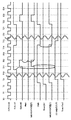
図9は、メモリアクセスの1サイクルがCPU_CLKの1周期に等しいとした場合のタイミング制御回路103の動作を示す図である。図9の縦軸には、CPU_CLK、SelectA信号、フリップフロップ1031の出力、フリップフロップ1032の反転出力、AND回路1034の出力、SelectB信号を示す。
FIG. 9 is a diagram illustrating the operation of the
時刻T0〜T2の期間に入力されるSelectA信号はLレベルであるので、フリップフロップ1031の出力及びAND回路1034の出力はLレベルとなる。フリップフロップ1032の反転出力はHレベルとなる。その後、時刻T2とT3の期間において、SelectA信号がHレベルに変化したものとする。その結果、時刻T3において、フリップフロップ1031の出力はHレベルとなる。同時に、AND回路1034の出力もHレベルとなる。すると、フリップフロップ1032の出力は1クロック遅延して反転されるので、時刻T4においてLレベルとなる。フリップフロップ1032の反転出力を受け付けたAND回路1034の出力は、時刻T4においてLレベルとなる。
Since the SelectA signal input during the period of time T0 to T2 is at the L level, the output of the flip-
このように、AND回路1034の出力は時刻T3とT4の期間に限りHレベルを出力する。そして、フリップフロップ1033はAND回路1034の出力をCPU_CLKに同期させ、SelectB信号として1クロック遅延させて出力する。
In this way, the output of the AND
一方、時刻T7とT8の期間においてSelectA信号がLレベルに遷移したとすると、フリップフロップ1031の出力はLレベルとなる。フリップフロップ1031の出力がLレベルとなると、フリップフロップ1032の反転出力は時刻T9においてHレベルとなる。時刻T9における各信号の状態は時刻T0の状態と同じであり、時刻T9以降は上述の動作を繰り返す。
On the other hand, if the SelectA signal transits to the L level during the period of time T7 and T8, the output of the flip-
次に、本実施系形態に係るCPU70を含むデバッグシステムの動作について説明する。図10は、CPU70を含むデバッグシステムによってデバッグを行なう際の動作の概略を示す図である。
Next, the operation of the debug system including the
ステップS01では、CPU70の内部からMEMC101に対してアドレスを指定したデータの取り込み指示が出力される。その指示を受けたMEMC101は、指定されたアドレス信号をバウンダリスキャンレジスタ106に対して出力する。
In step S01, an instruction to fetch data specifying an address is output from the
ステップS02では、バウンダリスキャンレジスタ104乃至106で保持しているデータをPC4に取り込む。本ステップでは、各バウンダリスキャンレジスタで保持したデータを次段のバウンダリスキャンレジスタに順次送り、PC4において最終段のバウンダリスキャンレジスタ(バウンダリスキャンレジスタ106)から出力されるデータを順次取り込む。ここで、バウンダリスキャンレジスタ104乃至106でデータの取り込みを行なう動作をバウンダリスキャンレジスタのキャプチャーモードと呼び、各バウンダリスキャンレジスタで保持したデータを次段のバウンダリスキャンレジスタに順次送る動作をバウンダリスキャンレジスタのスキャンシフトモードと呼ぶ。 In step S02, the data held in the boundary scan registers 104 to 106 is taken into the PC 4. In this step, the data held in each boundary scan register is sequentially sent to the next-stage boundary scan register, and the data output from the last-stage boundary scan register (boundary scan register 106) is sequentially fetched in the PC4. Here, the operation of capturing data in the boundary scan registers 104 to 106 is called the capture mode of the boundary scan register, and the operation of sequentially transmitting the data held in each boundary scan register to the boundary scan register of the next stage is performed in the boundary scan register. This is called a scan shift mode.
ステップS03では、PC4において、取り込んだアドレス信号を基にROMデータのエミュレートを行なう。さらに、エミュレート結果を返答データとして生成する。 In step S03, the ROM data is emulated in the PC 4 based on the fetched address signal. Further, the emulation result is generated as response data.
ステップS04では、ステップS03で生成した返答データをバウンダリスキャンレジスタ104乃至106に設定する。 In step S04, the response data generated in step S03 is set in the boundary scan registers 104 to 106.
ステップS05では、バウンダリスキャンレジスタ104乃至106に設定した返答データをMEMC101に読み込ませる。ここで、バウンダリスキャンレジスタに設定したデータをMEMCに読み込ませる動作をバウンダリスキャンレジスタのアップデートモードと呼ぶ。
In step S05, the response data set in the boundary scan registers 104 to 106 is read into the
ステップS05が終了すると、ステップS01に遷移し、プログラムのデバッグを継続する。 When step S05 ends, the process proceeds to step S01, and debugging of the program is continued.
続いて、図10の各ステップにおけるCPU70の動作について説明する。図11は、CPU70の各信号の動作を示すタイミングチャートである。図11の縦軸には、CPU_CLK、SelectA信号、SelectB信号、ウェイト信号(ウェイト端子の状態)、マルチプレクサ1041の出力、Shift信号、Scan_In1信号、マルチプレクサ1042の出力、フリップフロップ1043の出力、Scan_Out1信号を示す。
Subsequently, the operation of the
時刻T0〜T2の期間は、上述のキャプチャーモードに相当する。時刻T0〜T2の期間においては、JTAG−IF102が出力するSelectA信号がLレベルであるため、タイミング制御回路103が出力するSelectB信号もLレベルである。すると、マルチプレクサ1041はウェイト端子の状態を出力し、ウェイト端子の状態はLレベルであるので、マルチプレクサ1041の出力はLレベルとなる。バウンダリスキャンレジスタ104の出力としてLレベルを受け取ったMEMC101では、CPU70の外部端子であるウェイト端子がLレベルであると解釈し、メモリに対するアクセスを行なわない(中断する)。また、Shift信号がLレベルであれば、マルチプレクサ1042はマルチプレクサ1041の出力(Lレベル)を選択し、フリップフロップ1043に出力する。フリップフロップ1043では、入力された信号(Lレベル)をScan_Out1信号として次段のバウンダリスキャンレジスタ105に出力する。このようにして、バウンダリスキャンレジスタ104で保持するウェイト信号の値を次段のバウンダリスキャンレジスタ105及びMEMC101に対して出力する。
The period from time T0 to T2 corresponds to the capture mode described above. In the period from time T0 to time T2, the SelectA signal output from the JTAG-
図12は、キャプチャーモード時のバウンダリスキャンレジスタ104の信号フローを示した図である。図12において、点線がキャプチャーモード時に選択されている信号の経路である。図12からも明らかなように、バウンダリスキャンレジスタ104ではウェイト信号をMEMC101に伝えると共に、フリップフロップ1043で保持した情報を次段のバウンダリスキャンレジスタ105に出力する。
FIG. 12 is a diagram illustrating a signal flow of the
次に、スキャンシフトモードについて説明する。図11の時刻T2〜T3の期間は、上述のスキャンシフトモードに相当する。スキャンシフトモードでは、CPU70の外部から入力される信号をMEMC101に伝えながら、前段のバウンダリスキャンレジスタが出力するデータを次段のバウンダリスキャンレジスタに伝える(シフトする)。時刻T2〜T3の期間においても、SelectB信号はLレベルであるのでウェイト信号はMEMC101に伝えられる。しかし、スキャンシフトモードでは、マルチプレクサ1042が受け付けるShift信号がHレベルとなるので、Scan_In1信号が選択されて後段のフリップフロップ1043に出力する。そして、フリップフロップ1043では、JTAG−IF102が供給するJTAG_CLKに同期してScan_Out1信号として、Scan_In1信号を出力する。このように、バウンダリスキャンレジスタ104乃至106が取り込んだデータを次段のバウンダリスキャンレジスタに出力することで、最終的にPC4において、MEMC101が出力するアドレス信号やCPU70のデータ端子やウェイト端子の状態(信号)を取り込むことができる。
Next, the scan shift mode will be described. A period from time T2 to time T3 in FIG. 11 corresponds to the above-described scan shift mode. In the scan shift mode, a signal input from the outside of the
図13は、図12と同様、スキャンシフトモード時のバウンダリスキャンレジスタ104の信号フローを示したものである。
FIG. 13 shows the signal flow of the
次に、アップデートモードについて説明する。図11の時刻T10〜T12の期間は、上述のアップデートモードに相当する。アップデートモードでは、バウンダリスキャンレジスタ104乃至106で形成するバウンダリスキャン回路に設定されたデータ(返答データ)をMEMC101に読み込ませる。アップデートモードでは、Shift信号はHレベルであり、マルチプレクサ1042の出力はScan_In1信号が選択されて出力される。すると、Scan_In1信号にHレベルが設定されている場合には、フリップフロップ1043を介してマルチプレクサ1041にHレベルが出力される。
Next, the update mode will be described. The period from time T10 to time T12 in FIG. 11 corresponds to the update mode described above. In the update mode, the data (response data) set in the boundary scan circuit formed by the boundary scan registers 104 to 106 is read into the
一方、タイミング制御回路103では、時刻T10とT11の期間にSelectA信号がLレベルからHレベルに変化しているため、この変化に基づいてSelectB信号が時刻T11とT12の期間に限りHレベルとなる。マルチプレクサ1041では、時刻T11とT12の期間に限り、フリップフロップ1043の出力を選択して出力する。この場合には、Scan_In1信号にHレベルが設定されているため、MEMC101では、Scan_In1信号のHレベルを1クロックの期間受け付ける。
On the other hand, in the
バウンダリスキャンレジスタ104の出力(マルチプレクサ1041の出力)は、MEMC101においてはウェイト信号と解釈され、ウェイト信号がHレベルに変化したと認識される。その結果、MEMC101ではウェイトが解除されメモリアクセス(データの取り込み)が実行される。従って、JTAG−IF102が、PC4でエミュレーションしたデータ(返答データ)を時刻T11までにバウンダリスキャンレジスタ104乃至106に設定することで、返答データをMEMC101に読み込ませることが可能になる。
The output of the boundary scan register 104 (the output of the multiplexer 1041) is interpreted as a wait signal in the
さらに、タイミング制御回路103が出力するSelectB信号は時刻T12ではLレベルとなるのでマルチプレクサ1041の出力はウェイト端子の状態を出力することになる。ウェイト端子の状態はLレベルであるので、MEMC101によるメモリアクセスは再び中断される。以上の動作で、図10におけるステップS05まで終了したことになる。その後は、ステップS01に戻り次のエミュレーションが実行される。具体的には、時刻T14において、JTAG−IF102からSelectA信号としてLレベルが出力され、時刻T21までの間にPC4にデータが取り込まれる。その後、時刻T21とT22の間にSelectA信号をHレベルとすることで、SelectB信号が1サイクル間に限りHレベルとなり、MEMC101にデータを読み取らせることが可能になる。
Further, since the SelectB signal output from the
図14は、図12と同様、アップデートモード時のバウンダリスキャンレジスタ104の信号フローを示したものである。
FIG. 14 shows the signal flow of the
以上のように、バウンダリスキャン回路を内蔵する半導体集積回路において、タイミング制御回路103を設け、メモリコントローラ(MEMC101)に供給するウェイト信号を適宜、制御することでプログラムのデバッグを行なうことができる。ウェイト信号を適切に制御しなければ、MEMC101はメモリに対してアクセス可能と解釈するためバウンダリスキャンレジスタによるアップデートモードが終了すると即座にデータのフェッチを始めてしまう。
As described above, in the semiconductor integrated circuit including the boundary scan circuit, the
図11のタイミングを例に取ると、時刻T12で再びウェイト信号をLレベルとしてMEMC101に出力しなければ、MEMCではメモリに対してアクセス可能と判断し、次々とデータのフェッチを始めてしまう。しかし、デバッグ時にはPC4においてプログラムのエミュレーションをしなければならず、時刻T12の後、即座にデータの用意はできない。そこで、MEMC101に対するウェイト信号はLレベルを基本として、必要に応じてタイミング制御回路103によって制御する。
Taking the timing of FIG. 11 as an example, if the wait signal is not again output to the
ROMエミュレータによるデバッグでは、専用のコネクタが必要であったが、本実施形態に係る半導体集積回路を含むデバッグシステムであれば専用のコネクタは必要ない。ROMエミュレータを使ったデバッグ方法では、コネクタ等の追加配線の影響で信号が遅延してしまい、追加配線の遅延を考慮しなければ、データを正しく読み出すことができないという問題が発生していた。この問題を解決するためには、メモリにアクセスするタイミングを変更(余分なウェイトを挿入など)するなどの対処が必要であった。 In the debugging by the ROM emulator, a dedicated connector is necessary. However, if the debugging system includes the semiconductor integrated circuit according to the present embodiment, the dedicated connector is not necessary. In the debugging method using the ROM emulator, the signal is delayed due to the influence of the additional wiring such as the connector, and there is a problem that the data cannot be read correctly unless the delay of the additional wiring is taken into consideration. In order to solve this problem, it is necessary to take measures such as changing the timing of accessing the memory (such as inserting an extra wait).
しかし、本実施形態に係る半導体集積回路を含むデバッグシステムにおいては、バウンダリスキャンレジスタを経由して、直接データを読み取り、その読み取ったデータからMEMC101に返答するデータを作成し、MEMC101に読み込ませるという動作をさせるため、メモリのアクセスタイミングを調整する必要はないという効果を有する。
However, in the debug system including the semiconductor integrated circuit according to the present embodiment, an operation is performed in which data is directly read via the boundary scan register, data to be returned to the
また、プログラムのデバッグ時に限り必要であったコネクタ等が不要であり、本実施形態に係る半導体集積回路を備えた製品のコストダウンを実現できる。 Further, a connector or the like that is necessary only when debugging a program is unnecessary, and the cost of a product including the semiconductor integrated circuit according to the present embodiment can be reduced.
[第2の実施形態]
続いて、第2の実施形態について図面を参照して詳細に説明する。
[Second Embodiment]
Next, a second embodiment will be described in detail with reference to the drawings.
本実施形態に係る半導体集積回路(CPU)は、リードアクセスサイクル中であることを示す信号の出力が可能なMEMC101aを備えているものとする。リードアクセスサイクル中であることを示す信号(アクセス通知信号)をRDZ信号と定め、RDZ信号がLレベルであればMEMC101aがリードサイクル中であることを示すものとする。 The semiconductor integrated circuit (CPU) according to the present embodiment includes a MEMC 101a that can output a signal indicating that a read access cycle is in progress. A signal (access notification signal) indicating that a read access cycle is in progress is defined as an RDZ signal. If the RDZ signal is at L level, it indicates that the MEMC 101a is in a read cycle.
図15は、本実施形態に係るCPU70aが備えるタイミング制御回路103aの一構成例を示す図である。図15に示すタイミング制御回路103aは、AND回路1035とインバータ1036から構成されている。
FIG. 15 is a diagram illustrating a configuration example of the timing control circuit 103a included in the CPU 70a according to the present embodiment. The timing control circuit 103a shown in FIG. 15 includes an AND
MEMC101aが出力するRDZ信号をインバータ1036に入力し、インバータ1036の出力端子をAND回路1035の入力端子に接続する。また、JTAG−IF102が出力するSelectA信号をAND回路1035の他の入力端子により受け付ける。なお、第1の実施形態に係るCPU70と本実施形態に係るCPU70aの相違点は、MEMC101aとタイミング制御回路103aであり、他の説明は省略する。
The RDZ signal output from the MEMC 101a is input to the
図16は、タイミング制御回路103aの動作を示す図である。図16の縦軸には、CPU_CLK、MEMC101aの出力するRDZ信号、SelectA信号、インバータ1036の出力、SelectB信号を示す。図16のRDZ信号は、時刻T1にLレベルに変化し、時刻T9とT10の期間内でHレベルに変化している。この間はMEMC101aによるリードサイクルが継続していることを意味する。そして、JTAG−IF102の出力するSelectA信号が時刻T3でHレベルと変化している。すると、AND回路1035にはインバータ1036の出力するHレベルとSelectA信号のHレベルが入力されることになるため、SelectB信号は時刻T3でHレベルに変化する。その後、RDZ信号がHレベルに変化(リードアクセスサイクルが終了)すると同時にSelectB信号はLレベルに変化する。
FIG. 16 is a diagram illustrating the operation of the timing control circuit 103a. The vertical axis in FIG. 16 indicates CPU_CLK, the RDZ signal output from the MEMC 101a, the SelectA signal, the output of the
このように、SelectB信号はMEMC101aの1回のリードアクセス中に限りHレベルとなる。即ち、JTAG−IF102から各バウンダリスキャンレジスタで保持するデータをMEMC101aに取り込ませることを目的としてSelectA信号がHレベルに設定され、かつ、MEMC101aのリードアクセスサイクルが継続している期間(RDZ信号がLレベルの期間)に限りSelectB信号がHレベルに設定される。その結果、バウンダリスキャンレジスタによるアップデートモードが実現できる。タイミング制御回路103aが生成するSelectB信号以降の動作は、第1の実施形態に係るCPU70の動作と同様のため省略する。
Thus, the SelectB signal becomes H level only during one read access of the MEMC 101a. In other words, the SelectA signal is set to the H level for the purpose of causing the MEMC 101a to capture the data held in each boundary scan register from the JTAG-
以上のように、MEMC101aがRDZ信号の出力が可能であれば、タイミング制御回路103aを簡易な構成とすることができる。 As described above, if the MEMC 101a can output the RDZ signal, the timing control circuit 103a can have a simple configuration.
なお、上記の特許文献等の各開示を、本書に引用をもって繰り込むものとする。本発明の全開示(請求の範囲を含む)の枠内において、さらにその基本的技術思想に基づいて、実施形態の変更・調整が可能である。また、本発明の請求の範囲の枠内において種々の開示要素の多様な組み合わせないし選択が可能である。すなわち、本発明は、請求の範囲を含む全開示、技術的思想にしたがって当業者であればなし得るであろう各種変形、修正を含むことは勿論である。例えば、第1及び第2の実施形態では、バウンダリスキャンレジスタは片方向タイプのスキャン回路として説明したが、図4に示すような双方向タイプを採用することも可能である。 It should be noted that the disclosures of the above patent documents and the like are incorporated herein by reference. Within the scope of the entire disclosure (including claims) of the present invention, the embodiment can be changed and adjusted based on the basic technical concept. Various combinations and selections of various disclosed elements are possible within the scope of the claims of the present invention. That is, the present invention of course includes various variations and modifications that could be made by those skilled in the art according to the entire disclosure including the claims and the technical idea. For example, in the first and second embodiments, the boundary scan register has been described as a one-way type scan circuit, but a bidirectional type as shown in FIG. 4 may be employed.
1、7 評価ボード
2 ROMエミュレータ
3 JTAGマスタ
4 PC
5 半導体集積回路
10、70、70a CPU
20 ROM
30 CS制御器
40 コネクタ
50 内部論理回路
51〜58、104〜106 バウンダリスキャンレジスタ
59 TAPコントローラ
60〜64、1041、1042 マルチプレクサ
65、66、1043、1031〜1033 フリップフロップ
67 バッファ
101、101a メモリコントローラ
102 JTAG−IF
103、103a タイミング制御回路
1034、1035 AND回路
1036 インバータ
1, 7
5 Semiconductor integrated
20 ROM
30
103, 103a
Claims (9)
メモリに対するアクセスを制御するメモリコントローラと、
前記メモリコントローラの端子と外部端子の間に配置されるバウンダリスキャン回路と、
外部から与えられるJTAG信号に基づき、前記バウンダリスキャン回路の動作モードを決定するモード信号の出力が可能なJTAGインターフェイスと、
プログラムのデバッグ時に、前記モード信号に基づいて、前記メモリコントローラのリードアクセスを許可する制御信号を、前記バウンダリスキャン回路に対して出力するタイミング制御回路と、
を備え、
前記バウンダリスキャン回路は、前記制御信号に基づき、前記メモリコントローラのリードアクセスを許可することを特徴とする半導体集積回路。 A semiconductor integrated circuit capable of executing a program,
A memory controller that controls access to the memory;
A boundary scan circuit disposed between a terminal of the memory controller and an external terminal;
A JTAG interface capable of outputting a mode signal for determining an operation mode of the boundary scan circuit based on an externally applied JTAG signal;
A timing control circuit for outputting a control signal for permitting read access of the memory controller to the boundary scan circuit based on the mode signal when debugging a program;
With
The boundary scan circuit permits read access of the memory controller based on the control signal.
前記第1のバウンダリスキャンレジスタは、前記タイミング制御回路が前記制御信号を出力する期間は、前記ウェイト信号を遮断し、前記JTAGインターフェイスから前記メモリコントローラのリードサイクルを有効とする信号を受け付ける請求項1又は2の半導体集積回路。 The boundary scan circuit includes a first boundary scan register disposed between a wait terminal that receives a wait signal output from the memory and the memory controller;
2. The first boundary scan register receives a signal for cutting off the wait signal and validating a read cycle of the memory controller from the JTAG interface during a period in which the timing control circuit outputs the control signal. Or 2 semiconductor integrated circuits.
前記メモリのデータ端子と前記メモリコントローラとの間に接続される第3のバウンダリスキャンレジスタと、を含み、
前記JTAGインターフェイスは、前記バウンダリスキャン回路がスキャンシフトしたデバッグに関する情報を受け付ける請求項3の半導体集積回路。 The boundary scan circuit further includes a second boundary scan register connected between the address terminal of the memory and the memory controller;
A third boundary scan register connected between the data terminal of the memory and the memory controller;
The semiconductor integrated circuit according to claim 3, wherein the JTAG interface receives information relating to debug shifted by the boundary scan circuit.
第1の入力端子と第2の入力端子を備える第1のマルチプレクサと、
第3の入力端子と第4の入力端子を備える第1のマルチプレクサと、
前記JTAGインターフェイスが供給するクロックに同期するフリップフロップと、
を含み、
前記第1のマルチプレクサは、前記第1の入力端子と前記外部端子が接続されると共に、前記第2の入力端子と前記フリップフロップの出力端子が接続され、前記制御信号に基づいて前記第1の入力端子及び第2の入力端子の切り替えを行い、
前記第2のマルチプレクサは、前記第3の入力端子と前記第1のマルチプレクサの出力端子とが接続されると共に、前記第4の入力端子と前記JTAGインターフェイスがスキャンイン信号を出力する端子と接続され、前記JTAGインターフェイスの出力するShift信号に基づいて前記第3の入力端子及び第4の入力端子の切り替えを行い、
前記フリップフロップの入力端子は前記第2のマルチプレクサの出力端子と接続されている請求項1乃至4いずれか一に記載の半導体集積回路。 The first to third boundary scan registers are
A first multiplexer comprising a first input terminal and a second input terminal;
A first multiplexer comprising a third input terminal and a fourth input terminal;
A flip-flop synchronized with a clock supplied by the JTAG interface;
Including
The first multiplexer is connected to the first input terminal and the external terminal, and is connected to the second input terminal and the output terminal of the flip-flop, and the first multiplexer is connected to the first multiplexer based on the control signal. Switch between the input terminal and the second input terminal,
The second multiplexer is connected to the third input terminal and the output terminal of the first multiplexer, and to the fourth input terminal and a terminal from which the JTAG interface outputs a scan-in signal. , Switching between the third input terminal and the fourth input terminal based on the Shift signal output from the JTAG interface,
The semiconductor integrated circuit according to claim 1, wherein an input terminal of the flip-flop is connected to an output terminal of the second multiplexer.
データ端子から前記モード信号を受け付ける第2のフリップフロップと、
前記第2のフリップフロップの出力端子とデータ端子が接続されている第3のフリップフロップと、
前記第2のフリップフリップの出力端子及び前記第3のフリップフロップの反転出力端子が、それぞれ、第1の入力端子及び第2の入力端子に接続されている第1のAND回路と、
前記第1のAND回路の出力端子がデータ端子に接続され、出力端子から前記制御信号を出力する第4のフリップフロップと、
を備える請求項1乃至5いずれか一に記載の半導体集積回路。 The timing control circuit includes:
A second flip-flop for receiving the mode signal from a data terminal;
A third flip-flop to which an output terminal and a data terminal of the second flip-flop are connected;
A first AND circuit in which an output terminal of the second flip-flop and an inverting output terminal of the third flip-flop are connected to a first input terminal and a second input terminal, respectively;
A fourth flip-flop, wherein an output terminal of the first AND circuit is connected to a data terminal, and the control signal is output from the output terminal;
A semiconductor integrated circuit according to any one of claims 1 to 5.
前記タイミング制御回路は、前記モード信号及び前記アクセス通知信号に基づいて前記制御信号を出力する請求項1乃至5いずれか一に記載の半導体集積回路。 Furthermore, the memory controller is capable of outputting an access notification signal for notifying whether or not the memory is being accessed.
The semiconductor integrated circuit according to claim 1, wherein the timing control circuit outputs the control signal based on the mode signal and the access notification signal.
前記アクセス通知信号を反転するインバータと、
前記インバータの出力と、前記モード信号との論理積により前記制御信号を出力する第2のAND回路と、
を備える請求項7の半導体集積回路。 The timing control circuit includes:
An inverter for inverting the access notification signal;
A second AND circuit that outputs the control signal by a logical product of the output of the inverter and the mode signal;
A semiconductor integrated circuit according to claim 7.
前記メモリコントローラの端子と外部端子の間に配置されるバウンダリスキャン回路と、
外部から与えられるJTAG信号に基づき、前記バウンダリスキャン回路の動作モードを決定するモード信号の出力が可能なJTAGインターフェイスと、
を備え、プログラムの実行が可能な半導体集積回路のバス制御方法であって、
プログラムのデバッグ時に、
前記バウンダリスキャン回路にデータを設定する工程と、
前記モード信号に基づいて、前記メモリコントローラのリード動作を1サイクルの期間許可し、前記メモリコントローラに前記データを読み込ませるデータアップデート工程と、
前記データアップデート工程後、前記メモリコントローラのリードサイクルを禁止する工程と、
を含むことを特徴とする半導体集積回路のバス制御方法。 A memory controller that controls access to the memory;
A boundary scan circuit disposed between a terminal of the memory controller and an external terminal;
A JTAG interface capable of outputting a mode signal for determining an operation mode of the boundary scan circuit based on an externally applied JTAG signal;
A semiconductor integrated circuit bus control method capable of executing a program,
When debugging a program,
Setting data in the boundary scan circuit;
A data update step of allowing the memory controller to perform a read operation based on the mode signal for a period of one cycle and causing the memory controller to read the data;
A step of prohibiting a read cycle of the memory controller after the data update step;
A method for controlling a bus of a semiconductor integrated circuit, comprising:
Priority Applications (1)
| Application Number | Priority Date | Filing Date | Title |
|---|---|---|---|
| JP2011016223A JP2012155649A (en) | 2011-01-28 | 2011-01-28 | Semiconductor integrated circuit and bus control method of semiconductor integrated circuit |
Applications Claiming Priority (1)
| Application Number | Priority Date | Filing Date | Title |
|---|---|---|---|
| JP2011016223A JP2012155649A (en) | 2011-01-28 | 2011-01-28 | Semiconductor integrated circuit and bus control method of semiconductor integrated circuit |
Publications (1)
| Publication Number | Publication Date |
|---|---|
| JP2012155649A true JP2012155649A (en) | 2012-08-16 |
Family
ID=46837286
Family Applications (1)
| Application Number | Title | Priority Date | Filing Date |
|---|---|---|---|
| JP2011016223A Withdrawn JP2012155649A (en) | 2011-01-28 | 2011-01-28 | Semiconductor integrated circuit and bus control method of semiconductor integrated circuit |
Country Status (1)
| Country | Link |
|---|---|
| JP (1) | JP2012155649A (en) |
Cited By (1)
| Publication number | Priority date | Publication date | Assignee | Title |
|---|---|---|---|---|
| JP2020177467A (en) * | 2019-04-18 | 2020-10-29 | キヤノン株式会社 | Information processing equipment, control methods and programs for information processing equipment |
-
2011
- 2011-01-28 JP JP2011016223A patent/JP2012155649A/en not_active Withdrawn
Cited By (1)
| Publication number | Priority date | Publication date | Assignee | Title |
|---|---|---|---|---|
| JP2020177467A (en) * | 2019-04-18 | 2020-10-29 | キヤノン株式会社 | Information processing equipment, control methods and programs for information processing equipment |
Similar Documents
| Publication | Publication Date | Title |
|---|---|---|
| JP3174617B2 (en) | High-speed integrated circuit test using JTAG | |
| JP4529063B2 (en) | System simulator, simulation method, and simulation program | |
| US8170828B2 (en) | Test method using memory programmed with tests and protocol to communicate between device under test and tester | |
| US7979745B2 (en) | On-chip debug emulator, debugging method, and microcomputer | |
| US6584590B1 (en) | JTAG port-sharing device | |
| KR20030060990A (en) | Data synchronization for a test access port | |
| CN113270137B (en) | A DDR2 test method based on FPGA embedded soft core | |
| CN104407882B (en) | A kind of board card device | |
| CN109783340A (en) | Test code programming method, IP test method and the device of SoC | |
| JP7202225B2 (en) | Semiconductor device and debug system | |
| JP2002323995A (en) | Trace circuit | |
| CN101785066B (en) | Programmable diagnostic memory module | |
| JPS61253555A (en) | Transaction analyzer | |
| US11042500B1 (en) | Systems and methods for high-speed data transfer over a communication interface | |
| JP2001201543A (en) | Recording medium with scan pass constructing program recorded thereon, constructing method of scan pass, and arithmetic processing system with this scan pass integrated therein | |
| US20060179373A1 (en) | Device and method for JTAG test | |
| US5515530A (en) | Method and apparatus for asynchronous, bi-directional communication between first and second logic elements having a fixed priority arbitrator | |
| KR100297551B1 (en) | Apparatus and method for hardware/software co-emulating by supporting multi-function module | |
| US7395197B2 (en) | Verification method and system for logic circuit | |
| JP2010032503A (en) | Asynchronous communication apparatus using jtag test data register | |
| JP2012155649A (en) | Semiconductor integrated circuit and bus control method of semiconductor integrated circuit | |
| JP2001184212A (en) | Trace control circuit | |
| CN119602758A (en) | A low-latency cross-asynchronous method and circuit based on chiplet interconnection direction | |
| CN100524537C (en) | Memory test circuit and method | |
| US20060212768A1 (en) | Verification circuitry for master-slave system |
Legal Events
| Date | Code | Title | Description |
|---|---|---|---|
| A300 | Withdrawal of application because of no request for examination |
Free format text: JAPANESE INTERMEDIATE CODE: A300 Effective date: 20140401 |