JP2012156238A - Semiconductor device - Google Patents
Semiconductor device Download PDFInfo
- Publication number
- JP2012156238A JP2012156238A JP2011012926A JP2011012926A JP2012156238A JP 2012156238 A JP2012156238 A JP 2012156238A JP 2011012926 A JP2011012926 A JP 2011012926A JP 2011012926 A JP2011012926 A JP 2011012926A JP 2012156238 A JP2012156238 A JP 2012156238A
- Authority
- JP
- Japan
- Prior art keywords
- chip
- electrodes
- substrate
- electrode
- semiconductor device
- Prior art date
- Legal status (The legal status is an assumption and is not a legal conclusion. Google has not performed a legal analysis and makes no representation as to the accuracy of the status listed.)
- Withdrawn
Links
Images






Classifications
-
- H—ELECTRICITY
- H10—SEMICONDUCTOR DEVICES; ELECTRIC SOLID-STATE DEVICES NOT OTHERWISE PROVIDED FOR
- H10W—GENERIC PACKAGES, INTERCONNECTIONS, CONNECTORS OR OTHER CONSTRUCTIONAL DETAILS OF DEVICES COVERED BY CLASS H10
- H10W74/00—Encapsulations, e.g. protective coatings
- H10W74/01—Manufacture or treatment
- H10W74/016—Manufacture or treatment using moulds
-
- H—ELECTRICITY
- H10—SEMICONDUCTOR DEVICES; ELECTRIC SOLID-STATE DEVICES NOT OTHERWISE PROVIDED FOR
- H10P—GENERIC PROCESSES OR APPARATUS FOR THE MANUFACTURE OR TREATMENT OF DEVICES COVERED BY CLASS H10
- H10P74/00—Testing or measuring during manufacture or treatment of wafers, substrates or devices
- H10P74/27—Structural arrangements therefor
- H10P74/273—Interconnections for measuring or testing, e.g. probe pads
-
- H—ELECTRICITY
- H10—SEMICONDUCTOR DEVICES; ELECTRIC SOLID-STATE DEVICES NOT OTHERWISE PROVIDED FOR
- H10W—GENERIC PACKAGES, INTERCONNECTIONS, CONNECTORS OR OTHER CONSTRUCTIONAL DETAILS OF DEVICES COVERED BY CLASS H10
- H10W20/00—Interconnections in chips, wafers or substrates
- H10W20/20—Interconnections within wafers or substrates, e.g. through-silicon vias [TSV]
-
- H—ELECTRICITY
- H10—SEMICONDUCTOR DEVICES; ELECTRIC SOLID-STATE DEVICES NOT OTHERWISE PROVIDED FOR
- H10W—GENERIC PACKAGES, INTERCONNECTIONS, CONNECTORS OR OTHER CONSTRUCTIONAL DETAILS OF DEVICES COVERED BY CLASS H10
- H10W90/00—Package configurations
-
- H—ELECTRICITY
- H10—SEMICONDUCTOR DEVICES; ELECTRIC SOLID-STATE DEVICES NOT OTHERWISE PROVIDED FOR
- H10W—GENERIC PACKAGES, INTERCONNECTIONS, CONNECTORS OR OTHER CONSTRUCTIONAL DETAILS OF DEVICES COVERED BY CLASS H10
- H10W72/00—Interconnections or connectors in packages
- H10W72/01—Manufacture or treatment
- H10W72/0198—Manufacture or treatment batch processes
-
- H—ELECTRICITY
- H10—SEMICONDUCTOR DEVICES; ELECTRIC SOLID-STATE DEVICES NOT OTHERWISE PROVIDED FOR
- H10W—GENERIC PACKAGES, INTERCONNECTIONS, CONNECTORS OR OTHER CONSTRUCTIONAL DETAILS OF DEVICES COVERED BY CLASS H10
- H10W72/00—Interconnections or connectors in packages
- H10W72/071—Connecting or disconnecting
- H10W72/072—Connecting or disconnecting of bump connectors
-
- H—ELECTRICITY
- H10—SEMICONDUCTOR DEVICES; ELECTRIC SOLID-STATE DEVICES NOT OTHERWISE PROVIDED FOR
- H10W—GENERIC PACKAGES, INTERCONNECTIONS, CONNECTORS OR OTHER CONSTRUCTIONAL DETAILS OF DEVICES COVERED BY CLASS H10
- H10W72/00—Interconnections or connectors in packages
- H10W72/071—Connecting or disconnecting
- H10W72/073—Connecting or disconnecting of die-attach connectors
-
- H—ELECTRICITY
- H10—SEMICONDUCTOR DEVICES; ELECTRIC SOLID-STATE DEVICES NOT OTHERWISE PROVIDED FOR
- H10W—GENERIC PACKAGES, INTERCONNECTIONS, CONNECTORS OR OTHER CONSTRUCTIONAL DETAILS OF DEVICES COVERED BY CLASS H10
- H10W72/00—Interconnections or connectors in packages
- H10W72/20—Bump connectors, e.g. solder bumps or copper pillars; Dummy bumps; Thermal bumps
- H10W72/221—Structures or relative sizes
- H10W72/222—Multilayered bumps, e.g. a coating on top and side surfaces of a bump core
-
- H—ELECTRICITY
- H10—SEMICONDUCTOR DEVICES; ELECTRIC SOLID-STATE DEVICES NOT OTHERWISE PROVIDED FOR
- H10W—GENERIC PACKAGES, INTERCONNECTIONS, CONNECTORS OR OTHER CONSTRUCTIONAL DETAILS OF DEVICES COVERED BY CLASS H10
- H10W72/00—Interconnections or connectors in packages
- H10W72/20—Bump connectors, e.g. solder bumps or copper pillars; Dummy bumps; Thermal bumps
- H10W72/241—Dispositions, e.g. layouts
- H10W72/242—Dispositions, e.g. layouts relative to the surface, e.g. recessed, protruding
-
- H—ELECTRICITY
- H10—SEMICONDUCTOR DEVICES; ELECTRIC SOLID-STATE DEVICES NOT OTHERWISE PROVIDED FOR
- H10W—GENERIC PACKAGES, INTERCONNECTIONS, CONNECTORS OR OTHER CONSTRUCTIONAL DETAILS OF DEVICES COVERED BY CLASS H10
- H10W72/00—Interconnections or connectors in packages
- H10W72/20—Bump connectors, e.g. solder bumps or copper pillars; Dummy bumps; Thermal bumps
- H10W72/241—Dispositions, e.g. layouts
- H10W72/244—Dispositions, e.g. layouts relative to underlying supporting features, e.g. bond pads, RDLs or vias
-
- H—ELECTRICITY
- H10—SEMICONDUCTOR DEVICES; ELECTRIC SOLID-STATE DEVICES NOT OTHERWISE PROVIDED FOR
- H10W—GENERIC PACKAGES, INTERCONNECTIONS, CONNECTORS OR OTHER CONSTRUCTIONAL DETAILS OF DEVICES COVERED BY CLASS H10
- H10W72/00—Interconnections or connectors in packages
- H10W72/20—Bump connectors, e.g. solder bumps or copper pillars; Dummy bumps; Thermal bumps
- H10W72/241—Dispositions, e.g. layouts
- H10W72/247—Dispositions of multiple bumps
- H10W72/248—Top-view layouts, e.g. mirror arrays
-
- H—ELECTRICITY
- H10—SEMICONDUCTOR DEVICES; ELECTRIC SOLID-STATE DEVICES NOT OTHERWISE PROVIDED FOR
- H10W—GENERIC PACKAGES, INTERCONNECTIONS, CONNECTORS OR OTHER CONSTRUCTIONAL DETAILS OF DEVICES COVERED BY CLASS H10
- H10W72/00—Interconnections or connectors in packages
- H10W72/20—Bump connectors, e.g. solder bumps or copper pillars; Dummy bumps; Thermal bumps
- H10W72/29—Bond pads specially adapted therefor
-
- H—ELECTRICITY
- H10—SEMICONDUCTOR DEVICES; ELECTRIC SOLID-STATE DEVICES NOT OTHERWISE PROVIDED FOR
- H10W—GENERIC PACKAGES, INTERCONNECTIONS, CONNECTORS OR OTHER CONSTRUCTIONAL DETAILS OF DEVICES COVERED BY CLASS H10
- H10W72/00—Interconnections or connectors in packages
- H10W72/90—Bond pads, in general
- H10W72/941—Dispositions of bond pads
- H10W72/9415—Dispositions of bond pads relative to the surface, e.g. recessed, protruding
-
- H—ELECTRICITY
- H10—SEMICONDUCTOR DEVICES; ELECTRIC SOLID-STATE DEVICES NOT OTHERWISE PROVIDED FOR
- H10W—GENERIC PACKAGES, INTERCONNECTIONS, CONNECTORS OR OTHER CONSTRUCTIONAL DETAILS OF DEVICES COVERED BY CLASS H10
- H10W72/00—Interconnections or connectors in packages
- H10W72/90—Bond pads, in general
- H10W72/941—Dispositions of bond pads
- H10W72/944—Dispositions of multiple bond pads
-
- H—ELECTRICITY
- H10—SEMICONDUCTOR DEVICES; ELECTRIC SOLID-STATE DEVICES NOT OTHERWISE PROVIDED FOR
- H10W—GENERIC PACKAGES, INTERCONNECTIONS, CONNECTORS OR OTHER CONSTRUCTIONAL DETAILS OF DEVICES COVERED BY CLASS H10
- H10W72/00—Interconnections or connectors in packages
- H10W72/90—Bond pads, in general
- H10W72/941—Dispositions of bond pads
- H10W72/944—Dispositions of multiple bond pads
- H10W72/9445—Top-view layouts, e.g. mirror arrays
-
- H—ELECTRICITY
- H10—SEMICONDUCTOR DEVICES; ELECTRIC SOLID-STATE DEVICES NOT OTHERWISE PROVIDED FOR
- H10W—GENERIC PACKAGES, INTERCONNECTIONS, CONNECTORS OR OTHER CONSTRUCTIONAL DETAILS OF DEVICES COVERED BY CLASS H10
- H10W74/00—Encapsulations, e.g. protective coatings
-
- H—ELECTRICITY
- H10—SEMICONDUCTOR DEVICES; ELECTRIC SOLID-STATE DEVICES NOT OTHERWISE PROVIDED FOR
- H10W—GENERIC PACKAGES, INTERCONNECTIONS, CONNECTORS OR OTHER CONSTRUCTIONAL DETAILS OF DEVICES COVERED BY CLASS H10
- H10W74/00—Encapsulations, e.g. protective coatings
- H10W74/10—Encapsulations, e.g. protective coatings characterised by their shape or disposition
- H10W74/111—Encapsulations, e.g. protective coatings characterised by their shape or disposition the semiconductor body being completely enclosed
- H10W74/114—Encapsulations, e.g. protective coatings characterised by their shape or disposition the semiconductor body being completely enclosed by a substrate and the encapsulations
- H10W74/117—Encapsulations, e.g. protective coatings characterised by their shape or disposition the semiconductor body being completely enclosed by a substrate and the encapsulations the substrate having spherical bumps for external connection
-
- H—ELECTRICITY
- H10—SEMICONDUCTOR DEVICES; ELECTRIC SOLID-STATE DEVICES NOT OTHERWISE PROVIDED FOR
- H10W—GENERIC PACKAGES, INTERCONNECTIONS, CONNECTORS OR OTHER CONSTRUCTIONAL DETAILS OF DEVICES COVERED BY CLASS H10
- H10W74/00—Encapsulations, e.g. protective coatings
- H10W74/10—Encapsulations, e.g. protective coatings characterised by their shape or disposition
- H10W74/15—Encapsulations, e.g. protective coatings characterised by their shape or disposition on active surfaces of flip-chip devices, e.g. underfills
-
- H—ELECTRICITY
- H10—SEMICONDUCTOR DEVICES; ELECTRIC SOLID-STATE DEVICES NOT OTHERWISE PROVIDED FOR
- H10W—GENERIC PACKAGES, INTERCONNECTIONS, CONNECTORS OR OTHER CONSTRUCTIONAL DETAILS OF DEVICES COVERED BY CLASS H10
- H10W90/00—Package configurations
- H10W90/20—Configurations of stacked chips
- H10W90/284—Configurations of stacked chips characterised by structural arrangements for measuring or testing
-
- H—ELECTRICITY
- H10—SEMICONDUCTOR DEVICES; ELECTRIC SOLID-STATE DEVICES NOT OTHERWISE PROVIDED FOR
- H10W—GENERIC PACKAGES, INTERCONNECTIONS, CONNECTORS OR OTHER CONSTRUCTIONAL DETAILS OF DEVICES COVERED BY CLASS H10
- H10W90/00—Package configurations
- H10W90/20—Configurations of stacked chips
- H10W90/297—Configurations of stacked chips characterised by the through-semiconductor vias [TSVs] in the stacked chips
-
- H—ELECTRICITY
- H10—SEMICONDUCTOR DEVICES; ELECTRIC SOLID-STATE DEVICES NOT OTHERWISE PROVIDED FOR
- H10W—GENERIC PACKAGES, INTERCONNECTIONS, CONNECTORS OR OTHER CONSTRUCTIONAL DETAILS OF DEVICES COVERED BY CLASS H10
- H10W90/00—Package configurations
- H10W90/701—Package configurations characterised by the relative positions of pads or connectors relative to package parts
- H10W90/721—Package configurations characterised by the relative positions of pads or connectors relative to package parts of bump connectors
- H10W90/722—Package configurations characterised by the relative positions of pads or connectors relative to package parts of bump connectors between stacked chips
-
- H—ELECTRICITY
- H10—SEMICONDUCTOR DEVICES; ELECTRIC SOLID-STATE DEVICES NOT OTHERWISE PROVIDED FOR
- H10W—GENERIC PACKAGES, INTERCONNECTIONS, CONNECTORS OR OTHER CONSTRUCTIONAL DETAILS OF DEVICES COVERED BY CLASS H10
- H10W90/00—Package configurations
- H10W90/701—Package configurations characterised by the relative positions of pads or connectors relative to package parts
- H10W90/721—Package configurations characterised by the relative positions of pads or connectors relative to package parts of bump connectors
- H10W90/724—Package configurations characterised by the relative positions of pads or connectors relative to package parts of bump connectors between a chip and a stacked insulating package substrate, interposer or RDL
-
- H—ELECTRICITY
- H10—SEMICONDUCTOR DEVICES; ELECTRIC SOLID-STATE DEVICES NOT OTHERWISE PROVIDED FOR
- H10W—GENERIC PACKAGES, INTERCONNECTIONS, CONNECTORS OR OTHER CONSTRUCTIONAL DETAILS OF DEVICES COVERED BY CLASS H10
- H10W90/00—Package configurations
- H10W90/701—Package configurations characterised by the relative positions of pads or connectors relative to package parts
- H10W90/731—Package configurations characterised by the relative positions of pads or connectors relative to package parts of die-attach connectors
- H10W90/732—Package configurations characterised by the relative positions of pads or connectors relative to package parts of die-attach connectors between stacked chips
-
- H—ELECTRICITY
- H10—SEMICONDUCTOR DEVICES; ELECTRIC SOLID-STATE DEVICES NOT OTHERWISE PROVIDED FOR
- H10W—GENERIC PACKAGES, INTERCONNECTIONS, CONNECTORS OR OTHER CONSTRUCTIONAL DETAILS OF DEVICES COVERED BY CLASS H10
- H10W90/00—Package configurations
- H10W90/701—Package configurations characterised by the relative positions of pads or connectors relative to package parts
- H10W90/731—Package configurations characterised by the relative positions of pads or connectors relative to package parts of die-attach connectors
- H10W90/734—Package configurations characterised by the relative positions of pads or connectors relative to package parts of die-attach connectors between a chip and a stacked insulating package substrate, interposer or RDL
Landscapes
- Testing Or Measuring Of Semiconductors Or The Like (AREA)
- Tests Of Electronic Circuits (AREA)
Abstract
Description
本発明は、複数のチップを有する半導体装置に関する。 The present invention relates to a semiconductor device having a plurality of chips.
貫通電極を有するチップが複数積層された半導体装置の一例が、特許文献1に開示されている。特許文献1の第1図には、積層される複数のチップが貫通電極を介して接続された構造が開示されている。 An example of a semiconductor device in which a plurality of chips having through electrodes are stacked is disclosed in Patent Document 1. FIG. 1 of Patent Document 1 discloses a structure in which a plurality of stacked chips are connected via through electrodes.
特許文献1に開示された半導体装置では、配線基板上に複数のチップが積層され、それぞれのチップに形成された貫通電極によりチップ同士が電気的に接続されている。特許文献1に開示された構成では、最上段に配置されたチップの表面から貫通電極が露出している。製造プロセスにおける温度変化等により貫通電極が膨張または収縮の際に応力が発生すると、その最大応力が最上段に配置されたチップの貫通電極の部位にかかり、最上段に配置されたチップにクラックが発生してしまうおそれがある。 In the semiconductor device disclosed in Patent Document 1, a plurality of chips are stacked on a wiring substrate, and the chips are electrically connected by through electrodes formed in each chip. In the configuration disclosed in Patent Document 1, the through electrode is exposed from the surface of the chip arranged at the uppermost stage. When stress occurs when the through electrode expands or contracts due to temperature changes in the manufacturing process, the maximum stress is applied to the through electrode portion of the chip arranged at the uppermost stage, and cracks occur in the chip arranged at the uppermost stage. May occur.
本発明の半導体装置は、
表面および裏面の2つの面を有し、該裏面に複数の第1の電極が設けられた第1の基板と、
前記複数の第1の電極とそれぞれ電気的に接続され、第1のピッチで配列された複数の貫通電極をそれぞれ有する複数の第1のチップが積層され、前記第1の基板の前記表面側に設けられたチップ積層体と、
前記チップ積層体を基準にして、前記第1の基板とは反対側に設けられた第2の基板とを有し、
前記第2の基板は、前記複数の貫通電極のうち、一部の貫通電極とそれぞれ電気的に接続され、前記第1のピッチよりも大きい第2のピッチで配列された複数の第2の電極を有する。
The semiconductor device of the present invention is
A first substrate having two surfaces, a front surface and a back surface, and a plurality of first electrodes provided on the back surface;
A plurality of first chips that are electrically connected to the plurality of first electrodes and each have a plurality of through electrodes arranged at a first pitch are stacked on the surface side of the first substrate. A provided chip stack;
A second substrate provided on the opposite side of the first substrate with respect to the chip stack,
The second substrate is a plurality of second electrodes that are electrically connected to some of the plurality of through electrodes and arranged at a second pitch that is larger than the first pitch. Have
本発明の半導体装置では、複数の第1のチップが積層されたチップ積層体上に、貫通電極と電気的に接続する第2の電極を有する第2の基板が設けられているため、製造プロセスにおける温度変化等により貫通電極の膨張や収縮の際に応力が発生しても、応力を第2の基板に逃がすことが可能となる。 In the semiconductor device of the present invention, the second substrate having the second electrode that is electrically connected to the through electrode is provided on the chip stack in which the plurality of first chips are stacked. Even if a stress is generated during expansion or contraction of the through electrode due to a temperature change or the like, the stress can be released to the second substrate.
本発明によれば、製造プロセスにおいて温度変化等により発生する応力がチップにかかることを抑制し、チップにクラックが発生することを防止できる。 ADVANTAGE OF THE INVENTION According to this invention, it can suppress that the stress which generate | occur | produces by a temperature change etc. in a manufacturing process is applied to a chip | tip, and can prevent that a chip | tip produces | generates a crack.
(第1の実施形態)
本実施形態の半導体装置の構成を説明する。図1は本実施形態の半導体装置の一構成例を示す断面図である。
(First embodiment)
The configuration of the semiconductor device of this embodiment will be described. FIG. 1 is a cross-sectional view showing a configuration example of the semiconductor device of this embodiment.
図1に示すように、半導体装置1は、パッケージ基板4と、複数の半導体チップ3が積層されたチップ積層体13と、基板5とを有する。複数の半導体チップ3のそれぞれは複数の貫通電極2を有している。パッケージ基板4は表面41と裏面42の2つの面を有し、表面41側にチップ積層体13が設けられ、裏面42側に複数の電極7が設けられている。
As shown in FIG. 1, the semiconductor device 1 includes a package substrate 4, a
複数の電極7は、貫通電極2のピッチよりも大きいピッチで配置されている。複数の電極7のそれぞれは複数の貫通電極2のそれぞれと電気的に接続されている。電極7は、例えば、ハンダボールである。電極7が第1の電極に相当し、パッケージ基板4が第1の基板に相当する。 The plurality of electrodes 7 are arranged at a pitch larger than the pitch of the through electrodes 2. Each of the plurality of electrodes 7 is electrically connected to each of the plurality of through electrodes 2. The electrode 7 is, for example, a solder ball. The electrode 7 corresponds to the first electrode, and the package substrate 4 corresponds to the first substrate.
チップ積層体13を基準にして、パッケージ基板4とは反対側に基板5が設けられている。基板5はチップ積層体13の上に配置されている。基板5の表面51には複数の電極6が設けられている。複数の電極6は貫通電極2のピッチよりも大きいピッチで配置されている。複数の電極6は、複数の貫通電極2のうち、一部の貫通電極と電気的に接続されている。本実施形態では、複数の貫通電極2のうち、電極6と接続されている貫通電極を符号「2a」で表している。図1に示す構成例では、破線枠101内に貫通電極2aが設けられている。貫通電極2のピッチが第1のピッチに相当し、電極6のピッチが第2のピッチに相当し、電極7のピッチが第3のピッチに相当する。
A
半導体チップ3は、例えば、DRAM(Dynamic Random Access Memory)、SRAM(Static Random Access Memory)、PRAM(Phase change Random Access Memory)、フラッシュメモリ等の半導体メモリチップであるが、メモリ以外のICチップであってもよい。
The
図1に示すように、チップ積層体13とパッケージ基板4との間に、半導体チップ3とは種類の異なるチップを設けてもよい。図1に示す半導体装置1では、半導体チップ3のコントローラとして機能するASIC(Application Specific Integrated Circuit)チップ8がチップ積層体13とパッケージ基板4との間に設けられている。ASICチップ8は、複数の貫通電極29を有する。貫通電極29がASICチップ8に対向する半導体チップ3の貫通電極2と対応しており、複数の貫通電極29のそれぞれと複数の貫通電極2のそれぞれが接続されている。
As shown in FIG. 1, a chip different in type from the
本実施形態のチップ積層体13では、半導体チップ3の側面を覆うとともに、半導体チップ3間の隙間を埋める樹脂14が設けられている。また、パッケージ基板4の上には、ASICチップ8、チップ積層体13および基板5からなる積層構造を覆う封止樹脂9が設けられている。チップ積層体13とASICチップ8との隙間を埋めている。封止樹脂9は、基板5の、電極6を含む表面51および側面を覆い、チップ積層体13およびパッケージ基板4のそれぞれの側面を覆っている。樹脂14および封止樹脂9は、絶縁膜の一種である。
In the chip stacked
なお、図1に示す構成例では、チップ積層体13として、半導体チップ3が4つ積層された構造を示しているが、半導体チップ3の数は4つに限らない。
In the configuration example shown in FIG. 1, a structure in which four
図1に示す貫通電極2について詳細に説明する。図2は図1に示した貫通電極の一構成例を示す断面図である。図2は図1に示す破線枠102で示す部位を拡大したものである。
The through electrode 2 shown in FIG. 1 will be described in detail. 2 is a cross-sectional view showing an example of the configuration of the through electrode shown in FIG. FIG. 2 is an enlarged view of a portion indicated by a
貫通電極2は、半導体基板19を貫通する基板貫通電極27と、基板貫通電極27と接続される配線構造物28と、表面電極20と、裏面電極21とを有する。表面電極20は、配線構造物28および基板貫通電極27を介して裏面電極21と接続されている。配線構造物28は、複数のコンタクトプラグ22a〜22cおよび複数の配線パッド23a〜23dで構成されている。これらのコンタクトプラグ22a〜22cおよび配線パッド23a〜23dは、絶縁膜25に設けられている。絶縁膜25の上にパッシベーション膜26が設けられ、パッシベーション膜26の開口に表面電極20が配置されている。 The through electrode 2 includes a substrate through electrode 27 that penetrates the semiconductor substrate 19, a wiring structure 28 that is connected to the substrate through electrode 27, a front surface electrode 20, and a back electrode 21. The front electrode 20 is connected to the back electrode 21 via the wiring structure 28 and the substrate through electrode 27. The wiring structure 28 includes a plurality of contact plugs 22a to 22c and a plurality of wiring pads 23a to 23d. These contact plugs 22 a to 22 c and wiring pads 23 a to 23 d are provided on the insulating film 25. A passivation film 26 is provided on the insulating film 25, and the surface electrode 20 is disposed in the opening of the passivation film 26.
対向する半導体チップ3同士が貫通電極2を介して接続され、最下層の半導体チップ3とASICチップ8とが貫通電極2を介して接続される。なお、配線構造物28におけるコンタクトプラグおよび配線パッドのレイヤ数は一例であり、図2に示す数に限らない。
Opposing
続いて、半導体チップ3の平面における、貫通電極2のレイアウトについて説明する。図3は、図1に示した半導体チップにおける、貫通電極のレイアウトの一例を示す平面図である。
Next, the layout of the through electrode 2 in the plane of the
図3に示すように、貫通電極2は非常に狭いピッチで配列されている。貫通電極2は、例えば、40μm程度のピッチで配列されている。図3に示す構成例では、半導体チップ3の長手方向に沿って、半導体チップ3の中央付近を通るように、貫通電極2が所定のピッチで配置された列が6つ並べられている。6列の貫通電極2のうち、半導体チップ3の中央部分(図3に示す破線枠で囲む領域)に設けられた貫通電極2aは、図1に示した電極6と電気的に接続されている。
As shown in FIG. 3, the through electrodes 2 are arranged at a very narrow pitch. The through electrodes 2 are arranged at a pitch of about 40 μm, for example. In the configuration example shown in FIG. 3, six rows in which the through electrodes 2 are arranged at a predetermined pitch are arranged along the longitudinal direction of the
なお、図3は、貫通電極2aが半導体チップ3の中央部分にまとまって設けられている場合を一例として示しているが、貫通電極2aのレイアウトはこれに限るものではなく、半導体チップ3の長手方向に沿って貫通電極2aが散在するように、貫通電極2aを配置してもよい。貫通電極2aを半導体チップ3内の回路および配線などの構成に対応して配置すればよい。
Note that FIG. 3 shows an example in which the through
また、半導体チップ3の貫通電極2の配列は、図3に示すレイアウトに限らない。図4は、貫通電極のレイアウトの他の例を示す平面図である。図4に示すように、貫通電極2の列が十字型になるように貫通電極2を配置してもよい。図4に示す構成では、半導体チップ3の長手方向に沿って6列の貫通電極2が配置されているが、半導体チップ3の長手方向に垂直な方向に沿って6列の貫通電極2が配置されている。長手方向の6列と、長手方向に垂直な方向の6列は、半導体チップ3の中央付近で重なっている。
Further, the arrangement of the through electrodes 2 of the
次に、図1に示した基板5の構成について詳細に説明する。基板5は第2の基板に相当する。図5は、図1に示した基板5の表面における、電極のレイアウトの一例を示す平面図である。ここでは、図3に示した半導体チップ3における、貫通電極2のレイアウトと比較するために、図5に示した基板5のサイズを、図3に示した半導体チップ3のサイズに対応させている。
Next, the configuration of the
図5に示すように、電極6は、図3に示した貫通電極2のピッチよりも大きいピッチで配列されている。電極6は、例えば、0.5mm程度のピッチで配列されている。また、電極6は、その平面パターンの面積が、図2に示した、貫通電極2の表面電極20の平面パターンの面積よりも大きい構成である。そのため、半導体チップ3をテストする際、測定用のプローブ針を電極6に接触しやすくなる。ここで言うテストとは、半導体チップ3が正常に動作するか否かを判定するための検査を意味する。また、以下では、半導体チップ3のテスト時に使用され、半導体チップ3に入力される信号を「テスト信号」と称する。半導体チップ3のテスト方法については、後で、図を参照して説明する。
As shown in FIG. 5, the electrodes 6 are arranged at a pitch larger than the pitch of the through electrodes 2 shown in FIG. The electrodes 6 are arranged at a pitch of about 0.5 mm, for example. The electrode 6 has a configuration in which the area of the planar pattern is larger than the area of the planar pattern of the surface electrode 20 of the through electrode 2 shown in FIG. Therefore, when testing the
本実施形態では、図5に示すように、電極6がアレイ状に配列されている場合で説明しているが、電極6の配列は図5に示すレイアウトに限らない。半導体チップ3のテストに使用される検査装置のプローブ針に合うように、電極6のピッチおよび配置を決めてもよい。
In the present embodiment, as illustrated in FIG. 5, the case where the electrodes 6 are arranged in an array is described, but the arrangement of the electrodes 6 is not limited to the layout illustrated in FIG. 5. You may determine the pitch and arrangement | positioning of the electrode 6 so that it may match with the probe needle of the test | inspection apparatus used for the test of the
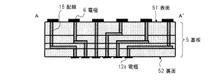
図6は図5に示した線分A−A’の部位の断面図である。図6に示すように、基板5は、表面51に設けられた電極6と、裏面52に設けられた電極12aと、電極6および電極12aを接続する配線15とを有する。電極12aは、図3に示した貫通電極2aと接続される。この構成により、電極6とこの電極6に対応する貫通電極2aとが、電極12aおよび配線15を介して電気的に接続される。電極6が第2の電極に相当し、電極12aが第3の電極に相当する。
FIG. 6 is a cross-sectional view taken along line A-A ′ shown in FIG. 5. As shown in FIG. 6, the
基板5は、絶縁膜を介して複数の配線層が積層された多層配線構造である。図6に示す構成では、電極6が形成される層を含めて配線層が4層の場合を示しているが、配線層は4層の場合に限らない。電極6の数およびレイアウトに応じて、必要な配線層を適宜変更することが可能である。多層配線構造は、例えば、配線層が絶縁膜中の1層と絶縁膜の上の1層とからなる2層構造であってもよい。
The
図7は、図1に示した基板5の裏面における、電極のレイアウトの一例を示す平面図である。図7に示すように、基板5の裏面52には、図3に示した貫通電極2aに対応して、貫通電極2aと同様なピッチおよび配置で電極12aが設けられている。図7に示す構成例では、基板5の裏面52には、配線15を介して電極6と接続される電極12aのみが設けられているが、電極6に接続されない電極が設けられていてもよい。
FIG. 7 is a plan view showing an example of the electrode layout on the back surface of the
図8は、基板5の裏面における、電極のレイアウトの他の例を示す平面図である。図8に示すように、図3に示した貫通電極2の全てに対応して電極12が設けられていてもよい。貫通電極2と同様なピッチおよび配置で電極12が設けられている。ただし、電極12のうち、電極12a以外の電極には配線15が接続されていない。そのため、貫通電極2aと接触する電極12aのみが電極6と電気的に接続される。
FIG. 8 is a plan view showing another example of the electrode layout on the back surface of the
基板5の材料としては、半導体チップ3の貫通電極2aと電気的に接続可能な電極を有する基板であればどのようなものでもよい。例えば、半導体チップ3がシリコンを基板にした半導体デバイスである場合、基板5のベースとして、熱膨張率が半導体チップ3に近いシリコン基板を用いるとよい。
As a material of the
上述した構成により、複数の電極6のそれぞれが、配線15および電極12aを介して複数の貫通電極2aのそれぞれと電気的に接続される。そのため、電極6を介して半導体チップ3と外部との間で信号を入出力することが可能となる。例えば、電極6と電気的に接続される貫通電極2aを、半導体チップ3のテスト信号を伝送するための貫通配線として利用することで、チップ積層体13をパッケージ基板4に実装する前の状態で、電極6を介して半導体チップ3をテストすることが可能となる。チップ積層体13をパッケージ基板4に実装する前に、半導体チップ3をテストする方法については、後で詳しく説明する。
With the configuration described above, each of the plurality of electrodes 6 is electrically connected to each of the plurality of through
次に、チップ積層体13をパッケージ基板4に実装する前の状態で半導体チップ3をテストする方法を説明する前に、チップ積層体13をパッケージ基板4に実装した後の半導体装置1における、半導体チップ3のテストに関連する構成を説明する。
Next, before describing a method for testing the
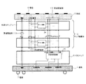
図9は、図1に示した半導体装置において、半導体チップをテストする方法を説明するための断面模式図である。なお、本発明に関連する構成について詳細に説明し、半導体装置1の通常動作に関連する構成を図に示すことと、その詳細な説明を省略する。 FIG. 9 is a schematic cross-sectional view for explaining a method of testing a semiconductor chip in the semiconductor device shown in FIG. The configuration related to the present invention will be described in detail, the configuration related to the normal operation of the semiconductor device 1 is shown in the drawing, and the detailed description thereof is omitted.
図9に示すように、複数の半導体チップ3のそれぞれには、半導体チップ3の動作をテストするための内部回路となるテスト回路24が設けられている。また、ASICチップ8には、複数の半導体チップ3を制御するための内部制御回路18が設けられている。内部制御回路18は、半導体装置1の通常動作時に各半導体チップ3に対してデータの入出力の制御を行い、テスト時に各半導体チップ3のテスト回路24の制御を行う。
As shown in FIG. 9, each of the plurality of
図1から図4を参照して説明した貫通電極2aは、隣り合う半導体チップ3を介して基板5に接続される貫通電極と、隣り合う半導体チップ3およびASICチップ8を介して基板5およびパッケージ基板4の両方に接続される貫通電極とに分類される。基板5に接続される貫通電極のグループを貫通電極群111とし、基板5およびパッケージ基板4の両方に接続される貫通電極のグループを貫通電極群113とする。そして、貫通電極2のうち、貫通電極2aを除いた貫通電極のグループを貫通電極群112とする。貫通電極群112は、隣り合う半導体チップ3およびASICチップ8を介してパッケージ基板4と接続されているが、基板5と接続されている必要はない。
The through
貫通電極群111に属する貫通電極は、隣り合う半導体チップ3を介して基板5に接続され、図9に示していないが、図6に示した配線15を介して電極6に接続されている。貫通電極群111に属する貫通電極は各半導体チップ3のテスト回路28に接続されている。貫通電極群111は、半導体チップ3のテスト信号の伝送線路として機能するが、チップ積層体13をパッケージ基板4に実装した後には使用されない。
The through electrode belonging to the through electrode group 111 is connected to the
貫通電極群112に属する貫通電極は、隣り合う半導体チップ3を介してASICチップ8に接続され、ASICチップ8の内部制御回路18を介してパッケージ基板4の電極7に接続されている。貫通電極群112は、チップ積層体13をパッケージ基板4に実装した後の半導体装置1における半導体チップ3に対して、通常動作時とテスト時のいずれの場合にも、半導体チップ3とASICチップ8との間で信号を伝送するための伝送線路として機能する。伝送される信号の種類として、半導体チップ3がDRAMの場合、例えば、アドレス信号ADD、コマンド信号CMD、およびデータDQ等がある。
The through electrode belonging to the through electrode group 112 is connected to the
貫通電極群113に属する貫通電極は、隣り合う半導体チップ3を介して基板5に接続され、図9に示していないが、図6に示した配線15を介して電極6に接続されている。また、貫通電極群113に属する貫通電極は、隣り合う半導体チップ3を介してASICチップ8に接続され、図9に示していないが、図1に示した貫通電極29を介してパッケージ基板4の電極7に接続されている。
The through electrode belonging to the through electrode group 113 is connected to the
貫通電極群113に属する貫通電極は、各半導体チップ3およびASICチップ8に電源電圧VDDおよび接地電位VSSを供給するための配線として使用される。ここでは、貫通電極群113が、電源電圧VDDおよび接地電位VSSを各チップに供給するための配線として使用される場合で説明するが、外部から入力され、半導体チップ3およびASICチップ8に共通に使用される信号を各チップに伝送するための伝送線路として貫通電極群113を使用してもよい。貫通電極群113は、ASICチップ18を介してパッケージ基板4と接続されている点が貫通電極群112と共通しているが、内部制御回路18等の内部回路を介さずに、パッケージ基板4の電極7と接続されている点が貫通電極群112と異なっている。
The through electrodes belonging to the through electrode group 113 are used as wirings for supplying the power supply voltage VDD and the ground potential VSS to each
ここで、上述した半導体装置1において、通常動作とテストのそれぞれの場合における動作を簡単に説明する。はじめに、半導体装置1における半導体チップ3を通常動作させる場合を説明する。
Here, in the semiconductor device 1 described above, the operation in each of the normal operation and the test will be briefly described. First, the case where the
電源電圧VDDおよび接地電位VSSがパッケージ基板4の電極7および貫通電極群113を介して外部から各チップに供給され、複数の外部信号A〜Zが電極7を介してASICチップ8に入力される。外部信号A〜Zには、複数の半導体チップ3のうち、いずれか1つを指定するためのチップセレクト信号も含まれている。外部信号A〜Zが内部制御回路18で処理された後、ASICチップ8からアドレス信号ADDおよびコマンド信号CMD等の信号が貫通電極群112を介して半導体チップ3に伝送される。データ書き込みの場合には、これらの信号の中にデータDQが含まれている。チップセレクト信号で指定された半導体チップ3は、アドレス信号ADDで特定されるメモリ素子に対して、コマンド信号CMDにしたがって、データDQの読み出し、またはデータDQの書き込みを行う。
The power supply voltage VDD and the ground potential VSS are supplied to each chip from the outside via the electrode 7 and the through electrode group 113 of the package substrate 4, and a plurality of external signals A to Z are input to the
次に、半導体装置1における半導体チップ3のテスト方法を説明する。半導体チップ3のテスト方法として、(1)「基板5の電極6に外部から電源と信号を供給する場合」と、(2)「パッケージ基板4の電極7に外部から電源と信号を供給する場合」の2通りが可能であるが、ここでは(2)の場合を説明し、(1)の場合は後述する。
Next, a method for testing the
電源電圧VDDおよび接地電位VSSがパッケージ基板4の電極7および貫通電極群113を介して外部から各チップに供給され、複数の外部信号A〜Zが電極7を介してASICチップ8に入力される。外部信号A〜Zが内部制御回路18で処理された後、ASICチップ8からアドレス信号ADDおよびコマンド信号CMD等の信号が貫通電極群112を介して半導体チップ3に伝送される。ここでは、アドレス信号ADDおよびコマンド信号CMD等の信号がテスト信号に相当する。チップセレクト信号で指定された半導体チップ3は、ASICチップ8から入力されるテスト信号をテスト回路24に入力し、その結果を貫通電極群112およびASICチップ8を介してパッケージ基板4の電極7に出力する。
The power supply voltage VDD and the ground potential VSS are supplied to each chip from the outside via the electrode 7 and the through electrode group 113 of the package substrate 4, and a plurality of external signals A to Z are input to the
このようにして、パッケージ基板4の電極7および貫通電極群113を介して電源を半導体チップ3に供給し、電極7および貫通電極群112を介してテスト信号を半導体チップ3に伝送することで、半導体チップ3に対するテストの結果を貫通電極群112および電極7を介して出力させることができる。
In this way, by supplying power to the
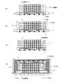
次に、本実施形態の半導体装置の製造方法を説明する。図10(a)〜(d)は本実施形態の半導体装置の製造方法の手順を示す断面図である。ここでは、半導体チップ3、パッケージ基板4、ASICチップ8および基板5のそれぞれの製造方法についての詳細な説明を省略する。また、ASICチップ8を搭載したパッケージ基板4を準備しておくものとする。
Next, a method for manufacturing the semiconductor device of this embodiment will be described. 10A to 10D are cross-sectional views illustrating the procedure of the method for manufacturing the semiconductor device of this embodiment. Here, a detailed description of each method for manufacturing the
図10(a)に示すように、基板5aの上に4つの半導体チップ3を積層してチップ積層体13を作製する。その際、対向する半導体チップ3間で貫通電極2の位置が一致するように、4つの半導体チップ3を積層し、対応する電極同士を接続する。また、最下層の半導体チップ3の貫通電極2aと基板5aの電極12aとを接続させる。基板5aは平面状に複数の基板5が設けられた基板に相当する。温度変化等により貫通電極2の膨張や収縮の際に応力が発生しても、その応力が基板5aで吸収される。
As shown in FIG. 10A, four
図10(b)に示すように、基板5aの上に金型105を配置した後、チップ積層体13の半導体チップ3間の隙間を埋め込み、かつ、半導体チップ3の側面を覆うように、金型105内に樹脂14を流し込む。その際、図10(b)に示すように、金型105内に流し込む樹脂14の上面が最上層の半導体チップ3aの上面を越えないようにする。このようにして、最上層の半導体チップ3aの上面が露出した状態で、半導体チップ3間の隙間、および半導体チップ3と基板5aとの間に、樹脂14が充填される。
As shown in FIG. 10B, after the
続いて、金型105を外した後、基板5aをスクライビングして基板5毎に分離すると、図10(c)に示す構造が得られる。図10(c)に示した構造を用いて、後述のテストを行う。テストの結果、良品と判定された構造に対して、その上下を逆にしてパッケージ基板4のASICチップ8の上に搭載する。ここでは、複数のパッケージ基板4が1枚の基板に設けられている。図10(c)に示した構造をASICチップ8の上に搭載する際、半導体チップ3aの貫通電極2の位置とASICチップ8の貫通電極29の位置が一致するように、チップ積層体13をASICチップ8の上に配置し、対応する電極同士を接続する。
Subsequently, after removing the
その後、図10(d)に示すように、パッケージ基板4の上に金型106を配置し、図10(c)に示した構造の上面および側面を覆うように、金型106内に封止樹脂9を流し込む。その際、封止樹脂9の温度変化等により貫通電極2が膨張または収縮しても、膨張または収縮による応力が最上段に配置された基板5にかかるため、半導体チップ3にクラックが発生するのを防げる。その後、金型106を外した後、パッケージ基板4毎に分離することで、図1に示した半導体装置1が作製される。
Thereafter, as shown in FIG. 10 (d), the
次に、本実施形態の半導体装置1の実装例を説明する。図11は、本実施形態の半導体装置をシステム基板に搭載した場合の断面図である。 Next, a mounting example of the semiconductor device 1 of the present embodiment will be described. FIG. 11 is a cross-sectional view when the semiconductor device of this embodiment is mounted on a system board.
チップ積層体13は、図10(c)に示した構造で後述のテストが行われた後、良品と判定されたものは、図10(d)を参照して説明したように、パッケージ基板4上に実装される。その後、半導体装置1として、図11に示すように、システム基板34に搭載される。図11に示すように、複数の半導体装置1a,1bがシステム基板34に搭載されてもよい。また、図11に示すように、半導体装置1a,1bを制御するコントローラ33がシステム基板34に設けられていてもよい。
As described above with reference to FIG. 10D, the
次に、チップ積層体13をパッケージ基板4に搭載する前に、チップ積層体13を用いて半導体チップ3をテストする方法を説明する。図12はチップ積層体の状態で半導体チップをテストする方法を説明するための断面図である。
Next, a method for testing the
基板5を用いた半導体チップ3のテストは、図10(c)を参照して説明したように、チップ積層体13をパッケージ基板4に搭載する前に行う。図9に示した貫通電極群111に属する貫通電極を半導体チップ3のテスト信号を伝送するための伝送線路として利用する。
The test of the
図に示さない検査装置がケーブルを介して、図12に示すプローブカード104のプローブ針11と接続されている。プローブ針11のピッチは電極6のピッチと同等である。検査装置(不図示)には、チップ積層体13に供給するための電源電圧VDDおよび接地電位VSSと、チップセレクト信号、アドレス信号ADD、コマンド信号CMDおよびデータDQを含むテスト信号とを生成する回路が設けられている。
An inspection apparatus (not shown) is connected to the probe needle 11 of the probe card 104 shown in FIG. 12 via a cable. The pitch of the probe needles 11 is equal to the pitch of the electrodes 6. The inspection device (not shown) generates a power supply voltage VDD and a ground potential VSS to be supplied to the
図12に示すように、チップ積層体13が設けられた基板5をプローブカード104に載せる。その際、基板5の表面51に設けられた電極6とプローブ針11との位置を一致させ、電極6とプローブ針11とを接触させる。続いて、電源電圧VDDおよび接地電位VSSをプローブ針11、基板5の電極6、および図9に示した貫通電極群113を介して検査装置(不図示)から各半導体チップ3に供給する。また、テスト信号をプローブ針11および図9に示した貫通電極群111を介して検査装置から半導体チップ3に伝送する。チップセレクト信号で指定された半導体チップ3は、プローブ針11を介して検査装置から供給されるテスト信号を図9に示したテスト回路24に入力し、その結果を貫通電極群111、基板5の電極6、およびプローブ針11を介して検査装置に送信する。
As shown in FIG. 12, the
このようにして、基板5の電極6および貫通電極群113を介して電源を半導体チップ3に供給し、電極6および貫通電極群111を介してテスト信号を半導体チップ3に伝送することで、半導体チップ3に対するテストの結果が貫通電極群111および電極6を介して出力される。そのため、チップ積層体13をパッケージ基板4に搭載する前に、半導体チップ3の動作を検査することが可能となる。
In this way, the power is supplied to the
また、電極6は、貫通電極2よりも大きいピッチで配列されているため、プローブカード104のプローブ針11のピッチも貫通電極2よりも大きくすることができる。プローブ針11のピッチを大きくすることで、プローブ針11同士の絶縁性を容易に確保することができる。 Further, since the electrodes 6 are arranged with a pitch larger than that of the through electrodes 2, the pitch of the probe needles 11 of the probe card 104 can be made larger than that of the through electrodes 2. By increasing the pitch of the probe needles 11, insulation between the probe needles 11 can be easily ensured.
また、電極6のピッチが既存のプローブカード104のプローブ針11のピッチに合うように基板5を設計し、基板5を作製してもよい。この場合、既に使用されているプローブカード104を、パッケージング前のチップ積層体13のテストに使用することが可能となる。
Further, the
また、チップ積層体13の状態でテストを行うことで、チップ積層体13を作製したとき、隣り合う半導体チップ3間で貫通電極の接続不良があるか否かを判定することが可能となる。このテストで接続不良が見つかったチップ積層体13をその後のパッケージングに使用しないようにすることで、半導体装置1の不良品の発生を抑制できる。
Further, by performing the test in the state of the chip stacked
また、チップ積層体13の状態でテストを行うことで、複数の半導体チップ3を単体の装置として動作させる試験を行うことも可能となる。この段階でチップ積層体13の不具合を見つけられれば、不良と判定されたチップ積層体13を使用しないことで、その後の工程が無駄にならずに済む。
In addition, by performing the test in the state of the
上述したように、チップ積層体13をパッケージングする前に各半導体チップ3が良品であるか否か、貫通電極の接続に不具合があるか否かを判定することができる。テストで良品と判定された半導体チップ3およびチップ積層体13は、基板5を搭載したままパッケージ基板4に実装され、図1に示した半導体装置1が作製される。
As described above, it is possible to determine whether or not each
本実施形態の半導体装置では、複数のチップが積層されたチップ積層体上に、チップの貫通電極と電気的に接続される第2の電極を有する第2の基板が設けられている。そのため、製造プロセスにおける温度変化等により貫通電極の膨張や収縮の際に応力が発生しても、応力を第2の基板に逃がすことで、チップにかかる応力を低減させ、チップにクラックが発生することを防止できる。 In the semiconductor device of the present embodiment, a second substrate having a second electrode that is electrically connected to the through electrode of the chip is provided on a chip stack in which a plurality of chips are stacked. Therefore, even if stress is generated during expansion or contraction of the through electrode due to temperature change in the manufacturing process, the stress applied to the second substrate is reduced, thereby reducing the stress applied to the chip and causing cracks in the chip. Can be prevented.
また、複数の第2の電極が貫通電極のピッチよりも大きい第2のピッチで配列され、かつ、複数の第2の電極が複数の貫通電極のうち、一部の貫通電極とそれぞれ電気的に接続されているため、第2の電極を介してチップと外部との間で信号の入出力を行うことが可能となる。よって、チップ積層体をパッケージ基板に搭載する前の段階で、第2の電極を介して電源およびテスト信号をチップに供給することで、チップ積層体の状態でチップをテストすることができる。 The plurality of second electrodes are arranged at a second pitch larger than the pitch of the through electrodes, and the plurality of second electrodes are electrically connected to some of the through electrodes, respectively. Since they are connected, signal input / output can be performed between the chip and the outside via the second electrode. Therefore, the chip can be tested in the state of the chip stack by supplying the power and the test signal to the chip via the second electrode before the chip stack is mounted on the package substrate.
(第2の実施形態)
第1の実施形態では、種類の同じ複数の半導体チップがパッケージ基板の表面側に実装されていたが、本実施形態は、種類の異なるメモリチップがパッケージ基板の表側に実装された構成である。
(Second Embodiment)
In the first embodiment, a plurality of semiconductor chips of the same type are mounted on the surface side of the package substrate. However, the present embodiment has a configuration in which different types of memory chips are mounted on the front side of the package substrate.
図13は本実施形態の半導体装置の一構成例を示す断面図である。なお、第1の実施形態と同様な構成については同一の符号を付し、その詳細な説明を省略する。 FIG. 13 is a cross-sectional view showing a configuration example of the semiconductor device of this embodiment. In addition, about the structure similar to 1st Embodiment, the same code | symbol is attached | subjected and the detailed description is abbreviate | omitted.
図13に示すように、本実施形態の半導体装置32は、種類の異なるメモリチップ30,31を有する。そして、メモリチップ30,31がパッケージ基板4の表面41側に実装されている。図13に示す構成例では、4つのメモリチップ30が積層され、最上段のメモリチップ30の表面301側に基板5bが設けられている。また、メモリチップ31がパッケージ基板4の上に設けられ、メモリチップ31の表面311側に基板5cが設けられている。以下では、4つのメモリチップ30からなるチップ積層体の上に基板5bが設けられた構成を構造体305と称し、メモリチップ31の上に基板5cが設けられ構成を構造体315と称する。
As shown in FIG. 13, the semiconductor device 32 of the present embodiment includes different types of
基板5bには、貫通電極2のピッチよりも大きいピッチで配列される電極6bが設けられている。基板5cには、貫通電極2のピッチよりも大きいピッチで配列される電極6cが設けられているが、チップ30とチップ31とを接続するための貫通電極35も設けられている。そのため、電極6cは、貫通電極35が形成されていない領域に配置されている。
The substrate 5b is provided with electrodes 6b arranged at a pitch larger than the pitch of the through electrodes 2. The
メモリチップ30,31は、例えば、DRAM、SRAM、PRAM、フラッシュメモリ等の半導体メモリチップである。なお、メモリチップ30の数は4つに限らない。
The
本実施形態の半導体装置32の製造方法は、図10(a)〜(c)を参照して説明した工程およびテストをメモリチップ30,31に対応して行うことを除いて、第1の実施形態と同様になるため、その詳細な説明を省略する。
The manufacturing method of the semiconductor device 32 of the present embodiment is the first implementation except that the processes and tests described with reference to FIGS. 10A to 10C are performed corresponding to the
本実施形態では、構造体305および構造体315のそれぞれについて、パッケージ基板4に実装する前に、第1の実施形態のチップ積層体13に対して行ったテストを行う。具体的に説明すると、構造体305の基板5bに設けられた電極6bを介して電源およびテスト信号をメモリチップ30に供給してメモリチップ30のテストを行う。また、構造体315の基板5cに設けられた電極6cを介して電源およびテスト信号をメモリチップ31に供給してメモリチップ31のテストを行う。
In the present embodiment, each of the structure body 305 and the structure body 315 is tested on the
パッケージ基板4の上に構造体315および構造体305を搭載し、封止樹脂9でこれらの構造体を覆うパッケージング後は、メモリチップ31は電極7を介して外部から電源および信号が供給可能となり、メモリチップ30は電極7、メモリチップ31の貫通電極、基板5cの貫通電極35を介して外部から電源および信号が供給可能となる。
After packaging the structure 315 and the structure 305 on the package substrate 4 and covering these structures with the sealing resin 9, the memory chip 31 can supply power and signals from the outside via the electrodes 7. Thus, the
本実施形態の半導体装置では、メモリチップ30の表面側に基板5bが設けられ、メモリチップ31の表面側に基板5cが設けられているため、製造プロセスでメモリチップ30,31にクラックが発生するのを防止できるだけでなく、パッケージングを行う前に各メモリチップのテストを行うことが可能である。テストで良品となったチップ30およびチップ31をパッケージ基板4上に実装することで、半導体装置32の不良品の発生を抑制できる。
In the semiconductor device of this embodiment, the substrate 5b is provided on the front surface side of the
1、1a、1b、32 半導体装置
2、2a 貫通電極
3、3a 半導体チップ
4 パッケージ基板
5、5a、5b、5c 基板
6、6b、6c、7 電極
30、31 メモリチップ
1, 1a, 1b, 32
Claims (9)
前記複数の第1の電極とそれぞれ電気的に接続され、第1のピッチで配列された複数の貫通電極をそれぞれ有する複数の第1のチップが積層され、前記第1の基板の前記表面側に設けられたチップ積層体と、
前記チップ積層体を基準にして、前記第1の基板とは反対側に設けられた第2の基板とを有し、
前記第2の基板は、前記複数の貫通電極のうち、一部の貫通電極とそれぞれ電気的に接続され、前記第1のピッチよりも大きい第2のピッチで配列された複数の第2の電極を有する、半導体装置。 A first substrate having two surfaces, a front surface and a back surface, and a plurality of first electrodes provided on the back surface;
A plurality of first chips that are electrically connected to the plurality of first electrodes and each have a plurality of through electrodes arranged at a first pitch are stacked on the surface side of the first substrate. A provided chip stack;
A second substrate provided on the opposite side of the first substrate with respect to the chip stack,
The second substrate is a plurality of second electrodes that are electrically connected to some of the plurality of through electrodes and arranged at a second pitch that is larger than the first pitch. A semiconductor device.
前記一部の貫通電極は、前記第1のチップのテスト時に使用される信号を伝送するための伝送線路として機能する、半導体装置。 The semiconductor device according to claim 1,
The partial penetration electrode functions as a transmission line for transmitting a signal used when testing the first chip.
前記第2のピッチは、前記第1のチップのテスト時に使用され、前記複数の第2の電極と接触する複数のプローブ針のピッチと同等である、半導体装置。 The semiconductor device according to claim 2,
The semiconductor device, wherein the second pitch is equal to a pitch of a plurality of probe needles that are used when testing the first chip and are in contact with the plurality of second electrodes.
前記第1のチップは半導体チップであり、
前記チップ積層体と前記第1の基板との間に、複数の前記半導体チップを制御するためのコントローラチップが設けられている、半導体装置。 The semiconductor device according to any one of claims 1 to 3,
The first chip is a semiconductor chip;
A semiconductor device, wherein a controller chip for controlling a plurality of the semiconductor chips is provided between the chip stack and the first substrate.
前記複数の第2の電極は、前記第2の基板に設けられた2つの面のうち、前記チップ積層体に対向する面である裏面とは反対側の面である表面に設けられている、半導体装置。 The semiconductor device according to any one of claims 1 to 4,
The plurality of second electrodes are provided on a surface which is a surface opposite to a back surface which is a surface facing the chip stacked body, of two surfaces provided on the second substrate. Semiconductor device.
前記第2の基板は、
前記表面に設けられた前記複数の第2の電極と、
前記裏面に設けられ、前記第2のピッチと同等なピッチで配列された複数の第3の電極と、
前記複数の第2の電極のそれぞれと前記複数の第3の電極のそれぞれとを接続する複数の配線とを有する、半導体装置。 The semiconductor device according to claim 5.
The second substrate is
The plurality of second electrodes provided on the surface;
A plurality of third electrodes provided on the back surface and arranged at a pitch equivalent to the second pitch;
A semiconductor device having a plurality of wirings connecting each of the plurality of second electrodes and each of the plurality of third electrodes.
前記複数の第2の電極のそれぞれは、平面パターンの面積が前記貫通電極の平面パターンの面積よりも大きい、半導体装置。 The semiconductor device according to claim 1,
Each of the plurality of second electrodes is a semiconductor device in which an area of a planar pattern is larger than an area of the planar pattern of the through electrode.
前記チップ積層体および前記第2の基板を覆う絶縁膜を有し、
前記第1の電極は前記絶縁膜には覆われていない、半導体装置。 The semiconductor device according to claim 1,
An insulating film covering the chip stack and the second substrate;
The semiconductor device, wherein the first electrode is not covered with the insulating film.
前記第1の電極は、前記第1のピッチよりも大きい第3のピッチで配列されている、半導体装置。 The semiconductor device according to any one of claims 1 to 8,
The semiconductor device, wherein the first electrodes are arranged with a third pitch larger than the first pitch.
Priority Applications (2)
| Application Number | Priority Date | Filing Date | Title |
|---|---|---|---|
| JP2011012926A JP2012156238A (en) | 2011-01-25 | 2011-01-25 | Semiconductor device |
| US13/353,874 US20120187401A1 (en) | 2011-01-25 | 2012-01-19 | Device allowing suppression of stress on chip |
Applications Claiming Priority (1)
| Application Number | Priority Date | Filing Date | Title |
|---|---|---|---|
| JP2011012926A JP2012156238A (en) | 2011-01-25 | 2011-01-25 | Semiconductor device |
Publications (1)
| Publication Number | Publication Date |
|---|---|
| JP2012156238A true JP2012156238A (en) | 2012-08-16 |
Family
ID=46543522
Family Applications (1)
| Application Number | Title | Priority Date | Filing Date |
|---|---|---|---|
| JP2011012926A Withdrawn JP2012156238A (en) | 2011-01-25 | 2011-01-25 | Semiconductor device |
Country Status (2)
| Country | Link |
|---|---|
| US (1) | US20120187401A1 (en) |
| JP (1) | JP2012156238A (en) |
Cited By (6)
| Publication number | Priority date | Publication date | Assignee | Title |
|---|---|---|---|---|
| JP2014072289A (en) * | 2012-09-28 | 2014-04-21 | Renesas Electronics Corp | Semiconductor device |
| WO2014061426A1 (en) * | 2012-10-15 | 2014-04-24 | ピーエスフォー ルクスコ エスエイアールエル | Semiconductor device |
| JP2016171124A (en) * | 2015-03-11 | 2016-09-23 | 株式会社東芝 | Semiconductor device and manufacturing method thereof |
| JP2018160490A (en) * | 2017-03-22 | 2018-10-11 | 富士通株式会社 | Electronic device, manufacturing method thereof, and electronic component |
| JP2021197541A (en) * | 2020-06-10 | 2021-12-27 | インテル コーポレイション | High-speed memory system integration |
| JP2024527645A (en) * | 2022-07-08 | 2024-07-26 | チャンシン メモリー テクノロジーズ インコーポレイテッド | Semiconductor package structure and manufacturing method |
Families Citing this family (3)
| Publication number | Priority date | Publication date | Assignee | Title |
|---|---|---|---|---|
| KR101977699B1 (en) * | 2012-08-20 | 2019-08-28 | 에스케이하이닉스 주식회사 | Multi chip semiconductor apparatus and method of testing the same |
| US10057976B1 (en) * | 2017-08-31 | 2018-08-21 | Xilinx, Inc. | Power-ground co-reference transceiver structure to deliver ultra-low crosstalk |
| JP2019054181A (en) * | 2017-09-19 | 2019-04-04 | 東芝メモリ株式会社 | Semiconductor package |
Family Cites Families (8)
| Publication number | Priority date | Publication date | Assignee | Title |
|---|---|---|---|---|
| JP3888302B2 (en) * | 2002-12-24 | 2007-02-28 | カシオ計算機株式会社 | Semiconductor device |
| JP4507101B2 (en) * | 2005-06-30 | 2010-07-21 | エルピーダメモリ株式会社 | Semiconductor memory device and manufacturing method thereof |
| JP5352146B2 (en) * | 2008-07-23 | 2013-11-27 | ルネサスエレクトロニクス株式会社 | Semiconductor device |
| JP2010245383A (en) * | 2009-04-08 | 2010-10-28 | Elpida Memory Inc | Semiconductor device and manufacturing method of semiconductor device |
| JP5543125B2 (en) * | 2009-04-08 | 2014-07-09 | ピーエスフォー ルクスコ エスエイアールエル | Semiconductor device and manufacturing method of semiconductor device |
| EP2302403A1 (en) * | 2009-09-28 | 2011-03-30 | Imec | Method and device for testing TSVs in a 3D chip stack |
| JP5448698B2 (en) * | 2009-10-09 | 2014-03-19 | ピーエスフォー ルクスコ エスエイアールエル | Semiconductor device and test method thereof |
| JP5601842B2 (en) * | 2010-01-18 | 2014-10-08 | ピーエスフォー ルクスコ エスエイアールエル | Semiconductor device, semiconductor device test method, and data processing system |
-
2011
- 2011-01-25 JP JP2011012926A patent/JP2012156238A/en not_active Withdrawn
-
2012
- 2012-01-19 US US13/353,874 patent/US20120187401A1/en not_active Abandoned
Cited By (8)
| Publication number | Priority date | Publication date | Assignee | Title |
|---|---|---|---|---|
| JP2014072289A (en) * | 2012-09-28 | 2014-04-21 | Renesas Electronics Corp | Semiconductor device |
| WO2014061426A1 (en) * | 2012-10-15 | 2014-04-24 | ピーエスフォー ルクスコ エスエイアールエル | Semiconductor device |
| DE112013004993B4 (en) * | 2012-10-15 | 2020-09-10 | Longitude Licensing Ltd. | Semiconductor device |
| JP2016171124A (en) * | 2015-03-11 | 2016-09-23 | 株式会社東芝 | Semiconductor device and manufacturing method thereof |
| JP2018160490A (en) * | 2017-03-22 | 2018-10-11 | 富士通株式会社 | Electronic device, manufacturing method thereof, and electronic component |
| JP2021197541A (en) * | 2020-06-10 | 2021-12-27 | インテル コーポレイション | High-speed memory system integration |
| JP2024527645A (en) * | 2022-07-08 | 2024-07-26 | チャンシン メモリー テクノロジーズ インコーポレイテッド | Semiconductor package structure and manufacturing method |
| JP7650293B2 (en) | 2022-07-08 | 2025-03-24 | チャンシン メモリー テクノロジーズ インコーポレイテッド | Semiconductor package structure and manufacturing method |
Also Published As
| Publication number | Publication date |
|---|---|
| US20120187401A1 (en) | 2012-07-26 |
Similar Documents
| Publication | Publication Date | Title |
|---|---|---|
| JP2012156238A (en) | Semiconductor device | |
| US9329227B2 (en) | Method and apparatus for testing interconnection reliability of a ball grid array on a testing printed circuit board | |
| US7675181B2 (en) | Planar multi semiconductor chip package and method of manufacturing the same | |
| JP6054029B2 (en) | Semiconductor chip and semiconductor device | |
| JP5932324B2 (en) | Semiconductor device and test method thereof | |
| KR20130044048A (en) | Semiconductor wafer and method for fabricating stack package using the same | |
| KR20120035297A (en) | Semiconductor package and method of manufacturing the semiconductor package | |
| US9947457B2 (en) | Pre space transformer, space transformer manufactured using the pre space transformer, and semiconductor device inspecting apparatus including the space transformer | |
| WO2014077154A1 (en) | Semiconductor device | |
| JP2008085342A (en) | Method for identifying and / or programming an integrated circuit | |
| JP4343256B1 (en) | Manufacturing method of semiconductor device | |
| KR101431915B1 (en) | Pre space transformer and space transformer manufactured by the pre space transformer, and apparatus for inspecting semiconductor device with the space transformer | |
| US9659887B2 (en) | Semiconductor device | |
| JP2011139040A (en) | Semiconductor device, probe test method and manufacturing method of the same | |
| CN106206338A (en) | Printed circuit board (PCB) and method of testing thereof and the method manufacturing semiconductor packages | |
| US8717059B2 (en) | Die having wire bond alignment sensing structures | |
| WO2011115041A1 (en) | Semiconductor device manufacturing method and semiconductor device | |
| JP2006351588A (en) | Semiconductor device and manufacturing method thereof | |
| JP2012156327A (en) | Semiconductor device and laminate semiconductor device | |
| US20120193622A1 (en) | Device | |
| JP5123559B2 (en) | Semiconductor device and manufacturing method thereof | |
| JP5407925B2 (en) | Integrated circuit device manufacturing method and inspection device | |
| JP2008130905A (en) | Semiconductor device manufacturing method and test apparatus therefor | |
| CN113437041A (en) | Semiconductor substrate, semiconductor package including the same, and test method thereof | |
| US7154116B2 (en) | Rewiring substrate strip with a number of semiconductor component positions |
Legal Events
| Date | Code | Title | Description |
|---|---|---|---|
| A711 | Notification of change in applicant |
Free format text: JAPANESE INTERMEDIATE CODE: A711 Effective date: 20130730 |
|
| A621 | Written request for application examination |
Free format text: JAPANESE INTERMEDIATE CODE: A621 Effective date: 20140122 |
|
| RD04 | Notification of resignation of power of attorney |
Free format text: JAPANESE INTERMEDIATE CODE: A7424 Effective date: 20140411 |
|
| A761 | Written withdrawal of application |
Free format text: JAPANESE INTERMEDIATE CODE: A761 Effective date: 20141009 |