JP2012156286A - 赤外線センサ - Google Patents
赤外線センサ Download PDFInfo
- Publication number
- JP2012156286A JP2012156286A JP2011013666A JP2011013666A JP2012156286A JP 2012156286 A JP2012156286 A JP 2012156286A JP 2011013666 A JP2011013666 A JP 2011013666A JP 2011013666 A JP2011013666 A JP 2011013666A JP 2012156286 A JP2012156286 A JP 2012156286A
- Authority
- JP
- Japan
- Prior art keywords
- metal layer
- semiconductor substrate
- infrared sensor
- mim diode
- lower metal
- Prior art date
- Legal status (The legal status is an assumption and is not a legal conclusion. Google has not performed a legal analysis and makes no representation as to the accuracy of the status listed.)
- Granted
Links
- 229910052751 metal Inorganic materials 0.000 claims abstract description 62
- 239000002184 metal Substances 0.000 claims abstract description 62
- 239000004065 semiconductor Substances 0.000 claims abstract description 44
- 239000000758 substrate Substances 0.000 claims abstract description 41
- 230000003287 optical effect Effects 0.000 claims description 4
- 239000011347 resin Substances 0.000 claims description 4
- 229920005989 resin Polymers 0.000 claims description 4
- 230000001590 oxidative effect Effects 0.000 claims description 3
- 229910052782 aluminium Inorganic materials 0.000 claims 1
- WABPQHHGFIMREM-UHFFFAOYSA-N lead(0) Chemical compound [Pb] WABPQHHGFIMREM-UHFFFAOYSA-N 0.000 claims 1
- 150000002739 metals Chemical class 0.000 claims 1
- 229910052759 nickel Inorganic materials 0.000 claims 1
- 229910052697 platinum Inorganic materials 0.000 claims 1
- 229910052719 titanium Inorganic materials 0.000 claims 1
- 230000035945 sensitivity Effects 0.000 abstract description 7
- 239000011248 coating agent Substances 0.000 abstract description 3
- 238000000576 coating method Methods 0.000 abstract description 3
- 238000009413 insulation Methods 0.000 abstract description 3
- 238000003475 lamination Methods 0.000 abstract 1
- 239000010410 layer Substances 0.000 description 84
- 238000001514 detection method Methods 0.000 description 10
- 238000000609 electron-beam lithography Methods 0.000 description 8
- 238000004519 manufacturing process Methods 0.000 description 7
- 238000012545 processing Methods 0.000 description 7
- 230000000694 effects Effects 0.000 description 6
- XUIMIQQOPSSXEZ-UHFFFAOYSA-N Silicon Chemical compound [Si] XUIMIQQOPSSXEZ-UHFFFAOYSA-N 0.000 description 5
- 230000004888 barrier function Effects 0.000 description 5
- 238000000034 method Methods 0.000 description 5
- 230000004044 response Effects 0.000 description 5
- 229910052710 silicon Inorganic materials 0.000 description 5
- 239000010703 silicon Substances 0.000 description 5
- 239000011247 coating layer Substances 0.000 description 4
- 229910018507 Al—Ni Inorganic materials 0.000 description 3
- 229910018525 Al—Pt Inorganic materials 0.000 description 3
- 229910018575 Al—Ti Inorganic materials 0.000 description 3
- 239000000463 material Substances 0.000 description 3
- 230000008569 process Effects 0.000 description 3
- 229910018173 Al—Al Inorganic materials 0.000 description 2
- CURLTUGMZLYLDI-UHFFFAOYSA-N Carbon dioxide Chemical compound O=C=O CURLTUGMZLYLDI-UHFFFAOYSA-N 0.000 description 2
- VYPSYNLAJGMNEJ-UHFFFAOYSA-N Silicium dioxide Chemical compound O=[Si]=O VYPSYNLAJGMNEJ-UHFFFAOYSA-N 0.000 description 2
- 239000004020 conductor Substances 0.000 description 2
- 238000001816 cooling Methods 0.000 description 2
- 230000007423 decrease Effects 0.000 description 2
- 238000000151 deposition Methods 0.000 description 2
- 229910052814 silicon oxide Inorganic materials 0.000 description 2
- 238000004378 air conditioning Methods 0.000 description 1
- QVGXLLKOCUKJST-UHFFFAOYSA-N atomic oxygen Chemical compound [O] QVGXLLKOCUKJST-UHFFFAOYSA-N 0.000 description 1
- 230000008901 benefit Effects 0.000 description 1
- 230000015572 biosynthetic process Effects 0.000 description 1
- 229910002092 carbon dioxide Inorganic materials 0.000 description 1
- 239000001569 carbon dioxide Substances 0.000 description 1
- 239000000919 ceramic Substances 0.000 description 1
- 230000008859 change Effects 0.000 description 1
- 238000011109 contamination Methods 0.000 description 1
- 238000010411 cooking Methods 0.000 description 1
- 238000011161 development Methods 0.000 description 1
- 230000005684 electric field Effects 0.000 description 1
- 230000005674 electromagnetic induction Effects 0.000 description 1
- 238000005530 etching Methods 0.000 description 1
- 238000007654 immersion Methods 0.000 description 1
- 150000002500 ions Chemical class 0.000 description 1
- 238000010030 laminating Methods 0.000 description 1
- 238000005259 measurement Methods 0.000 description 1
- 239000007769 metal material Substances 0.000 description 1
- 238000012544 monitoring process Methods 0.000 description 1
- 229910052760 oxygen Inorganic materials 0.000 description 1
- 239000001301 oxygen Substances 0.000 description 1
- 238000004806 packaging method and process Methods 0.000 description 1
- 238000000059 patterning Methods 0.000 description 1
- 230000000149 penetrating effect Effects 0.000 description 1
Images

Landscapes
- Light Receiving Elements (AREA)
- Photometry And Measurement Of Optical Pulse Characteristics (AREA)
Abstract
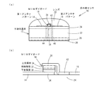
【解決手段】検知対象の波長に対応した長さで、半導体基板12上に形成された一対のアンテナパターン14,16を有する。下金属層30、絶縁層32及び上金属層34の3層から成り、一対のアンテナパターン14,16の間に設けられ、アンテナパターン14,16により検出された電磁波を整流するMIMダイオード18を備える。MIMダイオード18は、下金属層30、絶縁層32、及び上金属層34が厚み向に積層して設けられ、下金属層30及び上金属層34が一対のアンテナパターン14,16の互いに対向する端部にそれぞれ接続している。アンテナパターン14,16及びMIMダイオード18は、半導体基板12上に設けられた集光レンズ20により覆われている。レンズ20は、アンテナパターン14,16を被覆して半導体基板12上に一体に設けられている。
【選択図】図2
Description
12 半導体基板
14 第1アンテナパターン
16 第2アンテナパターン
18 MIMダイオード
20 レンズ
30 下金属層
32 絶縁層
34 上金属層
Claims (6)
- 検知対象の電磁波である赤外線の波長に対応した長さで半導体基板上に形成された一対のアンテナパターンと、下金属層、絶縁層及び上金属層の3層から成り前記一対のアンテナパターンの間に設けられ、このアンテナパターンにより検出された電磁波を整流するMIMダイオードとを備え、
前記MIMダイオードは、前記3層が厚み向に積層して設けられ、前記下金属層及び前記上金属層が前記一対のアンテナパターンの互いに対向する端部にそれぞれ接続されていることを特徴とする赤外線センサ。 - 前記MIMダイオードの下金属層と上金属層は、Al、Pt、Ti、Niの中から選ばれた同一又は異種の金属から成る請求項1記載の赤外線センサ。
- 前記MIMダイオードの下金属層は、前記アンテナパターンと連続して形成されたAlであり、前記下金属層の表面を酸化して、前記絶縁層が形成されている請求項2記載の赤外線センサ。
- 前記アンテナパターン及びMIMダイオードは、前記半導体基板上に設けられた集光レンズにより覆われている請求項1,2又は3記載の赤外線センサ。
- 前記集光レンズは光学用の樹脂から成り、前記アンテナパターンを被覆して前記半導体基板上に一体に設けられている請求項4記載の赤外線センサ。
- 前記MIMダイオードに接続した前記アンテナパターンの端部から前記MIMダイオード近傍で延びた引出線が、前記半導体基板に設けられたビアを介して前記半導体基板裏面に引き出されている請求項1,2又は3記載の赤外線センサ。
Priority Applications (1)
| Application Number | Priority Date | Filing Date | Title |
|---|---|---|---|
| JP2011013666A JP5442648B2 (ja) | 2011-01-26 | 2011-01-26 | 赤外線センサ |
Applications Claiming Priority (1)
| Application Number | Priority Date | Filing Date | Title |
|---|---|---|---|
| JP2011013666A JP5442648B2 (ja) | 2011-01-26 | 2011-01-26 | 赤外線センサ |
Publications (2)
| Publication Number | Publication Date |
|---|---|
| JP2012156286A true JP2012156286A (ja) | 2012-08-16 |
| JP5442648B2 JP5442648B2 (ja) | 2014-03-12 |
Family
ID=46837715
Family Applications (1)
| Application Number | Title | Priority Date | Filing Date |
|---|---|---|---|
| JP2011013666A Expired - Fee Related JP5442648B2 (ja) | 2011-01-26 | 2011-01-26 | 赤外線センサ |
Country Status (1)
| Country | Link |
|---|---|
| JP (1) | JP5442648B2 (ja) |
Cited By (3)
| Publication number | Priority date | Publication date | Assignee | Title |
|---|---|---|---|---|
| JP2015164147A (ja) * | 2014-02-28 | 2015-09-10 | 国立研究開発法人情報通信研究機構 | 光検出器、電気光学装置および光検出器の製造方法 |
| WO2020145233A1 (ja) * | 2019-01-08 | 2020-07-16 | パイオニア株式会社 | 電磁波検出装置及び電磁波検出システム |
| CN115290953A (zh) * | 2022-06-24 | 2022-11-04 | 杭州格蓝丰纳米科技有限公司 | 一种基于动态二极管的自驱动机械信号传感器及其制备方法 |
Citations (6)
| Publication number | Priority date | Publication date | Assignee | Title |
|---|---|---|---|---|
| JPS62222678A (ja) * | 1986-03-25 | 1987-09-30 | Toshiba Corp | 検波器 |
| JPH05264343A (ja) * | 1992-03-19 | 1993-10-12 | Advance Co Ltd | 遠赤外線分光検出素子 |
| JPH06151973A (ja) * | 1992-11-10 | 1994-05-31 | Sharp Corp | 光半導体装置 |
| JP2001296183A (ja) * | 2000-04-17 | 2001-10-26 | Toyota Motor Corp | 赤外線検出装置並びに赤外線画像処理装置 |
| JP2001320629A (ja) * | 1992-04-20 | 2001-11-16 | Loral Vought Systems Corp | 非冷却赤外線検出装置 |
| WO2007129547A1 (ja) * | 2006-05-10 | 2007-11-15 | Murata Manufacturing Co., Ltd. | 赤外線センサおよびその製造方法 |
-
2011
- 2011-01-26 JP JP2011013666A patent/JP5442648B2/ja not_active Expired - Fee Related
Patent Citations (6)
| Publication number | Priority date | Publication date | Assignee | Title |
|---|---|---|---|---|
| JPS62222678A (ja) * | 1986-03-25 | 1987-09-30 | Toshiba Corp | 検波器 |
| JPH05264343A (ja) * | 1992-03-19 | 1993-10-12 | Advance Co Ltd | 遠赤外線分光検出素子 |
| JP2001320629A (ja) * | 1992-04-20 | 2001-11-16 | Loral Vought Systems Corp | 非冷却赤外線検出装置 |
| JPH06151973A (ja) * | 1992-11-10 | 1994-05-31 | Sharp Corp | 光半導体装置 |
| JP2001296183A (ja) * | 2000-04-17 | 2001-10-26 | Toyota Motor Corp | 赤外線検出装置並びに赤外線画像処理装置 |
| WO2007129547A1 (ja) * | 2006-05-10 | 2007-11-15 | Murata Manufacturing Co., Ltd. | 赤外線センサおよびその製造方法 |
Cited By (4)
| Publication number | Priority date | Publication date | Assignee | Title |
|---|---|---|---|---|
| JP2015164147A (ja) * | 2014-02-28 | 2015-09-10 | 国立研究開発法人情報通信研究機構 | 光検出器、電気光学装置および光検出器の製造方法 |
| WO2020145233A1 (ja) * | 2019-01-08 | 2020-07-16 | パイオニア株式会社 | 電磁波検出装置及び電磁波検出システム |
| CN115290953A (zh) * | 2022-06-24 | 2022-11-04 | 杭州格蓝丰纳米科技有限公司 | 一种基于动态二极管的自驱动机械信号传感器及其制备方法 |
| CN115290953B (zh) * | 2022-06-24 | 2024-05-17 | 杭州格蓝丰科技有限公司 | 一种基于动态二极管的自驱动机械信号传感器及其制备方法 |
Also Published As
| Publication number | Publication date |
|---|---|
| JP5442648B2 (ja) | 2014-03-12 |
Similar Documents
| Publication | Publication Date | Title |
|---|---|---|
| US8304850B2 (en) | Integrated infrared sensors with optical elements, and methods | |
| JP5937006B2 (ja) | 単一またはいくつかの層のグラフェン・ベースの光検出デバイスおよびその形成方法 | |
| US9240539B2 (en) | Efficient polarization independent single photon detector | |
| US8975645B2 (en) | Optical filter | |
| US8598528B2 (en) | Infrared detector based on suspended bolometric micro-plates | |
| CN102272563B (zh) | 光检测器 | |
| KR101683257B1 (ko) | 광 검출기 | |
| JP2012002603A (ja) | ボロメータ型テラヘルツ波検出器 | |
| WO2005008787A1 (ja) | 光検出素子 | |
| US20170241836A1 (en) | Apparatus for spectrometrically capturing light with a photodiode which is monolithically integrated in the layer structure of a wavelength-selective filter | |
| JP2018041965A (ja) | 受発光素子およびこれを用いたセンサ装置 | |
| EP2638574A1 (en) | Plasmon induced hot carrier device, method for using the same, and method for manufacturing the same | |
| JP5442648B2 (ja) | 赤外線センサ | |
| KR102349955B1 (ko) | 다중 검출 모드를 지닌 포토 센서 및 그 동작 방법 | |
| JP2007171174A (ja) | 熱型赤外線検出装置およびその製造方法 | |
| JP5531275B2 (ja) | 赤外線センサ及びその製造方法 | |
| KR101942094B1 (ko) | 산소 리치 바나듐산화물 전자파 센서 및 그 시스템 | |
| JP2019090739A (ja) | 熱型赤外線検出器およびその製造方法 | |
| JP2019075562A (ja) | ヘルムホルツ共振器を備える光検出器 | |
| JPH05264343A (ja) | 遠赤外線分光検出素子 | |
| CN113363335A (zh) | 一种红外传感器 | |
| CN111373230A (zh) | 红外装置 | |
| KR101047363B1 (ko) | 자가 발전이 가능한 다중 기능 센서 및 이의 제조 방법 | |
| KR102203338B1 (ko) | 그래파이트 기반의 광 검출기 및 그 제조 방법 | |
| US20250237552A1 (en) | Frequency modulation based ir with doped pcm layer and related methods |
Legal Events
| Date | Code | Title | Description |
|---|---|---|---|
| A621 | Written request for application examination |
Free format text: JAPANESE INTERMEDIATE CODE: A621 Effective date: 20120511 |
|
| A131 | Notification of reasons for refusal |
Free format text: JAPANESE INTERMEDIATE CODE: A131 Effective date: 20130723 |
|
| A977 | Report on retrieval |
Free format text: JAPANESE INTERMEDIATE CODE: A971007 Effective date: 20130724 |
|
| A521 | Request for written amendment filed |
Free format text: JAPANESE INTERMEDIATE CODE: A523 Effective date: 20130924 |
|
| TRDD | Decision of grant or rejection written | ||
| A01 | Written decision to grant a patent or to grant a registration (utility model) |
Free format text: JAPANESE INTERMEDIATE CODE: A01 Effective date: 20131203 |
|
| A61 | First payment of annual fees (during grant procedure) |
Free format text: JAPANESE INTERMEDIATE CODE: A61 Effective date: 20131218 |
|
| R150 | Certificate of patent or registration of utility model |
Free format text: JAPANESE INTERMEDIATE CODE: R150 |
|
| LAPS | Cancellation because of no payment of annual fees |