JP2012164894A - 液体噴射ヘッド及び液体噴射装置並びに圧電素子 - Google Patents
液体噴射ヘッド及び液体噴射装置並びに圧電素子 Download PDFInfo
- Publication number
- JP2012164894A JP2012164894A JP2011025460A JP2011025460A JP2012164894A JP 2012164894 A JP2012164894 A JP 2012164894A JP 2011025460 A JP2011025460 A JP 2011025460A JP 2011025460 A JP2011025460 A JP 2011025460A JP 2012164894 A JP2012164894 A JP 2012164894A
- Authority
- JP
- Japan
- Prior art keywords
- piezoelectric layer
- electrode
- piezoelectric
- layer
- film
- Prior art date
- Legal status (The legal status is an assumption and is not a legal conclusion. Google has not performed a legal analysis and makes no representation as to the accuracy of the status listed.)
- Granted
Links
Images





Classifications
-
- B—PERFORMING OPERATIONS; TRANSPORTING
- B41—PRINTING; LINING MACHINES; TYPEWRITERS; STAMPS
- B41J—TYPEWRITERS; SELECTIVE PRINTING MECHANISMS, i.e. MECHANISMS PRINTING OTHERWISE THAN FROM A FORME; CORRECTION OF TYPOGRAPHICAL ERRORS
- B41J2/00—Typewriters or selective printing mechanisms characterised by the printing or marking process for which they are designed
- B41J2/005—Typewriters or selective printing mechanisms characterised by the printing or marking process for which they are designed characterised by bringing liquid or particles selectively into contact with a printing material
- B41J2/01—Ink jet
- B41J2/135—Nozzles
- B41J2/16—Production of nozzles
- B41J2/1607—Production of print heads with piezoelectric elements
- B41J2/161—Production of print heads with piezoelectric elements of film type, deformed by bending and disposed on a diaphragm
-
- B—PERFORMING OPERATIONS; TRANSPORTING
- B41—PRINTING; LINING MACHINES; TYPEWRITERS; STAMPS
- B41J—TYPEWRITERS; SELECTIVE PRINTING MECHANISMS, i.e. MECHANISMS PRINTING OTHERWISE THAN FROM A FORME; CORRECTION OF TYPOGRAPHICAL ERRORS
- B41J2/00—Typewriters or selective printing mechanisms characterised by the printing or marking process for which they are designed
- B41J2/005—Typewriters or selective printing mechanisms characterised by the printing or marking process for which they are designed characterised by bringing liquid or particles selectively into contact with a printing material
- B41J2/01—Ink jet
- B41J2/135—Nozzles
- B41J2/14—Structure thereof only for on-demand ink jet heads
- B41J2/14201—Structure of print heads with piezoelectric elements
- B41J2/14233—Structure of print heads with piezoelectric elements of film type, deformed by bending and disposed on a diaphragm
-
- B—PERFORMING OPERATIONS; TRANSPORTING
- B41—PRINTING; LINING MACHINES; TYPEWRITERS; STAMPS
- B41J—TYPEWRITERS; SELECTIVE PRINTING MECHANISMS, i.e. MECHANISMS PRINTING OTHERWISE THAN FROM A FORME; CORRECTION OF TYPOGRAPHICAL ERRORS
- B41J2/00—Typewriters or selective printing mechanisms characterised by the printing or marking process for which they are designed
- B41J2/005—Typewriters or selective printing mechanisms characterised by the printing or marking process for which they are designed characterised by bringing liquid or particles selectively into contact with a printing material
- B41J2/01—Ink jet
- B41J2/135—Nozzles
- B41J2/16—Production of nozzles
- B41J2/1621—Manufacturing processes
- B41J2/1623—Manufacturing processes bonding and adhesion
-
- B—PERFORMING OPERATIONS; TRANSPORTING
- B41—PRINTING; LINING MACHINES; TYPEWRITERS; STAMPS
- B41J—TYPEWRITERS; SELECTIVE PRINTING MECHANISMS, i.e. MECHANISMS PRINTING OTHERWISE THAN FROM A FORME; CORRECTION OF TYPOGRAPHICAL ERRORS
- B41J2/00—Typewriters or selective printing mechanisms characterised by the printing or marking process for which they are designed
- B41J2/005—Typewriters or selective printing mechanisms characterised by the printing or marking process for which they are designed characterised by bringing liquid or particles selectively into contact with a printing material
- B41J2/01—Ink jet
- B41J2/135—Nozzles
- B41J2/16—Production of nozzles
- B41J2/1621—Manufacturing processes
- B41J2/1626—Manufacturing processes etching
- B41J2/1629—Manufacturing processes etching wet etching
-
- B—PERFORMING OPERATIONS; TRANSPORTING
- B41—PRINTING; LINING MACHINES; TYPEWRITERS; STAMPS
- B41J—TYPEWRITERS; SELECTIVE PRINTING MECHANISMS, i.e. MECHANISMS PRINTING OTHERWISE THAN FROM A FORME; CORRECTION OF TYPOGRAPHICAL ERRORS
- B41J2/00—Typewriters or selective printing mechanisms characterised by the printing or marking process for which they are designed
- B41J2/005—Typewriters or selective printing mechanisms characterised by the printing or marking process for which they are designed characterised by bringing liquid or particles selectively into contact with a printing material
- B41J2/01—Ink jet
- B41J2/135—Nozzles
- B41J2/16—Production of nozzles
- B41J2/1621—Manufacturing processes
- B41J2/1635—Manufacturing processes dividing the wafer into individual chips
-
- B—PERFORMING OPERATIONS; TRANSPORTING
- B41—PRINTING; LINING MACHINES; TYPEWRITERS; STAMPS
- B41J—TYPEWRITERS; SELECTIVE PRINTING MECHANISMS, i.e. MECHANISMS PRINTING OTHERWISE THAN FROM A FORME; CORRECTION OF TYPOGRAPHICAL ERRORS
- B41J2/00—Typewriters or selective printing mechanisms characterised by the printing or marking process for which they are designed
- B41J2/005—Typewriters or selective printing mechanisms characterised by the printing or marking process for which they are designed characterised by bringing liquid or particles selectively into contact with a printing material
- B41J2/01—Ink jet
- B41J2/135—Nozzles
- B41J2/16—Production of nozzles
- B41J2/1621—Manufacturing processes
- B41J2/164—Manufacturing processes thin film formation
- B41J2/1642—Manufacturing processes thin film formation thin film formation by CVD [chemical vapor deposition]
-
- B—PERFORMING OPERATIONS; TRANSPORTING
- B41—PRINTING; LINING MACHINES; TYPEWRITERS; STAMPS
- B41J—TYPEWRITERS; SELECTIVE PRINTING MECHANISMS, i.e. MECHANISMS PRINTING OTHERWISE THAN FROM A FORME; CORRECTION OF TYPOGRAPHICAL ERRORS
- B41J2/00—Typewriters or selective printing mechanisms characterised by the printing or marking process for which they are designed
- B41J2/005—Typewriters or selective printing mechanisms characterised by the printing or marking process for which they are designed characterised by bringing liquid or particles selectively into contact with a printing material
- B41J2/01—Ink jet
- B41J2/135—Nozzles
- B41J2/16—Production of nozzles
- B41J2/1621—Manufacturing processes
- B41J2/164—Manufacturing processes thin film formation
- B41J2/1645—Manufacturing processes thin film formation thin film formation by spincoating
-
- B—PERFORMING OPERATIONS; TRANSPORTING
- B41—PRINTING; LINING MACHINES; TYPEWRITERS; STAMPS
- B41J—TYPEWRITERS; SELECTIVE PRINTING MECHANISMS, i.e. MECHANISMS PRINTING OTHERWISE THAN FROM A FORME; CORRECTION OF TYPOGRAPHICAL ERRORS
- B41J2/00—Typewriters or selective printing mechanisms characterised by the printing or marking process for which they are designed
- B41J2/005—Typewriters or selective printing mechanisms characterised by the printing or marking process for which they are designed characterised by bringing liquid or particles selectively into contact with a printing material
- B41J2/01—Ink jet
- B41J2/135—Nozzles
- B41J2/16—Production of nozzles
- B41J2/1621—Manufacturing processes
- B41J2/164—Manufacturing processes thin film formation
- B41J2/1646—Manufacturing processes thin film formation thin film formation by sputtering
-
- H—ELECTRICITY
- H10—SEMICONDUCTOR DEVICES; ELECTRIC SOLID-STATE DEVICES NOT OTHERWISE PROVIDED FOR
- H10N—ELECTRIC SOLID-STATE DEVICES NOT OTHERWISE PROVIDED FOR
- H10N30/00—Piezoelectric or electrostrictive devices
- H10N30/01—Manufacture or treatment
- H10N30/07—Forming of piezoelectric or electrostrictive parts or bodies on an electrical element or another base
- H10N30/074—Forming of piezoelectric or electrostrictive parts or bodies on an electrical element or another base by depositing piezoelectric or electrostrictive layers, e.g. aerosol or screen printing
- H10N30/077—Forming of piezoelectric or electrostrictive parts or bodies on an electrical element or another base by depositing piezoelectric or electrostrictive layers, e.g. aerosol or screen printing by liquid phase deposition
- H10N30/078—Forming of piezoelectric or electrostrictive parts or bodies on an electrical element or another base by depositing piezoelectric or electrostrictive layers, e.g. aerosol or screen printing by liquid phase deposition by sol-gel deposition
-
- H—ELECTRICITY
- H10—SEMICONDUCTOR DEVICES; ELECTRIC SOLID-STATE DEVICES NOT OTHERWISE PROVIDED FOR
- H10N—ELECTRIC SOLID-STATE DEVICES NOT OTHERWISE PROVIDED FOR
- H10N30/00—Piezoelectric or electrostrictive devices
- H10N30/704—Piezoelectric or electrostrictive devices based on piezoelectric or electrostrictive films or coatings
-
- H—ELECTRICITY
- H10—SEMICONDUCTOR DEVICES; ELECTRIC SOLID-STATE DEVICES NOT OTHERWISE PROVIDED FOR
- H10N—ELECTRIC SOLID-STATE DEVICES NOT OTHERWISE PROVIDED FOR
- H10N30/00—Piezoelectric or electrostrictive devices
- H10N30/80—Constructional details
- H10N30/85—Piezoelectric or electrostrictive active materials
- H10N30/853—Ceramic compositions
- H10N30/8561—Bismuth-based oxides
-
- B—PERFORMING OPERATIONS; TRANSPORTING
- B41—PRINTING; LINING MACHINES; TYPEWRITERS; STAMPS
- B41J—TYPEWRITERS; SELECTIVE PRINTING MECHANISMS, i.e. MECHANISMS PRINTING OTHERWISE THAN FROM A FORME; CORRECTION OF TYPOGRAPHICAL ERRORS
- B41J2/00—Typewriters or selective printing mechanisms characterised by the printing or marking process for which they are designed
- B41J2/005—Typewriters or selective printing mechanisms characterised by the printing or marking process for which they are designed characterised by bringing liquid or particles selectively into contact with a printing material
- B41J2/01—Ink jet
- B41J2/135—Nozzles
- B41J2/14—Structure thereof only for on-demand ink jet heads
- B41J2/14201—Structure of print heads with piezoelectric elements
- B41J2/14233—Structure of print heads with piezoelectric elements of film type, deformed by bending and disposed on a diaphragm
- B41J2002/14241—Structure of print heads with piezoelectric elements of film type, deformed by bending and disposed on a diaphragm having a cover around the piezoelectric thin film element
-
- B—PERFORMING OPERATIONS; TRANSPORTING
- B41—PRINTING; LINING MACHINES; TYPEWRITERS; STAMPS
- B41J—TYPEWRITERS; SELECTIVE PRINTING MECHANISMS, i.e. MECHANISMS PRINTING OTHERWISE THAN FROM A FORME; CORRECTION OF TYPOGRAPHICAL ERRORS
- B41J2/00—Typewriters or selective printing mechanisms characterised by the printing or marking process for which they are designed
- B41J2/005—Typewriters or selective printing mechanisms characterised by the printing or marking process for which they are designed characterised by bringing liquid or particles selectively into contact with a printing material
- B41J2/01—Ink jet
- B41J2/135—Nozzles
- B41J2/14—Structure thereof only for on-demand ink jet heads
- B41J2002/14419—Manifold
-
- B—PERFORMING OPERATIONS; TRANSPORTING
- B41—PRINTING; LINING MACHINES; TYPEWRITERS; STAMPS
- B41J—TYPEWRITERS; SELECTIVE PRINTING MECHANISMS, i.e. MECHANISMS PRINTING OTHERWISE THAN FROM A FORME; CORRECTION OF TYPOGRAPHICAL ERRORS
- B41J2/00—Typewriters or selective printing mechanisms characterised by the printing or marking process for which they are designed
- B41J2/005—Typewriters or selective printing mechanisms characterised by the printing or marking process for which they are designed characterised by bringing liquid or particles selectively into contact with a printing material
- B41J2/01—Ink jet
- B41J2/135—Nozzles
- B41J2/14—Structure thereof only for on-demand ink jet heads
- B41J2002/14491—Electrical connection
-
- B—PERFORMING OPERATIONS; TRANSPORTING
- B41—PRINTING; LINING MACHINES; TYPEWRITERS; STAMPS
- B41J—TYPEWRITERS; SELECTIVE PRINTING MECHANISMS, i.e. MECHANISMS PRINTING OTHERWISE THAN FROM A FORME; CORRECTION OF TYPOGRAPHICAL ERRORS
- B41J2202/00—Embodiments of or processes related to ink-jet or thermal heads
- B41J2202/01—Embodiments of or processes related to ink-jet heads
- B41J2202/03—Specific materials used
Landscapes
- Engineering & Computer Science (AREA)
- Manufacturing & Machinery (AREA)
- Chemical & Material Sciences (AREA)
- Ceramic Engineering (AREA)
- Dispersion Chemistry (AREA)
- Particle Formation And Scattering Control In Inkjet Printers (AREA)
Abstract
【解決手段】ノズル開口21に連通する圧力発生室12と、第1電極60、前記第1電極上に設けられた圧電体層70および前記圧電体層上に設けられた第2電極80を備えた圧電素子300と、を具備し、前記圧電体層は、鉄酸マンガン酸ビスマスとチタン酸バリウムを含む混晶として表される複合酸化物からなり、前記圧電体層は、第1の圧電体層と、前記第1電極及び前記第2電極の少なくとも一方と前記第1の圧電体層との間に設けられ前記第1の圧電体層よりも前記チタン酸バリウムの含有量が10モル%以上多い第2の圧電体層と、を有する液体噴射ヘッドIとする。
【選択図】図3
Description
かかる態様では、鉄酸マンガン酸ビスマスとチタン酸バリウムを含む混晶として表される複合酸化物からなり、第1の圧電体層と、第1電極及び第2電極の少なくとも一方と第1の圧電体層との間に設けられた第2の圧電体層を有し、この第2の圧電体層を、第1の圧電体層よりもチタン酸バリウムの含有量が10モル%以上多いものとすることにより、リーク電流の発生を抑制することができる。
(1−x)[Bi(Fe1−a,Mna)O3]−x[BaTiO3] (1)
(0<x<0.40、0.01<a<0.10)
(1−y)[Bi(Fe1−b,Mnb)O3]−y[BaTiO3] (2)
(x+0.10≦y<1、0.01<b<0.10)
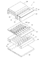
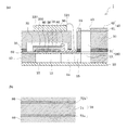
図1は、本発明の実施形態1に係る液体噴射ヘッドの一例であるインクジェット式記録ヘッドの概略構成を示す分解斜視図であり、図2は、図1の平面図であり、図3(a)は図2のA−A′線断面図、図3(b)は図3(a)の要部拡大図である。図1〜図3に示すように、本実施形態の流路形成基板10は、シリコン単結晶基板からなり、その一方の面には二酸化シリコンからなる弾性膜50が形成されている。
(1−x)[Bi(Fe1−a,Mna)O3]−x[BaTiO3] (1)
(0<x<0.40、0.01<a<0.10)
(1−y)[Bi(Fe1−b,Mnb)O3]−y[BaTiO3] (2)
(x+0.10≦y<1、0.01<b<0.10)
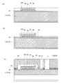
まず、単結晶シリコン(Si)基板の表面に熱酸化により酸化シリコン(SiO2)膜を形成した。次に、SiO2膜上にスパッタ法によりジルコニウム膜を作製し、熱酸化することで酸化ジルコニウム膜を形成した。次に、酸化ジルコニウム膜上に厚さ40nmの酸化チタンを積層し、その上にスパッタ法により、(111)面に配向し厚さ100nmの白金膜(第1電極60)を形成した。
白金膜(第1電極60)上に第2の圧電体層72aを形成する際の塗布工程、乾燥工程及び脱脂工程からなる工程を1回とすることにより白金膜(第1電極60)上に形成する第2の圧電体層72aの厚さを60nmとし、第1の圧電体層74上に第2の圧電体層72bを形成する際の塗布工程、乾燥工程及び脱脂工程からなる工程を1回として第1の圧電体層74上に形成する第2の圧電体層72bの厚さを60nmとし、また、第1の圧電体層74を形成する際に塗布工程、乾燥工程及び脱脂工程を2回繰り返した後に一括して焼成する焼成工程を行う工程を5回繰り返し計10回の塗布とし、第1電極60側から順に、0.65[Bi(Fe0.95,Mn0.05)O3]−0.35[BaTiO3]で表される混晶からなる複合酸化物で構成され厚さ60nmの第2の圧電体層72a、0.75[Bi(Fe0.95,Mn0.05)O3]−0.25[BaTiO3]で表される混晶からなる複合酸化物で構成され厚さ600nmの第1の圧電体層74、及び、0.65[Bi(Fe0.95,Mn0.05)O3]−0.35[BaTiO3]で表される混晶からなる複合酸化物で構成され厚さ60nmの第2の圧電体層72bを有する圧電体層70とした以外は、実施例1と同様の操作を行った。
第1の圧電体層74上に第2の圧電体層72bを形成せず、また、第1の圧電体層74を形成する際に塗布工程、乾燥工程及び脱脂工程を2回繰り返した後に一括して焼成する焼成工程を行う工程を5回繰り返し計10回の塗布とし、第1電極60側から順に、0.65[Bi(Fe0.95,Mn0.05)O3]−0.35[BaTiO3]で表される混晶からなる複合酸化物で構成され厚さ120nmの第2の圧電体層72a、及び、0.75[Bi(Fe0.95,Mn0.05)O3]−0.25[BaTiO3]で表される混晶からなる複合酸化物で構成され厚さ600nmの第1の圧電体層74を有する圧電体層70とした以外は、実施例1と同様の操作を行った。
第1電極60上及び第1の圧電体層74上に、第2の圧電体層72a及び第2の圧電体層72bを形成せず、第1の圧電体層74を形成する際に塗布工程、乾燥工程及び脱脂工程を2回繰り返した後に一括して焼成する焼成工程を行う工程を6回繰り返し計12回の塗布とし、0.75[Bi(Fe0.95,Mn0.05)O3]−0.25[BaTiO3]で表される混晶からなる複合酸化物で構成され厚さ720nmの第1の圧電体層74を有する圧電体層70とした以外は、実施例1と同様の操作を行った。
実施例1〜3及び比較例1の各圧電素子について、Bruker AXS社製の「D8 Discover」を用い、X線源にCuKα線を使用し、室温(25℃)で、圧電体層70のX線回折パターンを求めた。結果を図9に示す。この結果、実施例1〜3及び比較例1全てにおいて、鉄酸マンガン酸ビスマスや、チタン酸バリウムは、単独では検出されなかった。また、実施例1〜3及び比較例1全てにおいて、ペロブスカイト型構造に起因するピークと基板由来のピークが観測され、第2の圧電体層72a及び72bの厚さや位置を変えてもパイロクロア相等の異相由来のピークが観察されず、ペロブスカイト単相であった。
実施例1〜3及び比較例1の各圧電素子について、J−E Curveを、ヒューレットパッカード社製「4140B」を用い、室温で測定した。20V、30V及び40Vの電圧を印加した時のリーク電流値を、表1に示す。また、圧電素子が破壊した電圧である耐圧値も、表1に示す。

以上、本発明の一実施形態を説明したが、本発明の基本的構成は上述したものに限定されるものではない。例えば、上述した実施形態では、流路形成基板10として、シリコン単結晶基板を例示したが、特にこれに限定されず、例えば、SOI基板、ガラス等の材料を用いるようにしてもよい。
Claims (6)
- ノズル開口に連通する圧力発生室と、
第1電極、前記第1電極上に設けられた圧電体層および前記圧電体層上に設けられた第2電極を備えた圧電素子と、を具備し、
前記圧電体層は、鉄酸マンガン酸ビスマスとチタン酸バリウムを含む混晶として表される複合酸化物からなり、
前記圧電体層は、第1の圧電体層と、前記第1電極及び前記第2電極の少なくとも一方と前記第1の圧電体層との間に設けられ前記第1の圧電体層よりも前記チタン酸バリウムの含有量が10モル%以上多い第2の圧電体層と、を有することを特徴とする液体噴射ヘッド。 - 前記第2の圧電体層は、前記第1電極と前記第1の圧電体層との間、及び、前記第2電極と前記第1の圧電体層との間に設けられていることを特徴とする請求項1に記載する液体噴射ヘッド。
- 前記第2の圧電体層の厚さは、100nm以上であることを特徴とする請求項1又は2に記載する液体噴射ヘッド。
- 前記第1の圧電体層は下記式(1)で表される混晶からなる複合酸化物であり、前記第2の圧電体層は下記式(2)で表される混晶からなる複合酸化物であることを特徴とする請求項1〜3のいずれか一項に記載する液体噴射ヘッド。
(1−x)[Bi(Fe1−a,Mna)O3]−x[BaTiO3] (1)
(0<x<0.40、0.01<a<0.10)
(1−y)[Bi(Fe1−b,Mnb)O3]−y[BaTiO3] (2)
(x+0.10≦y<1、0.01<b<0.10) - 請求項1〜4のいずれか一項に記載する液体噴射ヘッドを具備することを特徴とする液体噴射装置。
- 第1電極と、前記第1電極上に設けられた圧電体層と、前記圧電体層上に設けられた第2電極とを備え、
前記圧電体層は、鉄酸マンガン酸ビスマスとチタン酸バリウムを含む混晶として表される複合酸化物からなり、
前記圧電体層は、第1の圧電体層と、前記第1電極及び前記第2電極の少なくとも一方と前記第1の圧電体層との間に設けられ前記第1の圧電体層よりもチタン酸バリウムの含有量が10モル%以上多い第2の圧電体層と、を有することを特徴とする圧電素子。
Priority Applications (2)
| Application Number | Priority Date | Filing Date | Title |
|---|---|---|---|
| JP2011025460A JP5773129B2 (ja) | 2011-02-08 | 2011-02-08 | 液体噴射ヘッド、液体噴射装置、圧電素子、超音波デバイス及びirセンサー |
| US13/363,501 US8567927B2 (en) | 2011-02-08 | 2012-02-01 | Piezoelectric device, liquid-ejecting head, and liquid-ejecting apparatus |
Applications Claiming Priority (1)
| Application Number | Priority Date | Filing Date | Title |
|---|---|---|---|
| JP2011025460A JP5773129B2 (ja) | 2011-02-08 | 2011-02-08 | 液体噴射ヘッド、液体噴射装置、圧電素子、超音波デバイス及びirセンサー |
Publications (3)
| Publication Number | Publication Date |
|---|---|
| JP2012164894A true JP2012164894A (ja) | 2012-08-30 |
| JP2012164894A5 JP2012164894A5 (ja) | 2014-03-27 |
| JP5773129B2 JP5773129B2 (ja) | 2015-09-02 |
Family
ID=46600382
Family Applications (1)
| Application Number | Title | Priority Date | Filing Date |
|---|---|---|---|
| JP2011025460A Expired - Fee Related JP5773129B2 (ja) | 2011-02-08 | 2011-02-08 | 液体噴射ヘッド、液体噴射装置、圧電素子、超音波デバイス及びirセンサー |
Country Status (2)
| Country | Link |
|---|---|
| US (1) | US8567927B2 (ja) |
| JP (1) | JP5773129B2 (ja) |
Cited By (1)
| Publication number | Priority date | Publication date | Assignee | Title |
|---|---|---|---|---|
| JP2017108125A (ja) * | 2015-11-27 | 2017-06-15 | キヤノン株式会社 | 圧電素子、圧電素子の製造方法、圧電アクチュエータおよび電子機器 |
Families Citing this family (4)
| Publication number | Priority date | Publication date | Assignee | Title |
|---|---|---|---|---|
| JP5278654B2 (ja) * | 2008-01-24 | 2013-09-04 | セイコーエプソン株式会社 | 液体噴射ヘッド及び液体噴射装置 |
| JP5825466B2 (ja) * | 2011-02-24 | 2015-12-02 | セイコーエプソン株式会社 | 液体噴射ヘッド及び液体噴射装置並びに圧電素子 |
| JP6296227B2 (ja) * | 2013-11-22 | 2018-03-20 | セイコーエプソン株式会社 | 液体噴射ヘッド、液体噴射装置及び圧電素子 |
| KR102589839B1 (ko) * | 2020-12-24 | 2023-10-16 | 삼성전기주식회사 | 체적 음향 공진기 및 그 제조 방법 |
Citations (3)
| Publication number | Priority date | Publication date | Assignee | Title |
|---|---|---|---|---|
| JP2006032628A (ja) * | 2004-07-15 | 2006-02-02 | Seiko Epson Corp | 圧電素子、圧電アクチュエーター、圧電ポンプ、インクジェット式記録ヘッド、インクジェットプリンター、表面弾性波素子、周波数フィルタ、発振器、電子回路、薄膜圧電共振器、および電子機器 |
| JP2008028285A (ja) * | 2006-07-25 | 2008-02-07 | Matsushita Electric Ind Co Ltd | 圧電体薄膜素子、インクジェットヘッドおよびインクジェット式記録装置 |
| JP2009252790A (ja) * | 2008-04-01 | 2009-10-29 | Seiko Epson Corp | 圧電材料および圧電素子 |
Family Cites Families (5)
| Publication number | Priority date | Publication date | Assignee | Title |
|---|---|---|---|---|
| JP4051654B2 (ja) | 2000-02-08 | 2008-02-27 | セイコーエプソン株式会社 | 圧電体素子、インクジェット式記録ヘッド及びこれらの製造方法並びにインクジェットプリンタ |
| JP5345868B2 (ja) | 2008-03-31 | 2013-11-20 | 富士フイルム株式会社 | ペロブスカイト型酸化物膜、強誘電体、圧電素子、液体吐出装置 |
| JP5248168B2 (ja) | 2008-04-01 | 2013-07-31 | セイコーエプソン株式会社 | 圧電材料および圧電素子 |
| JP5313792B2 (ja) | 2008-07-17 | 2013-10-09 | 富士フイルム株式会社 | ペロブスカイト型酸化物、酸化物組成物、酸化物体、圧電素子、及び液体吐出装置 |
| JP2011222849A (ja) * | 2010-04-13 | 2011-11-04 | Seiko Epson Corp | 液体噴射ヘッド、液体噴射装置、および圧電素子 |
-
2011
- 2011-02-08 JP JP2011025460A patent/JP5773129B2/ja not_active Expired - Fee Related
-
2012
- 2012-02-01 US US13/363,501 patent/US8567927B2/en not_active Expired - Fee Related
Patent Citations (3)
| Publication number | Priority date | Publication date | Assignee | Title |
|---|---|---|---|---|
| JP2006032628A (ja) * | 2004-07-15 | 2006-02-02 | Seiko Epson Corp | 圧電素子、圧電アクチュエーター、圧電ポンプ、インクジェット式記録ヘッド、インクジェットプリンター、表面弾性波素子、周波数フィルタ、発振器、電子回路、薄膜圧電共振器、および電子機器 |
| JP2008028285A (ja) * | 2006-07-25 | 2008-02-07 | Matsushita Electric Ind Co Ltd | 圧電体薄膜素子、インクジェットヘッドおよびインクジェット式記録装置 |
| JP2009252790A (ja) * | 2008-04-01 | 2009-10-29 | Seiko Epson Corp | 圧電材料および圧電素子 |
Non-Patent Citations (1)
| Title |
|---|
| JPN6014013159; Serhiy O. LEONTSEV(他1名): 'Dielectric and Piezoelectric Properties in Mn-Modified (1-x)BiFeO3-xBaTiO3 Ceramics' Journal of the American Ceramic Society Volume 92, Issue 12, 200912, p.2957-2961, The American Ceramic Society * |
Cited By (1)
| Publication number | Priority date | Publication date | Assignee | Title |
|---|---|---|---|---|
| JP2017108125A (ja) * | 2015-11-27 | 2017-06-15 | キヤノン株式会社 | 圧電素子、圧電素子の製造方法、圧電アクチュエータおよび電子機器 |
Also Published As
| Publication number | Publication date |
|---|---|
| JP5773129B2 (ja) | 2015-09-02 |
| US20120200643A1 (en) | 2012-08-09 |
| US8567927B2 (en) | 2013-10-29 |
Similar Documents
| Publication | Publication Date | Title |
|---|---|---|
| JP5672433B2 (ja) | 液体噴射ヘッド、液体噴射装置、圧電素子、焦電素子及びirセンサー | |
| JP5668473B2 (ja) | 圧電素子及びその製造方法、液体噴射ヘッド、液体噴射装置、超音波センサー、並びに赤外線センサー | |
| JP5429492B2 (ja) | 液体噴射ヘッド、液体噴射装置、圧電素子及びアクチュエーター装置 | |
| JP5812243B2 (ja) | 液体噴射ヘッド、液体噴射装置、圧電素子、超音波デバイス及びirセンサー | |
| JP5773129B2 (ja) | 液体噴射ヘッド、液体噴射装置、圧電素子、超音波デバイス及びirセンサー | |
| JP2011211143A (ja) | 液体噴射ヘッド及び液体噴射装置並びに圧電素子 | |
| JP2012139919A (ja) | 液体噴射ヘッドの製造方法、液体噴射装置、及び圧電素子の製造方法 | |
| JP5534197B2 (ja) | 液体噴射ヘッド、液体噴射装置、圧電素子及び焦電センサー | |
| JP5740951B2 (ja) | 液体噴射ヘッド、液体噴射装置、圧電素子、赤外線センサー及び超音波センサー | |
| JP6146599B2 (ja) | 圧電素子、液体噴射ヘッド、液体噴射装置、超音波デバイス及びセンサー | |
| JP5884959B2 (ja) | 圧電体膜の製造方法、圧電素子及び液体噴射ヘッド並びに液体噴射装置 | |
| JP2013131572A (ja) | 液体噴射ヘッド、液体噴射装置及び圧電素子 | |
| JP5585197B2 (ja) | 液体噴射ヘッド及び液体噴射装置並びに圧電素子 | |
| JP2011238708A (ja) | 液体噴射ヘッドの製造方法、液体噴射装置、及び圧電素子の製造方法 | |
| JP5790922B2 (ja) | 圧電素子、液体噴射ヘッド、液体噴射装置、超音波デバイス及びセンサー | |
| JP5880821B2 (ja) | 液体噴射ヘッド、液体噴射装置、及び圧電素子 | |
| JP5773127B2 (ja) | 液体噴射ヘッド、液体噴射装置、圧電素子、超音波デバイス及びirセンサー | |
| JP2015061048A (ja) | 液体噴射ヘッド、液体噴射装置及び圧電素子 | |
| JP2014194992A (ja) | 液体噴射ヘッド及び液体噴射装置並びに圧電素子 | |
| JP2011192951A (ja) | 液体噴射ヘッド及び液体噴射装置 | |
| JP5765525B2 (ja) | 液体噴射ヘッド、液体噴射装置、圧電素子、超音波デバイス及びirセンサー | |
| JP5892308B2 (ja) | 液体噴射ヘッド及び液体噴射装置並びに圧電素子 | |
| JP2013165195A (ja) | 液体噴射ヘッド、液体噴射装置及び圧電素子 | |
| JP2013080882A (ja) | 液体噴射ヘッドの製造方法、液体噴射装置の製造方法及び圧電素子の製造方法 | |
| JP2013055276A (ja) | 液体噴射ヘッド及び液体噴射装置並びに圧電素子 |
Legal Events
| Date | Code | Title | Description |
|---|---|---|---|
| A521 | Request for written amendment filed |
Free format text: JAPANESE INTERMEDIATE CODE: A523 Effective date: 20140206 |
|
| A621 | Written request for application examination |
Free format text: JAPANESE INTERMEDIATE CODE: A621 Effective date: 20140206 |
|
| A977 | Report on retrieval |
Free format text: JAPANESE INTERMEDIATE CODE: A971007 Effective date: 20150115 |
|
| A131 | Notification of reasons for refusal |
Free format text: JAPANESE INTERMEDIATE CODE: A131 Effective date: 20150204 |
|
| A521 | Request for written amendment filed |
Free format text: JAPANESE INTERMEDIATE CODE: A523 Effective date: 20150406 |
|
| RD04 | Notification of resignation of power of attorney |
Free format text: JAPANESE INTERMEDIATE CODE: A7424 Effective date: 20150422 |
|
| TRDD | Decision of grant or rejection written | ||
| A01 | Written decision to grant a patent or to grant a registration (utility model) |
Free format text: JAPANESE INTERMEDIATE CODE: A01 Effective date: 20150603 |
|
| A61 | First payment of annual fees (during grant procedure) |
Free format text: JAPANESE INTERMEDIATE CODE: A61 Effective date: 20150616 |
|
| R150 | Certificate of patent or registration of utility model |
Ref document number: 5773129 Country of ref document: JP Free format text: JAPANESE INTERMEDIATE CODE: R150 |
|
| S531 | Written request for registration of change of domicile |
Free format text: JAPANESE INTERMEDIATE CODE: R313531 |
|
| R350 | Written notification of registration of transfer |
Free format text: JAPANESE INTERMEDIATE CODE: R350 |
|
| LAPS | Cancellation because of no payment of annual fees |