JP2012175441A - 半導体装置 - Google Patents
半導体装置 Download PDFInfo
- Publication number
- JP2012175441A JP2012175441A JP2011036041A JP2011036041A JP2012175441A JP 2012175441 A JP2012175441 A JP 2012175441A JP 2011036041 A JP2011036041 A JP 2011036041A JP 2011036041 A JP2011036041 A JP 2011036041A JP 2012175441 A JP2012175441 A JP 2012175441A
- Authority
- JP
- Japan
- Prior art keywords
- bias
- line
- circuit
- semiconductor device
- control signal
- Prior art date
- Legal status (The legal status is an assumption and is not a legal conclusion. Google has not performed a legal analysis and makes no representation as to the accuracy of the status listed.)
- Pending
Links
- 239000004065 semiconductor Substances 0.000 title claims abstract description 25
- 230000003071 parasitic effect Effects 0.000 claims abstract description 11
- 230000008859 change Effects 0.000 claims abstract description 9
- 239000003990 capacitor Substances 0.000 claims description 26
- 230000005540 biological transmission Effects 0.000 claims description 14
- 238000006243 chemical reaction Methods 0.000 claims description 3
- 238000010586 diagram Methods 0.000 description 14
- 238000001514 detection method Methods 0.000 description 6
- 230000004913 activation Effects 0.000 description 2
- 230000003111 delayed effect Effects 0.000 description 2
- 230000003213 activating effect Effects 0.000 description 1
- 230000000052 comparative effect Effects 0.000 description 1
- 230000007423 decrease Effects 0.000 description 1
- 230000001934 delay Effects 0.000 description 1
- 230000006870 function Effects 0.000 description 1
- 230000004048 modification Effects 0.000 description 1
- 238000012986 modification Methods 0.000 description 1
- 230000004044 response Effects 0.000 description 1
Images


Classifications
-
- H—ELECTRICITY
- H02—GENERATION; CONVERSION OR DISTRIBUTION OF ELECTRIC POWER
- H02M—APPARATUS FOR CONVERSION BETWEEN AC AND AC, BETWEEN AC AND DC, OR BETWEEN DC AND DC, AND FOR USE WITH MAINS OR SIMILAR POWER SUPPLY SYSTEMS; CONVERSION OF DC OR AC INPUT POWER INTO SURGE OUTPUT POWER; CONTROL OR REGULATION THEREOF
- H02M7/00—Conversion of AC power input into DC power output; Conversion of DC power input into AC power output
- H02M7/003—Constructional details, e.g. physical layout, assembly, wiring or busbar connections
-
- H—ELECTRICITY
- H03—ELECTRONIC CIRCUITRY
- H03K—PULSE TECHNIQUE
- H03K19/00—Logic circuits, i.e. having at least two inputs acting on one output; Inverting circuits
- H03K19/003—Modifications for increasing the reliability for protection
- H03K19/00346—Modifications for eliminating interference or parasitic voltages or currents
- H03K19/00361—Modifications for eliminating interference or parasitic voltages or currents in field effect transistor circuits
Landscapes
- Engineering & Computer Science (AREA)
- Power Engineering (AREA)
- Dram (AREA)
- Pulse Circuits (AREA)
- Logic Circuits (AREA)
Abstract
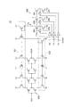
【解決手段】バイアス電流が流れるバイアスラインVLと、バイアス電流の量を制御信号DDに基づいて切り替える切り替えスイッチ70と、制御信号DDが供給される制御ラインとバイアスラインVLとの間の寄生容量を介して制御信号DDの変化時に生じるバイアスラインVLの電位変動を相殺する相殺回路91〜93とを備える。本発明によれば、切り替えスイッチ70のオンオフに伴ってバイアスラインVLに生じるノイズを相殺することが可能となる。
【選択図】図5
Description
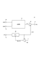
11 主回路
12 出力バッファ
13 データ出力端子
14 アドレス端子
15 コマンド端子
16 クロック端子
20 DLL回路
21 ディレイライン
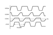
22 デューティ調整回路
23 位相検出回路
24 カウンタ回路
25 デューティ検出回路
26 バイアス回路
30 レプリカバッファ
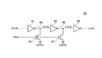
41〜43 インバータ
44,46 クロック伝送ライン
45,47 バイアストランジスタ
50 バイアス源
51,53 トランジスタ
52 抵抗
60 電流源
61〜63 トランジスタ
70 切り替えスイッチ
71〜73 トランジスタ
80 電流電圧変換回路
81 補償容量
91〜93 バランス容量(相殺回路)
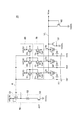
220 インバータ列
231,232 定電流回路
240 電流調整回路
241〜243 選択トランジスタ
291〜293 バランス容量(相殺回路)
VL バイアスライン
Claims (10)
- バイアス電流が流れるバイアスラインと、
前記バイアス電流の量を制御信号に基づいて切り替える切り替えスイッチと、
前記制御信号が供給される制御ラインと、
前記制御ラインと前記バイアスラインとの間の寄生容量を介して前記制御信号の変化時に生じる前記バイアスラインの電位変動を相殺する相殺回路と、を備えることを特徴とする半導体装置。 - 前記相殺回路は、一端が前記バイアスラインに接続され、他端に前記制御信号の反転信号が供給されるバランス容量を含むことを特徴とする請求項1に記載の半導体装置。
- 前記切り替えスイッチはMOSトランジスタからなり、前記寄生容量は前記切り替えスイッチを構成するMOSトランジスタのゲートドレイン間容量からなることを特徴とする請求項2に記載の半導体装置。
- 前記バランス容量はソースとドレインが短絡されたMOSトランジスタからなることを特徴とする請求項3に記載の半導体装置。
- 前記バランス容量を構成するMOSトランジスタのゲート面積は、前記切り替えスイッチを構成するMOSトランジスタのゲート面積の半分であることを特徴とする請求項4に記載の半導体装置。
- 前記バイアス電流をバイアス電圧に変換する電流電圧変換回路と、前記バイアス電圧が制御電極に供給されるバイアストランジスタとをさらに備えることを特徴とする請求項1乃至5のいずれか一項に記載の半導体装置。
- クロック信号を伝送するクロック伝送ラインをさらに備え、前記バイアストランジスタは前記クロック伝送ラインに接続され、これにより前記バイアス電圧に応じて前記クロック伝送ラインの伝送特性が変化することを特徴とする請求項6に記載の半導体装置。
- クロック信号を伝送するインバータ列をさらに備え、前記バイアストランジスタは前記インバータ列を構成するトランジスタと電源ラインとの間に挿入され、これにより前記バイアス電圧に応じて前記インバータ列の伝送特性が変化することを特徴とする請求項6に記載の半導体装置。
- バイアス電流が流れるバイアスラインと、
ゲート幅が互いに異なり、ドレインが前記バイアスラインに共通接続された複数のMOSトランジスタからなる切り替えスイッチと、
前記複数のMOSトランジスタのゲートにそれぞれ個別の制御信号を供給する制御回路と、
容量値が互いに異なり、一端が前記バイアスラインに共通接続され、他端にそれぞれ対応する前記制御信号の反転信号が供給される複数のバランス容量と、を備えることを特徴とする半導体装置。 - ゲートに所定の制御信号が供給されるMOSトランジスタのゲートドレイン間容量は、前記所定の制御信号の反転信号が供給されるバランス容量の容量値と等しいことを特徴とする請求項9に記載の半導体装置。
Priority Applications (3)
| Application Number | Priority Date | Filing Date | Title |
|---|---|---|---|
| JP2011036041A JP2012175441A (ja) | 2011-02-22 | 2011-02-22 | 半導体装置 |
| US13/398,711 US8665008B2 (en) | 2011-02-22 | 2012-02-16 | Semiconductor device that can cancel noise in bias line to which bias current flows |
| US14/174,670 US9379600B2 (en) | 2011-02-22 | 2014-02-06 | Semiconductor device that can cancel noise in bias line to which bias current flows |
Applications Claiming Priority (1)
| Application Number | Priority Date | Filing Date | Title |
|---|---|---|---|
| JP2011036041A JP2012175441A (ja) | 2011-02-22 | 2011-02-22 | 半導体装置 |
Publications (1)
| Publication Number | Publication Date |
|---|---|
| JP2012175441A true JP2012175441A (ja) | 2012-09-10 |
Family
ID=46652252
Family Applications (1)
| Application Number | Title | Priority Date | Filing Date |
|---|---|---|---|
| JP2011036041A Pending JP2012175441A (ja) | 2011-02-22 | 2011-02-22 | 半導体装置 |
Country Status (2)
| Country | Link |
|---|---|
| US (2) | US8665008B2 (ja) |
| JP (1) | JP2012175441A (ja) |
Cited By (3)
| Publication number | Priority date | Publication date | Assignee | Title |
|---|---|---|---|---|
| JP2016525301A (ja) * | 2013-06-25 | 2016-08-22 | クゥアルコム・インコーポレイテッドQualcomm Incorporated | フィードバックループ内にデューティサイクル調整を有する分周器 |
| JP2016184918A (ja) * | 2015-03-26 | 2016-10-20 | パナソニック株式会社 | スイッチ制御回路 |
| JP2018186376A (ja) * | 2017-04-25 | 2018-11-22 | 新日本無線株式会社 | 増幅回路 |
Families Citing this family (5)
| Publication number | Priority date | Publication date | Assignee | Title |
|---|---|---|---|---|
| US9484601B2 (en) * | 2013-07-30 | 2016-11-01 | Elwha Llc | Load-managed electrochemical energy generation system |
| US8729959B1 (en) * | 2013-08-09 | 2014-05-20 | Issc Technologies Corp. | Voltage generating apparatus |
| KR20160076197A (ko) * | 2014-12-22 | 2016-06-30 | 에스케이하이닉스 주식회사 | 듀티 싸이클 감지 회로 및 이를 포함하는 반도체 장치 |
| KR20180045677A (ko) * | 2016-10-26 | 2018-05-04 | 에스케이하이닉스 주식회사 | 수신 장치, 전송 장치, 이를 이용하는 반도체 장치 및 시스템 |
| US12431099B1 (en) * | 2024-09-26 | 2025-09-30 | Apple Inc. | Charge cancellation to minimize transient ripple |
Citations (2)
| Publication number | Priority date | Publication date | Assignee | Title |
|---|---|---|---|---|
| JP2008072361A (ja) * | 2006-09-13 | 2008-03-27 | Matsushita Electric Ind Co Ltd | Ad変換器およびデルタシグマad変換器 |
| JP2009118049A (ja) * | 2007-11-05 | 2009-05-28 | Panasonic Corp | 離散時間型増幅回路及びアナログ・ディジタル変換器 |
Family Cites Families (9)
| Publication number | Priority date | Publication date | Assignee | Title |
|---|---|---|---|---|
| JPS584491B2 (ja) | 1978-11-08 | 1983-01-26 | 日本電信電話株式会社 | 半導体アナログスイツチ |
| JPS5894232A (ja) | 1981-11-30 | 1983-06-04 | Toshiba Corp | 半導体アナログスイッチ回路 |
| JP3307453B2 (ja) * | 1993-03-18 | 2002-07-24 | ソニー株式会社 | 昇圧回路 |
| JP3550868B2 (ja) | 1996-04-16 | 2004-08-04 | 株式会社日立製作所 | 可変遅延回路 |
| JP2001326562A (ja) * | 2000-05-15 | 2001-11-22 | Nec Corp | 可変遅延回路 |
| US7173457B2 (en) * | 2005-01-31 | 2007-02-06 | Kabushiki Kaisha Toshiba | Silicon-on-insulator sense amplifier for memory cell |
| KR100891300B1 (ko) * | 2007-09-04 | 2009-04-06 | 주식회사 하이닉스반도체 | 반도체 장치 및 그 구동방법 |
| US7944262B2 (en) | 2008-05-21 | 2011-05-17 | Elpida Memory, Inc. | Duty correction circuit |
| US7952408B2 (en) * | 2009-06-26 | 2011-05-31 | University Of Florida Research Foundation, Inc. | Embedded phase noise measurement system |
-
2011
- 2011-02-22 JP JP2011036041A patent/JP2012175441A/ja active Pending
-
2012
- 2012-02-16 US US13/398,711 patent/US8665008B2/en active Active
-
2014
- 2014-02-06 US US14/174,670 patent/US9379600B2/en active Active
Patent Citations (2)
| Publication number | Priority date | Publication date | Assignee | Title |
|---|---|---|---|---|
| JP2008072361A (ja) * | 2006-09-13 | 2008-03-27 | Matsushita Electric Ind Co Ltd | Ad変換器およびデルタシグマad変換器 |
| JP2009118049A (ja) * | 2007-11-05 | 2009-05-28 | Panasonic Corp | 離散時間型増幅回路及びアナログ・ディジタル変換器 |
Cited By (3)
| Publication number | Priority date | Publication date | Assignee | Title |
|---|---|---|---|---|
| JP2016525301A (ja) * | 2013-06-25 | 2016-08-22 | クゥアルコム・インコーポレイテッドQualcomm Incorporated | フィードバックループ内にデューティサイクル調整を有する分周器 |
| JP2016184918A (ja) * | 2015-03-26 | 2016-10-20 | パナソニック株式会社 | スイッチ制御回路 |
| JP2018186376A (ja) * | 2017-04-25 | 2018-11-22 | 新日本無線株式会社 | 増幅回路 |
Also Published As
| Publication number | Publication date |
|---|---|
| US20120212286A1 (en) | 2012-08-23 |
| US8665008B2 (en) | 2014-03-04 |
| US9379600B2 (en) | 2016-06-28 |
| US20140152380A1 (en) | 2014-06-05 |
Similar Documents
| Publication | Publication Date | Title |
|---|---|---|
| JP2012175441A (ja) | 半導体装置 | |
| KR100646940B1 (ko) | 낮은 첨두 전류치를 가지는 리프레시 제어기 | |
| US8248864B2 (en) | Semiconductor memory device | |
| US20080303558A1 (en) | Data output driver circuit | |
| US8547138B2 (en) | Semiconductor device with buffer and replica circuits | |
| US12388438B2 (en) | Semiconductor integrated circuit device and semiconductor system including the same | |
| KR100680441B1 (ko) | 안정적인 승압 전압을 발생하는 승압 전압 발생기 | |
| US7994835B2 (en) | Duty control circuit and semiconductor device having the same | |
| JP2004135098A (ja) | 出力データのスルーレート制御方式 | |
| JP5677205B2 (ja) | 半導体記憶装置 | |
| US7362167B2 (en) | Voltage generator | |
| US8331165B2 (en) | Semiconductor device | |
| KR20000018628A (ko) | 부하 적응형 저잡음 출력버퍼 | |
| US20070216450A1 (en) | Semiconductor integrated circuit device and semiconductor integrated circuit system | |
| US10340857B2 (en) | Amplifier circuit | |
| JP2015002452A (ja) | 半導体装置 | |
| JP6540290B2 (ja) | レベルコンバータ回路 | |
| US8829969B2 (en) | Level-down shifter | |
| JPWO2012153517A1 (ja) | 半導体集積回路 | |
| KR100849957B1 (ko) | 반도체 메모리 장치 및 그것의 입출력 구동회로 및 그것에대한 전류 공급 방법 | |
| KR20090114959A (ko) | 반도체 소자의 출력 드라이버 | |
| US7746122B2 (en) | Input buffer for semiconductor memory apparatus | |
| KR101049705B1 (ko) | 신호 출력 회로 및 그것을 이용한 선택기 회로 | |
| KR20090048888A (ko) | 반도체 메모리 장치의 듀티 보정 회로 | |
| US20110090000A1 (en) | Signal transmission circuit |
Legal Events
| Date | Code | Title | Description |
|---|---|---|---|
| A711 | Notification of change in applicant |
Free format text: JAPANESE INTERMEDIATE CODE: A711 Effective date: 20131029 |
|
| A711 | Notification of change in applicant |
Free format text: JAPANESE INTERMEDIATE CODE: A711 Effective date: 20131030 |
|
| A621 | Written request for application examination |
Free format text: JAPANESE INTERMEDIATE CODE: A621 Effective date: 20140205 |
|
| A977 | Report on retrieval |
Free format text: JAPANESE INTERMEDIATE CODE: A971007 Effective date: 20140501 |
|
| A131 | Notification of reasons for refusal |
Free format text: JAPANESE INTERMEDIATE CODE: A131 Effective date: 20140513 |
|
| A521 | Request for written amendment filed |
Free format text: JAPANESE INTERMEDIATE CODE: A523 Effective date: 20140812 |
|
| A02 | Decision of refusal |
Free format text: JAPANESE INTERMEDIATE CODE: A02 Effective date: 20140924 |
|
| A601 | Written request for extension of time |
Free format text: JAPANESE INTERMEDIATE CODE: A601 Effective date: 20151117 |
|
| A521 | Request for written amendment filed |
Free format text: JAPANESE INTERMEDIATE CODE: A523 Effective date: 20160225 |
|
| A601 | Written request for extension of time |
Free format text: JAPANESE INTERMEDIATE CODE: A601 Effective date: 20160725 |