JP2012178332A - Display device - Google Patents
Display device Download PDFInfo
- Publication number
- JP2012178332A JP2012178332A JP2011260906A JP2011260906A JP2012178332A JP 2012178332 A JP2012178332 A JP 2012178332A JP 2011260906 A JP2011260906 A JP 2011260906A JP 2011260906 A JP2011260906 A JP 2011260906A JP 2012178332 A JP2012178332 A JP 2012178332A
- Authority
- JP
- Japan
- Prior art keywords
- organic
- lens
- layer
- light
- resin
- Prior art date
- Legal status (The legal status is an assumption and is not a legal conclusion. Google has not performed a legal analysis and makes no representation as to the accuracy of the status listed.)
- Pending
Links
Images
Classifications
-
- H—ELECTRICITY
- H10—SEMICONDUCTOR DEVICES; ELECTRIC SOLID-STATE DEVICES NOT OTHERWISE PROVIDED FOR
- H10K—ORGANIC ELECTRIC SOLID-STATE DEVICES
- H10K59/00—Integrated devices, or assemblies of multiple devices, comprising at least one organic light-emitting element covered by group H10K50/00
- H10K59/80—Constructional details
- H10K59/875—Arrangements for extracting light from the devices
- H10K59/879—Arrangements for extracting light from the devices comprising refractive means, e.g. lenses
-
- H—ELECTRICITY
- H10—SEMICONDUCTOR DEVICES; ELECTRIC SOLID-STATE DEVICES NOT OTHERWISE PROVIDED FOR
- H10K—ORGANIC ELECTRIC SOLID-STATE DEVICES
- H10K50/00—Organic light-emitting devices
- H10K50/80—Constructional details
- H10K50/85—Arrangements for extracting light from the devices
- H10K50/858—Arrangements for extracting light from the devices comprising refractive means, e.g. lenses
Landscapes
- Physics & Mathematics (AREA)
- Optics & Photonics (AREA)
- Electroluminescent Light Sources (AREA)
Abstract
Description
有機EL素子を備えた表示装置に関する。 The present invention relates to a display device including an organic EL element.
近年、有機EL素子を備えた表示装置に関して盛んに研究開発されている。有機EL素子は陽極と発光層を含む有機化合物層と陰極とで構成され、陽極と陰極からそれぞれ正孔と電子が発光層に注入され、正孔と電子の再結合エネルギーを利用して発光層から光が出射される。 In recent years, active research and development have been conducted on display devices including organic EL elements. An organic EL element is composed of an anode, an organic compound layer including a light emitting layer, and a cathode, and holes and electrons are injected into the light emitting layer from the anode and the cathode, respectively, and the light emitting layer utilizes recombination energy of holes and electrons. The light is emitted from.
有機EL素子の課題として、光取り出し効率の向上が挙げられる。この課題を解決するために、特許文献1では、有機EL素子の発光面側にレンズアレイを設ける構成が示されている。 As a problem of the organic EL element, improvement of light extraction efficiency can be mentioned. In order to solve this problem, Patent Document 1 discloses a configuration in which a lens array is provided on the light emitting surface side of an organic EL element.
しかし、特許文献1で示される有機EL素子においては、発光光を集光して斜めに出射する光を正面方向に集めるため、正面の輝度は改善されるが、斜め方向における輝度が著しく低下し、視野角が小さくなるという課題があった。 However, in the organic EL element disclosed in Patent Document 1, since the emitted light is collected and the light emitted obliquely is collected in the front direction, the front luminance is improved, but the luminance in the diagonal direction is significantly reduced. There is a problem that the viewing angle becomes small.
本発明は上記課題に鑑みて、視野角特性を維持しつつ、光取り出し効率を向上させる表示装置を得ることを目的とする。 In view of the above problems, an object of the present invention is to obtain a display device that improves light extraction efficiency while maintaining viewing angle characteristics.
本発明は、有機EL素子と、有機EL素子に接して、有機EL素子を保護する保護層と、前記保護層に接して、有機EL素子の光出射側に配置される、有機EL素子の発光面に対して凸状の集光レンズと、を有し、前記集光レンズの表面、以下の式を満たす点を有することを特徴とする表示装置。
sin[θS−Arcsin{(n1/n2)×sin(θS−θ)}]≧1/n2
なお、θは前記有機EL素子から出射されて前記集光レンズの表面に入射されうる光の発光角度、θSは発光角度θで有機EL素子から出射した光が当たる前記集光レンズの表面の傾斜角度、n1は前記集光レンズの屈折率、n2は前記集光レンズの前記有機EL素子とは反対側にある媒質の屈折率である。
The present invention relates to an organic EL element, a protective layer in contact with the organic EL element and protecting the organic EL element, and light emission of the organic EL element in contact with the protective layer and disposed on the light emitting side of the organic EL element. And a condensing lens that is convex with respect to the surface, and the surface of the condensing lens has a point that satisfies the following expression.
sin [θ S −Arcsin {(n 1 / n 2 ) × sin (θ S −θ)}] ≧ 1 / n 2
Is the emission angle of light that can be emitted from the organic EL element and incident on the surface of the condenser lens, and θ S is the surface of the condenser lens that is irradiated with the light emitted from the organic EL element at the emission angle θ. The tilt angle, n 1 is the refractive index of the condenser lens, and n 2 is the refractive index of the medium on the opposite side of the condenser lens from the organic EL element.
本発明は、視野角特性を維持しつつ、光取り出し効率を向上させる表示装置を得ることができる。 The present invention can provide a display device that improves light extraction efficiency while maintaining viewing angle characteristics.
<有機EL表示装置について>
以下、本発明の実施形態に係る表示装置について、図面を参照して説明する。
<About organic EL display devices>
Hereinafter, a display device according to an embodiment of the present invention will be described with reference to the drawings.
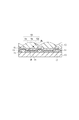
図1は、本発明の実施形態に係る表示装置を示す部分断面図である。本表示装置は、基板上に形成された有機EL素子の上面から、図1においては上方向に光を取り出すトップエミッション型の表示装置である。 FIG. 1 is a partial cross-sectional view showing a display device according to an embodiment of the present invention. This display device is a top emission type display device that extracts light upward in FIG. 1 from the upper surface of the organic EL element formed on the substrate.
本発明の表示装置は、基板10と、基板10上にマトリクス状に形成された、表示領域を構成する複数の画素からなる。ここで、画素とは、1つの発光素子に対応した領域を意味する。本発明では、発光素子としての有機EL素子が上記複数の画素のそれぞれに形成されており、それら有機EL素子間には画素間を分離する隔壁12が設けられている。また、有機EL素子の夫々は、一対の電極である陽極11及び陰極14と、それらの電極間に配置された、発光層を含む有機化合物層13(以下、有機EL層と呼称する)を備えている。具体的には、基板10の上に、画素毎にパターニングされた陽極11が形成され、その陽極11上に有機EL層13が形成され、更に、有機EL層13上に陰極14が形成されている。
The display device of the present invention includes a
陽極11は、例えば、Ag等の高い反射率を持つ導電性の金属材料から形成される。また、陽極は、そのような金属材料から成る層とホール注入特性に優れたITOやIZO(登録商標)などの透明導電性材料から成る層との積層体から構成しても良い。
The
一方、陰極14は、複数の有機EL素子に対して共通に形成されており、また、発光層で発光した光を素子外部に取り出し可能な半反射性或いは光透過性の構成を有している。具体的には、素子内部での干渉効果を高めるために陰極14を半反射性の構成とする場合、陰極14は、AgやAgMgなどの電子注入性に優れた導電性の金属材料から成る層を2乃至50nmの膜厚で形成することにより構成されている。なお、半反射性とは、素子内部で発光した光の一部を反射し、一部を透過する性質を意味し、可視光に対して20乃至80%の反射率を有するものをいう。また、光透過性とは、可視光に対して80%以上の透過率を有するものをいう。
On the other hand, the
また、有機EL層13は、少なくとも発光層を含む単層又は複数の層からなる。例えば、有機EL層13の構成例としては、正孔輸送層、発光層、電子輸送層及び電子注入層からなる4層構成や、正孔輸送層、発光層及び電子輸送層からなる3層構成等が挙げられる。有機EL層13を構成する材料は、公知の材料を使用することができる。
The
基板10には各有機EL素子を独立に駆動可能なように画素回路が形成されている。これらの画素回路は、複数のトランジスタから構成されている(不図示)。このトランジスタが形成された基板10は、トランジスタと陽極11とを電気的に接続するためのコンタクトホールが形成された層間絶縁膜に覆われている(不図示)。更に層間絶縁膜上には、画素回路による表面凹凸を吸収し、表面を平坦にするための平坦化膜が形成されている(不図示)。
A pixel circuit is formed on the
また、陰極14の上には、空気中の酸素や水分から有機EL層13を保護するために、有機EL素子に接して第1の保護層が形成されている。
Further, a first protective layer is formed on the
第1の保護層15は、酸化シリコン、窒化シリコン、酸化窒化シリコン、酸化アルミナなどの無機材料からなる。また、第1の保護層15は、後述する樹脂材料の硬化に伴い発生する応力を緩和する作用を持たせることも可能である。膜厚は0.1μm以上10μm以下が好ましく、CVD法で形成することが好ましい。なお、第1の保護層15は、上記の無機材料の単層でもよいし、異なる材料の積層膜でもよい。
The first
そして、本発明の表示装置は、第1の保護層15の上に、第1の保護層15に接して、有機EL素子の光出射側に配置される、有機EL素子の発光面に対して凸状のレンズ部16を有している。レンズ部16は、透明な樹脂材料で構成されている。また、透明性としては可視光に対して膜厚10μmにおいて90%以上の透過率を持つものが好ましい。樹脂材料としては、熱硬化型樹脂、光硬化型樹脂、熱可塑性樹脂が好ましい。これらの樹脂としては、具体的にはエポキシ樹脂、ポリウレタン硬化型樹脂、フェノール樹脂、尿素樹脂、メラミン樹脂、アルキド樹脂、アクリル系反応樹脂、ホルムアルデヒド樹脂がある。更に、このような樹脂の例として、シリコン樹脂、エポキシ・ポリアミド樹脂、ポリエステル樹脂とイソシアネートプレポリマーの混合物、ポリエステルポリオールとポリイソシアネートの混合物、ポリウレタンとポリイソシアネートの混合物等、及び、塩化ビニル、酢酸ビニル、ビニルアルコール、マレイン酸、アクリル酸、アクリル酸エステル、塩化ビニリデン、アクリロニトリル、メタクリル酸、メタクリル酸エステル、スチレン、ブタジエン、エチレン、ビニルブチラール、ビニルアセタール、ビニルエーテル等を構成単位として含む重合体または共重合体、各種ゴム系樹脂が挙げられる。後述するように、レンズ部16にはレンズが形成される。そのため、レンズ部16の膜厚は一定ではないが、最小の膜厚、つまり最も薄い箇所の膜厚は、1μm以上50μm以下であることが好ましい。このようなレンズ部16は、塗布法、印刷法等により形成可能である。なお、レンズ部16は、無機材料で構成されていてもよい。また、レンズ部16は第1の保護層15と兼ねていてもよい。
And the display apparatus of this invention is with respect to the light emission surface of an organic EL element arrange | positioned on the light emission side of an organic EL element on the 1st
さらに、レンズ部16の上に、第2の保護層(不図示)が設けられていてもよい。この第2の保護層は、窒化シリコンなどの上記の無機材料から構成されている。膜厚は0.5μm以上5.0μm以下が好ましく、CVD法で形成することが好ましい。
Furthermore, a second protective layer (not shown) may be provided on the
レンズ部16の光の出射側(図1の上方向)の表面には、複数の集光レンズ16cがアレイ状に形成されている。そして、各集光レンズ16cは、中央部16aと端部16bとでその曲率が異なる構成をしている。また、集光レンズ16cの表面の少なくとも1点は、以下の式A及び式Bを満たす構成である。つまり、集光レンズ16cの表面の少なくとも1点は、以下の式Cを満たしている。特に、端部16bで以下の式A及び式Bを満たし、つまりは式Cを満たしている。言い換えると、本発明の集光レンズ16cは、その表面において、表面の傾斜角度θSが、集光レンズ16cの屈折率n1、集光レンズ16cの有機EL素子とは反対側にある媒質の屈折率n2に対して以下の式を満たす点を有する構成である。なお、端部とは、集光レンズ16cの高さの半分以下の高さであるレンズの端の領域である。
sinθ0=(n1/n2)×sin(θS−θ) ・・・式A
sin(θS−θ0)≧1/n2 ・・・式B
sin[θS−Arcsin{(n1/n2)×sin(θS−θ)}]≧1/n2 ・・・式C
A plurality of condensing
sin θ 0 = (n 1 / n 2 ) × sin (θ S −θ) Formula A
sin (θ S −θ 0 ) ≧ 1 / n 2 Formula B
sin [θ S −Arcsin {(n 1 / n 2 ) × sin (θ S −θ)}] ≧ 1 / n 2 Formula C
ここで、θは有機EL素子から出射されて集光レンズの表面に入射されうる光18の発光角度、θSは発光角度θで有機EL素子から出射した光が当たる集光レンズの表面の傾斜角度である。n1は集光レンズの屈折率、n2は集光レンズの有機EL素子とは反対側にある媒質の屈折率である。なお、図1においては、集光レンズの有機EL素子とは反対側にある媒質は空気であり、n2は1.0である。また、θoは発光角度θで入射してきた光が集光レンズ界面での屈折した後の角度であって、集光レンズ界面の法線方向に対する角度である。 Here, θ is the emission angle of the light 18 that can be emitted from the organic EL element and can enter the surface of the condenser lens, and θ S is the inclination of the surface of the condenser lens that the light emitted from the organic EL element hits at the emission angle θ. Is an angle. n 1 is the refractive index of the condenser lens, n 2 is an organic EL element of the converging lens is a refractive index of the medium on the other side. In FIG. 1, the medium on the side opposite to the organic EL element of the condenser lens is air, and n 2 is 1.0. Further, θ o is an angle after the light incident at the emission angle θ is refracted at the condensing lens interface, and is an angle with respect to the normal direction of the condensing lens interface.
ここで、θは任意の発光角度であるが、好ましくは、レンズが形成されていない場合には取り出されなかった発光角度のうち最も小さい角度(臨界角度θC)以上で設定する。レンズが形成されていない場合、第1の保護層15と空気とが接する構成なる。この場合、第1の保護層の方が空気よりも屈折率が高いので、有機EL素子から第1の保護層15内に放射された光のうちある角度(臨界角度θC)以上の角度を持った光は、第1の保護層15と空気との界面で全反射される。この全反射が生じる臨界角度θCは、入射元の材料(第1の保護層15)の屈折率n3と入射先の材料(空気)の屈折率n0を用いて下記式Dで表される。
θC=sin−1(n0/n3) ・・・式D
例えば、第1の保護層15を窒化シリコンで形成した場合、その屈折率n3は2.00であり、空気の屈折率n0は1.00であるので、臨界角度θCは約30度(=π/6[rad])となる。そのため、有機EL素子から第1の保護層15内に約30度以上の角度で放射された光は外部に取り出されない。
Here, θ is an arbitrary light emission angle. Preferably, it is set to be equal to or larger than the smallest angle (critical angle θ C ) among the light emission angles not taken out when no lens is formed. When the lens is not formed, the first
θ C = sin −1 (n 0 / n 3 ) Equation D
For example, when the first
また、本発明の集光レンズ16cは、上記臨界角度θC以上の光が入射しうるように、レンズ径、あるいはレンズと有機EL素子の間の距離が設定されている。より具体的には、30度以上の角度の光が入射しうるように、集光レンズ16cのレンズ径、あるいは集光レンズ16cと有機EL素子の間の距離が設定されている。具体的には、レンズ径Rと、レンズと有機EL素子との間の距離Dとが、下記式Eを満たしている。
R≧2D×tan(θC) ・・・式E
例えば、θC=30度の場合、式EはR≧1.15Dとなる。
Further, in the
R ≧ 2D × tan (θ C ) Formula E
For example, in the case of θ C = 30 degrees, the expression E is R ≧ 1.15D.
なお、レンズ部16の表面が山と谷との繰り返しからなるような図1の集光レンズ16cでは、その断面図において谷から谷までの一つの周期の長さをレンズ径とする。
Note that in the condensing
第2の保護層などレンズ部16上に何かしらの層を単層あるいは複数の層を設ける場合には、集光レンズの有機EL素子とは反対側にある媒質の屈折率は、最も外側にある層の材料の屈折率である。また、この場合には、集光レンズ16cは、中央部16aと端部16bではその曲率が異なる構成でなくてもよく、集光レンズ16cの表面の少なくとも1点は、上記の式A及び式Bを満たす構成である。
When a single layer or a plurality of layers are provided on the
集光レンズ16cの表面の少なくとも1点は、上記の式A及び式Bを満たす場合には、集光レンズ16cから出射する光が水平方向にも発生することになる。つまり、集光レンズを設ける構成であっても、斜め方向へ出射する光を確保することができる。
If at least one point on the surface of the
なお、集光特性とは、有機EL素子から出た光が、ある界面へ角度θAで入射する時、その入射光が“有機EL素子と平行な界面”から出射した場合の角度をθB、その入射光が“レンズ界面”から出射した場合の角度をθCとすると、θB>θCとなる特性をいう。 The light condensing characteristic is the angle when the light emitted from the organic EL element is incident on a certain interface at an angle θ A and the incident light is emitted from the “interface parallel to the organic EL element” θ B In addition, when the incident light is emitted from the “lens interface” and θ C is an angle, θ B > θ C.
集光レンズ16cは、樹脂材料を加工することにより形成される。具体的には、集光レンズ16cは、型押しなどの方法により形成可能である。集光レンズ16cは、画素毎(有機EL素子毎)に1つ形成されていることが好ましいが、1つの画素に複数のレンズを形成したり、複数の画素に1つのレンズを形成してもよい。また、レンズ部16の表面形状に倣って形成されるように第2の保護層を設ける場合には、第2の保護層もレンズ部16の一部とし、集光レンズ16cはこの第2の保護層の表面に形成される。
The
集光レンズ16cにより、例えば、1画素に1つの集光レンズ16cがある場合に、有機EL層13から出射された光は、透明な陰極14を透過する。次いで第1の保護層15、レンズ部16を透過して、有機EL素子の外部へ出射される。
For example, when there is one condensing
また、光の集光特性は、発光面積、レンズの曲率、発光面からレンズまでの距離に依存し、これらをパラメータとしてレンズを設計することが好ましい。 The light condensing characteristics depend on the light emitting area, the curvature of the lens, and the distance from the light emitting surface to the lens, and it is preferable to design the lens using these as parameters.
<表示装置の製造方法>
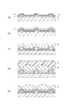
次に、本実施形態の表示装置の製造方法について図2を参照して説明する。図2は、本実施形態の表示装置の各製造工程を示す概要断面図である。なお、陰極14の形成までは周知な製造工程であるため、ここでは説明を省略する。先ず、図2(a)に示すように、トップエミッション型の有機EL素子が複数形成された基板10を用意する。この有機EL素子は、アクティブマトリクス型の画素回路が形成された基板10の上に、層間絶縁膜、平坦化膜を介して、陽極11、隔壁12、有機EL層13、陰極14を形成したものである。
<Manufacturing method of display device>
Next, a method for manufacturing the display device of this embodiment will be described with reference to FIG. FIG. 2 is a schematic cross-sectional view showing each manufacturing process of the display device of this embodiment. Since the steps up to the formation of the
次に、図2(b)に示すように第1の保護層15を表示領域の全域に形成する。第1の保護層15は、外部の空気中の水分や、レンズ部16を構成する樹脂材料が含有する水分が有機EL素子に接触することを遮断するための、言わば封止機能を有する部材である。そのため、第1の保護層15は、光の透過率が高く、防湿性に優れた部材であることが好ましく、窒化シリコン膜、酸化窒化シリコン膜から構成されることが好ましい。
Next, as shown in FIG. 2B, the first
次に、図2(c)に示すように第1の保護層15上に、レンズ部16の前駆体である樹脂16’を表示領域の全域に形成する。また、樹脂16’の膜厚は、エッチング残渣などのゴミを十分にカバーすることが可能であると共に隔壁12に生じる凹凸を平坦化することが可能なように、10μm乃至100μm程度とする。樹脂材料としては水分含有が少ない熱硬化型樹脂、熱可塑性樹脂、光硬化型樹脂を用いることができる。熱硬化型樹脂と光硬化型樹脂を用いた場合、成膜方法としては、スピンコート法、ディスペンス法などを用いることが可能である。また、第1の保護層15上に、膜厚10μm乃至100μm程度の熱可塑性樹脂のフィルムを真空下にて貼りつける方法も用いることができる。具体的な樹脂材料としては、エポキシ樹脂、ブチル樹脂が好適に用いられる。
Next, as illustrated in FIG. 2C, a
次に、図2(d)に示すように、レンズ部16の集光レンズを成形するための型21を用意し、樹脂材料に気泡が混入しないように、型21を樹脂材料に対して押圧する。
Next, as shown in FIG. 2 (d), a
型21は、一般的な金属で形成することができるが、樹脂材料に光硬化型樹脂を用いる場合は、光を透過させる必要があるため石英基板から形成されることが好ましい。また、型21の樹脂材料に対する剥離性を高めるために、型21の表面に、フッ素樹脂などの膜を形成してもよい。
The
樹脂材料に熱硬化型樹脂を用いる場合は、型21における各レンズの凸部の頂点が、対応する画素の中心とほぼ一致した状態で、樹脂材料を約80℃に加熱することにより硬化させる。
When a thermosetting resin is used as the resin material, the resin material is cured by heating to about 80 ° C. in a state where the apex of the convex portion of each lens in the
硬化温度については、一般的な有機EL層13を構成する有機化合物の耐熱温度が100℃程度であるため、80℃程度の硬化温度が好ましい。
Regarding the curing temperature, since the heat resistant temperature of the organic compound constituting the general
次に、図2(e)に示すように、型21を、硬化した樹脂材料から剥がす。
Next, as shown in FIG. 2E, the
これにより、表面に各画素に対応して集光レンズを有するレンズ部16が形成される。ここで、互いに隣接するレンズは滑らかな曲線(連続的な曲線)で繋がる構成とした。この結果、レンズ部16の表面には、段差や急激に傾きが変化する部分が存在しなくなる。
Thereby, the
このような急激な傾きの変化や段差が存在すると、レンズ部16上に第2の保護層を形成する場合に、段差等の角部に原料ガスが供給され難く、膜成長が阻害される。結果として亀裂が入った状態で第2の保護層が形成され、第2の保護層の封止機能が失われてしまう。よって、型21の表面形状は、このような課題を生じないように、かつ所望の集光特性を示すレンズを形成可能なように設計、加工されることが好ましい。
When such a steep inclination change or step exists, when the second protective layer is formed on the
また、レンズ間の凹部の底部の膜厚が薄いとエッチング残渣などのゴミを十分にカバーすることができずピンホール発生の原因となるため、凹部の底部におけるレンズ部16の最小膜厚は、1μm以上とした。また、凹部の底部におけるレンズ部16の最大膜厚は、吸収による光量減衰や隣接画素からの発光光の漏れ込み防止のために50μm以下とした。
In addition, if the film thickness of the bottom part of the recess between the lenses is thin, dust such as etching residue cannot be sufficiently covered, causing pinholes. Therefore, the minimum film thickness of the
なお、図2(c)〜(e)の集光レンズを形成する工程では、型21による直接形成法の説明を行なったが、レンズは、下記i)〜v)のいずれかの方法によっても作製可能である。
i)フォトリソなどによってパターニングされた樹脂層を熱処理し、リフローによって樹脂層をレンズ形状に変形させる方法。
ii)均一の厚さに形成された光硬化型樹脂層を、面内方向に強度分布を持った光で露光し、この樹脂層を現像することによってレンズを形成する方法。
iii)イオンビームあるいは電子ビーム、レーザー等を用いて、均一の厚さに形成された樹脂材料の表面をレンズ形状に加工する方法。
iv)各画素に適量の樹脂を滴下して自己整合的にレンズを形成する方法。
v)有機EL素子が形成された基板とは別個に、レンズが予め形成された樹脂シートを用意し、両者をアライメントした後、貼り合せることによりレンズを形成する方法。
In addition, in the process of forming the condensing lens of FIGS. 2C to 2E, the direct forming method using the
i) A method in which a resin layer patterned by photolithography or the like is heat-treated, and the resin layer is deformed into a lens shape by reflow.
ii) A method of forming a lens by exposing a photocurable resin layer formed to a uniform thickness with light having an intensity distribution in the in-plane direction and developing the resin layer.
iii) A method of processing the surface of a resin material formed in a uniform thickness into a lens shape using an ion beam, electron beam, laser, or the like.
iv) A method of forming a lens in a self-aligning manner by dropping an appropriate amount of resin on each pixel.
v) A method of forming a lens by preparing a resin sheet on which a lens is previously formed separately from the substrate on which the organic EL element is formed, aligning the two, and then bonding them together.
なお、本発明におけるレンズは、半球型でも良いし、蒲鉾型の半円筒型であっても構わない。蒲鉾型の半円筒状である場合には、上下又は左右方向の何れかにおいて特に集光機能を有する。なお、半円筒型の長さ方向の端部は半球型でも良いし、端面が基板に垂直に形成されていても良い。 The lens in the present invention may be a hemispherical type or a saddle type semicylindrical type. In the case of a bowl-shaped semi-cylindrical shape, it has a light condensing function particularly in either the vertical or horizontal direction. Note that the end portion in the length direction of the semi-cylindrical shape may be a hemispherical shape, or the end face may be formed perpendicular to the substrate.
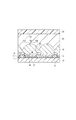
上述したように、レンズ部16は、窒化シリコンなどの無機材料で構成されてもよい。例えば、図3のように示されているような、無機材料のレンズ部16と、その上にレンズ部16の無機材料の屈折率よりも小さい樹脂材料からなる表面に平坦面を有する樹脂層20で構成されていればよい。平坦面は、ガラス板のような透明基板30によって形成されている。平坦面とは、レンズ部16の凹凸を覆って、有機EL素子の発光面とほぼ平行になる面である。この場合も、レンズ部16の表面の少なくとも1点が、式A及び式B、つまり式Cを満たしていれば、本発明の効果が得られる。なお、式A〜Cにおいて、n1はレンズ部16の無機材料の屈折率であり、n2は、その上に形成される樹脂層20の樹脂材料の屈折率である。
As described above, the
また、図3の構成では、樹脂層20から透明基板30に光が入射する際に屈折する。ただし、樹脂層20と透明基板30は平坦面を有するので、透明基板30から空気に出射される光の放射角度は、レンズ部16と樹脂層20との屈折率の関係によって決まり、透明基板30の屈折率には依存しない。また、透明基板30の上に、平坦面を有するものであればどんなものでも積層してもよい。
In the configuration of FIG. 3, the light is refracted when light enters the
レンズ部16を構成する無機材料は、窒化シリコンや酸化窒化シリコンなどが好ましく、その屈折率は1.8乃至2.0である。また、それを覆う樹脂材料としては、上述したレンズ部16に用いられる樹脂材料を用いることができる。
The inorganic material constituting the
無機材料で構成されるレンズ部16は、以下のように形成される。すなわち、第1の保護層15の上に、無機材料の無機膜をCVD法で形成し、この無機膜の上に感光性レジストを塗布し、フォトマスクで露光し現像する。その現像したレジストをマスクにして、所望の表面形状に無機膜をドライエッチングする。こうすることで、無機膜をレンズ部16として成形することができる。
The
さらにレンズ部16の表面にエポキシ樹脂材料等の樹脂材料を塗布し、表面が平坦な面になるよう成形し、樹脂材料を硬化させる。このようにして、レンズ部16とその上の平坦面を有する樹脂層が形成される。
Further, a resin material such as an epoxy resin material is applied to the surface of the
なお、平坦面を有する樹脂層は、その上に平坦なガラス等を貼り合わせて、平坦面を有するようにしてもよい。 Note that the resin layer having a flat surface may have a flat surface by bonding flat glass or the like thereon.
また、レンズ部16と平坦面を有する樹脂層との間に、平坦面を有する樹脂層とは異なる材料の薄膜の樹脂層を形成することもできる。この構成では、その薄膜がレンズ界面での屈折に影響しない程十分薄ければ、式A及び式Bにおけるn1はレンズ部16の屈折率、n2は平坦面を有する樹脂層の屈折率を適用する。
Further, a thin resin layer made of a material different from the resin layer having a flat surface can be formed between the
なお、本発明の表示装置の用途として、高輝度による視認性の向上が重要なモバイル用途、例えばデジタルカメラの背面モニタ、携帯電話用ディスプレイなどが挙げられる。また、同じ輝度でも低消費電力が期待されるので、屋内で使用する用途にも有用である。 Note that applications of the display device of the present invention include mobile applications in which it is important to improve visibility by high luminance, for example, a rear monitor of a digital camera, a display for a mobile phone, and the like. Moreover, since low power consumption is expected even at the same luminance, it is also useful for indoor use.
本発明は、上述した趣旨を逸脱しない限り、以上説明した構成に限られることはなく、種々の応用・変形が可能である。 The present invention is not limited to the above-described configuration without departing from the above-described purpose, and various applications and modifications are possible.
(実施例1)
ガラス基板上に、低温ポリシリコンTFTで画素回路(不図示)を形成し、その上にSiNからなる層間絶縁膜とアクリル樹脂からなる平坦化膜を、この順番で形成して図2(a)に示す基板10を作成した。この基板10上にITO膜/AlNd膜をスパッタリング法にて38nm/100nmの厚さで形成した。続いて、ITO膜/AlNd膜を画素毎にパターニングし、陽極11を形成した。
Example 1
A pixel circuit (not shown) is formed on a glass substrate with a low-temperature polysilicon TFT, and an interlayer insulating film made of SiN and a planarizing film made of acrylic resin are formed on the glass circuit in this order, and FIG. The
この上にアクリル樹脂をスピンコートした。次に、アクリル樹脂をリソグラフィ法により、陽極11が形成された部分に開口(この開口部が画素に相当)が形成されるようにパターニングし隔壁12を形成した。各画素のピッチを30μm、開口による陽極11の露出部の大きさを10μmとした。これをイソプロピルアルコール(IPA)で超音波洗浄し、次いで、煮沸洗浄後乾燥した。さらに、UV/オゾン洗浄してから有機EL層13を真空蒸着により成膜した。
An acrylic resin was spin-coated on this. Next, the
有機EL層13としては、始めに、ホール輸送層をすべての画素に87nmの厚さで成膜した。
As the
次に、シャドーマスクを用いて、赤色発光層、緑色発光層、青色発光層をそれぞれ厚さ30nm、40nm、25nmで画素ごとに成膜した。 Next, using a shadow mask, a red light emitting layer, a green light emitting layer, and a blue light emitting layer were formed for each pixel with a thickness of 30 nm, 40 nm, and 25 nm, respectively.
続いて、すべての画素に共通の電子輸送層を真空蒸着法にて10nmの厚さで形成した。その後、共通の電子注入層を40nmの厚さで形成した。 Subsequently, an electron transport layer common to all the pixels was formed to a thickness of 10 nm by vacuum deposition. Thereafter, a common electron injection layer was formed with a thickness of 40 nm.
次に、上記ホール輸送層から電子注入層までの有機EL層13を成膜した基板を、真空を破ること無しにスパッタ装置に移動し、陰極14として極薄Agおよび透明電極層としてそれぞれ10nm及び50nmの厚さで順に成膜した。透明電極層の材料としては、酸化インジウムと酸化亜鉛の混合物を用いた。
Next, the substrate on which the
次に、図2(b)に示すように、窒化珪素からなる第1の保護層15を、SiH4ガス、N2ガス、H2ガスを用いたプラズマCVD法で成膜した。その後、図2(c)に示すように、露点温度60℃の窒素雰囲気下で、粘度3000mPa・sの熱硬化性の樹脂材料(エポキシ樹脂)を精密描画が可能なディスペンサー(武蔵エンジニアリング社製、製品名SHOT MINI SL)を用いて塗布した。
Next, as shown in FIG. 2B, a first
樹脂材料を熱硬化する前に、図2(d)のように、別途用意した、レンズ部16を成形するための型21を、樹脂材料の表面に押し当てた。押し当てる際、型21に形成してあるアライメントマークと基板に形成してあるアライメントマークをあわせる事により位置決めを行なった。その結果、画素に合わせて集光レンズが形成された。型21は、画素ピッチと同じピッチで凹状に窪みが形成されており、その窪みの表面に離形剤としてテフロン(登録商標)系の樹脂をコートした。窪みの形状、すなわち中央部16aの形状は、曲率半径30μmで形成した。端部16bは、曲率半径100μmで形成した。なお、レンズアレイの高さは4μm程度になった。
Before thermosetting the resin material, a separately
ここで、クリーンルームおよびプロセス装置の環境を考慮して、異物等があっても樹脂材料で平坦化することを目的としているので、レンズ部16の最小膜厚(最薄部における膜厚)は10μmとした。 Here, in consideration of the environment of the clean room and the process apparatus, the objective is to flatten with a resin material even if there is a foreign substance or the like. It was.
上記のように型21を押し当てた状態で、真空環境下で100℃の温度で15分間加熱し、樹脂材料(エポキシ樹脂)を硬化させた。その後、樹脂から型21を離して、図2(e)のように集光レンズを有するレンズ部16を形成した。
With the
このようにして製造した本発明の表示装置の輝度を測定したところ、レンズを形成していない表示装置の輝度と比較すると、真正面から観察した場合には1.5倍程度輝度が向上し、正面から50度傾いた方向から観察した場合は1.1倍程度輝度が向上していた。また、表示装置を水平に近い方向から観察しても、表示装置の画像が確認できた。 When the luminance of the display device of the present invention thus manufactured was measured, the luminance was improved by about 1.5 times when observed from the front, compared with the luminance of the display device without a lens. When observed from a direction inclined by 50 degrees from the angle, the luminance was improved by about 1.1 times. Further, even when the display device was observed from a direction close to the horizontal, the image of the display device could be confirmed.
(実施例2)
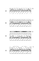
レンズアレイの形成手法として、実施例1とは異なり、図4に示す工程で形成した。なお、第1の保護層15の形成工程までは実施例1と同様であるため説明を省略し、レンズ部16の形成工程から説明を行なう。
(Example 2)
Unlike the first embodiment, the lens array was formed by the process shown in FIG. The process up to the formation of the first
まず、露点温度60℃の窒素雰囲気下で、粘度3000mPa・sの熱硬化性のエポキシ樹脂22を精密描画が可能なディスペンサー(武蔵エンジニアリング社製、製品名SHOT MINI SL)を用いて10μm厚に塗布した(図4(a))。その後、このエポキシ樹脂を真空環境下で100℃の温度で15分間加熱して硬化させた。
First, in a nitrogen atmosphere with a dew point temperature of 60 ° C., a thermosetting
引き続いて、その上に4μm厚でエポキシ樹脂22と同じ材料の樹脂23を塗布し(図4(b))、その上からフォトマスク24で露光した(図4(c))。露光量は集光レンズの形状から換算した2次元の分布を持つように設定した。露光された樹脂を現像することによって、所望の形状の集光レンズが形成された(図4(d))。露光量の面内の制御は、フォトマスク24の透過率を面内で制御することで行なった。その後、樹脂を再度真空環境下で100℃の温度で15分間加熱して硬化させた。この熱処理は、レンズ表面の平滑化も兼ねている。なお、異物等があっても樹脂材料で埋めることを目的としているので、レンズ部16の最小膜厚(最薄部の膜厚)は10μmとした。
Subsequently, a
10 基板
11 陽極
13 有機EL層
14 陰極
15 第1の保護層
16 レンズ部
16a 中央部
16b 端部
16c レンズ
DESCRIPTION OF
Claims (4)
有機EL素子に接して、有機EL素子を保護する保護層と、
前記保護層に接して、有機EL素子の光出射側に配置される、有機EL素子の発光面に対して凸状の集光レンズと、を有し、
前記集光レンズの表面は、以下の式を満たす点を有することを特徴とする表示装置。
sin[θS−Arcsin{(n1/n2)×sin(θS−θ)}]≧1/n2
なお、θは前記有機EL素子から出射されて前記集光レンズの表面に入射されうる光の発光角度、θSは発光角度θで有機EL素子から出射した光が当たる前記集光レンズの表面の傾斜角度、n1は前記集光レンズの屈折率、n2は前記集光レンズの前記有機EL素子とは反対側にある媒質の屈折率である。 An organic EL element;
A protective layer in contact with the organic EL element and protecting the organic EL element;
A condensing lens convex to the light emitting surface of the organic EL element, disposed on the light emitting side of the organic EL element, in contact with the protective layer;
The surface of the said condensing lens has a point which satisfy | fills the following formula | equation, The display apparatus characterized by the above-mentioned.
sin [θ S −Arcsin {(n 1 / n 2 ) × sin (θ S −θ)}] ≧ 1 / n 2
Is the emission angle of light that can be emitted from the organic EL element and incident on the surface of the condenser lens, and θ S is the surface of the condenser lens that is irradiated with the light emitted from the organic EL element at the emission angle θ. The tilt angle, n 1 is the refractive index of the condenser lens, and n 2 is the refractive index of the medium on the opposite side of the condenser lens from the organic EL element.
Priority Applications (3)
| Application Number | Priority Date | Filing Date | Title |
|---|---|---|---|
| JP2011260906A JP2012178332A (en) | 2011-02-04 | 2011-11-29 | Display device |
| US13/364,023 US20120199859A1 (en) | 2011-02-04 | 2012-02-01 | Electroluminescent display apparatus |
| CN2012100236053A CN102629622A (en) | 2011-02-04 | 2012-02-03 | Electroluminescent display apparatus |
Applications Claiming Priority (3)
| Application Number | Priority Date | Filing Date | Title |
|---|---|---|---|
| JP2011022852 | 2011-02-04 | ||
| JP2011022852 | 2011-02-04 | ||
| JP2011260906A JP2012178332A (en) | 2011-02-04 | 2011-11-29 | Display device |
Publications (1)
| Publication Number | Publication Date |
|---|---|
| JP2012178332A true JP2012178332A (en) | 2012-09-13 |
Family
ID=46587843
Family Applications (1)
| Application Number | Title | Priority Date | Filing Date |
|---|---|---|---|
| JP2011260906A Pending JP2012178332A (en) | 2011-02-04 | 2011-11-29 | Display device |
Country Status (3)
| Country | Link |
|---|---|
| US (1) | US20120199859A1 (en) |
| JP (1) | JP2012178332A (en) |
| CN (1) | CN102629622A (en) |
Cited By (2)
| Publication number | Priority date | Publication date | Assignee | Title |
|---|---|---|---|---|
| KR20160032970A (en) * | 2014-09-17 | 2016-03-25 | 엘지디스플레이 주식회사 | Organic light emitting display device and method of manufacturing the same |
| WO2023021365A1 (en) * | 2021-08-19 | 2023-02-23 | 株式会社半導体エネルギー研究所 | Method for manufacturing display device, display device, display module, and electronic apparatus |
Families Citing this family (21)
| Publication number | Priority date | Publication date | Assignee | Title |
|---|---|---|---|---|
| US8324701B2 (en) * | 2010-07-16 | 2012-12-04 | Visera Technologies Company Limited | Image sensors |
| CN105870361B (en) | 2016-05-27 | 2017-12-01 | 京东方科技集团股份有限公司 | Preparation method, optics, display base plate and the display device of optical film |
| CN106129260B (en) * | 2016-06-30 | 2019-03-19 | 京东方科技集团股份有限公司 | A display panel and display device |
| JP2018006212A (en) * | 2016-07-05 | 2018-01-11 | 株式会社ジャパンディスプレイ | Display device |
| KR20180005323A (en) * | 2016-07-05 | 2018-01-16 | 삼성디스플레이 주식회사 | Organic light-emitting display apparatus |
| CN113284933B (en) * | 2016-08-09 | 2025-02-18 | 群创光电股份有限公司 | Organic Light Emitting Diode Display |
| CN107863448B (en) * | 2017-10-24 | 2019-09-06 | 京东方科技集团股份有限公司 | Display screen, manufacturing method thereof, and display device |
| CN114335382B (en) | 2018-12-07 | 2025-03-28 | 京东方科技集团股份有限公司 | Display module and preparation method thereof |
| WO2020162355A1 (en) * | 2019-02-08 | 2020-08-13 | ソニー株式会社 | Light emitting element and display device |
| CN115776825A (en) * | 2019-03-28 | 2023-03-10 | 京东方科技集团股份有限公司 | Silicon-based OLED display assembly and virtual reality display device |
| JP7552588B2 (en) * | 2019-04-26 | 2024-09-18 | ソニーグループ株式会社 | Display devices and electronic devices |
| CN110649084B (en) * | 2019-10-12 | 2022-04-05 | 深圳市华星光电半导体显示技术有限公司 | Display panel and display device |
| WO2021090407A1 (en) * | 2019-11-06 | 2021-05-14 | シャープ株式会社 | Light emitting device |
| CN112542494A (en) * | 2019-12-02 | 2021-03-23 | 创王光电股份有限公司 | Display panel |
| CN111369903A (en) * | 2020-04-08 | 2020-07-03 | 深圳市华星光电半导体显示技术有限公司 | Micro LED display device |
| CN115275062B (en) * | 2020-05-06 | 2025-08-05 | 湖北长江新型显示产业创新中心有限公司 | Display panel, manufacturing method thereof, and display device |
| CN111613734B (en) * | 2020-05-29 | 2023-04-07 | 武汉天马微电子有限公司 | Light extraction layer, manufacturing method thereof and display panel |
| JP7581011B2 (en) * | 2020-10-28 | 2024-11-12 | キヤノン株式会社 | Light-emitting device, display device, imaging device, and electronic device |
| CN112885979A (en) * | 2021-02-01 | 2021-06-01 | 合肥京东方卓印科技有限公司 | Display panel, preparation method thereof and display device |
| KR102941110B1 (en) * | 2021-12-30 | 2026-03-18 | 엘지디스플레이 주식회사 | Viewing Angle Switchable Display Device |
| US20250040319A1 (en) * | 2022-04-20 | 2025-01-30 | Chengdu Boe Optoelectronics Technology Co., Ltd. | Display apparatus, display panel and display baseplate |
Family Cites Families (5)
| Publication number | Priority date | Publication date | Assignee | Title |
|---|---|---|---|---|
| US6679621B2 (en) * | 2002-06-24 | 2004-01-20 | Lumileds Lighting U.S., Llc | Side emitting LED and lens |
| KR100730114B1 (en) * | 2004-04-19 | 2007-06-19 | 삼성에스디아이 주식회사 | Flat Panel Display |
| KR101030537B1 (en) * | 2004-06-30 | 2011-04-21 | 엘지디스플레이 주식회사 | Liquid crystal display and luminance deviation compensation method using the same |
| JP2006251659A (en) * | 2005-03-14 | 2006-09-21 | Fuji Photo Film Co Ltd | Viewing angle expansion film and display device using the viewing angle expansion film |
| TWM332938U (en) * | 2007-08-17 | 2008-05-21 | Lighthouse Technology Co Ltd | Surface mount type light emitting diode package device |
-
2011
- 2011-11-29 JP JP2011260906A patent/JP2012178332A/en active Pending
-
2012
- 2012-02-01 US US13/364,023 patent/US20120199859A1/en not_active Abandoned
- 2012-02-03 CN CN2012100236053A patent/CN102629622A/en active Pending
Cited By (3)
| Publication number | Priority date | Publication date | Assignee | Title |
|---|---|---|---|---|
| KR20160032970A (en) * | 2014-09-17 | 2016-03-25 | 엘지디스플레이 주식회사 | Organic light emitting display device and method of manufacturing the same |
| KR102293473B1 (en) * | 2014-09-17 | 2021-08-24 | 엘지디스플레이 주식회사 | Organic light emitting display device and method of manufacturing the same |
| WO2023021365A1 (en) * | 2021-08-19 | 2023-02-23 | 株式会社半導体エネルギー研究所 | Method for manufacturing display device, display device, display module, and electronic apparatus |
Also Published As
| Publication number | Publication date |
|---|---|
| US20120199859A1 (en) | 2012-08-09 |
| CN102629622A (en) | 2012-08-08 |
Similar Documents
| Publication | Publication Date | Title |
|---|---|---|
| JP5341701B2 (en) | Display device and digital camera | |
| JPWO2011016126A1 (en) | Display device | |
| US20120199859A1 (en) | Electroluminescent display apparatus | |
| US8944616B2 (en) | Display device and image-information processing apparatus equipped with the same | |
| US7531955B2 (en) | OLED device with improved efficiency and robustness | |
| US7602118B2 (en) | OLED device having improved light output | |
| US20070013293A1 (en) | OLED device having spacers | |
| CN104037357B (en) | A kind of organic light-emitting display device and manufacture method thereof | |
| US8344603B2 (en) | Organic electroluminescence display apparatus | |
| US20110241539A1 (en) | Light-Emitting Device and Article | |
| US7825570B2 (en) | LED device having improved contrast | |
| JP2012134128A (en) | Display device | |
| JP2013114772A (en) | Display device | |
| WO2006035811A1 (en) | Organic electroluminescence display device | |
| US8748924B2 (en) | Display apparatus and method for manufacturing the same | |
| CN110148685B (en) | Display panel and method of making the same | |
| JP2013114773A (en) | Display device | |
| CN108963106B (en) | Display panel, manufacturing method thereof and display device | |
| US20210202913A1 (en) | Light extraction apparatus and flexible oled displays | |
| CN117279456A (en) | Display panel, display panel preparation method and display device | |
| CN1937872A (en) | Organic light-emitting device with improved light extraction efficiency | |
| JPWO2014034308A1 (en) | Organic light emitting device and organic light emitting device using organic light emitting device | |
| TW200425792A (en) | Organic electroluminescent device |