JP2012178708A - 発光装置用信号処理回路 - Google Patents
発光装置用信号処理回路 Download PDFInfo
- Publication number
- JP2012178708A JP2012178708A JP2011040458A JP2011040458A JP2012178708A JP 2012178708 A JP2012178708 A JP 2012178708A JP 2011040458 A JP2011040458 A JP 2011040458A JP 2011040458 A JP2011040458 A JP 2011040458A JP 2012178708 A JP2012178708 A JP 2012178708A
- Authority
- JP
- Japan
- Prior art keywords
- signal
- circuit
- light emitting
- emitting device
- signal processing
- Prior art date
- Legal status (The legal status is an assumption and is not a legal conclusion. Google has not performed a legal analysis and makes no representation as to the accuracy of the status listed.)
- Granted
Links
- 239000003990 capacitor Substances 0.000 claims abstract description 56
- 230000010355 oscillation Effects 0.000 claims description 5
- 238000001514 detection method Methods 0.000 claims description 3
- 230000001360 synchronised effect Effects 0.000 claims description 3
- 230000007274 generation of a signal involved in cell-cell signaling Effects 0.000 claims 3
- 230000006866 deterioration Effects 0.000 abstract description 3
- 230000010356 wave oscillation Effects 0.000 description 9
- 230000003321 amplification Effects 0.000 description 4
- 238000003199 nucleic acid amplification method Methods 0.000 description 4
- 238000000034 method Methods 0.000 description 3
- 230000005540 biological transmission Effects 0.000 description 2
- 238000010586 diagram Methods 0.000 description 2
- 238000007599 discharging Methods 0.000 description 2
- 230000000694 effects Effects 0.000 description 2
- 239000011159 matrix material Substances 0.000 description 2
- 230000007423 decrease Effects 0.000 description 1
- 230000003247 decreasing effect Effects 0.000 description 1
Images






Landscapes
- Picture Signal Circuits (AREA)
Abstract
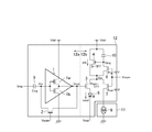
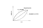
【解決手段】ピクセル回路12は、キャパシタ9、インバータ1、FET2、FET3、FET4、発光ダイオード等による発光素子5、FET6、FET7、キャパシタ9、キャパシタ10で構成される。ドライバー回路11は、定電流源8で構成される。インバータ1から出力されるパルスのパルス幅の変化により発光素子5の輝度レベルを変化させる。キャパシタ9に、輝度信号が保持される。また、三角波の線形部に非線形性を持たせた信号がVsigに入力される。輝度信号と非線形波形信号との差に基づいてインバータ1は、出力パルス幅を決定する。
【選択図】 図1
Description
1a FET
1b FET
2 FET
3 FET
4 キャパシタ
5 FET
6 キャパシタ
7 FET
8 定電流源
9 キャパシタ
10 キャパシタ
11 電源電圧回路
12 ピクセル回路
Claims (10)
- 発光装置に接続された駆動回路に供給されるパルス幅の変化により発光装置の輝度レベルを変化させる発光装置用信号処理回路であって、
入力される輝度信号を保持するとともに前記輝度信号と入力される非線形波形信号とに基づいて出力パルス幅を決定し、前記駆動回路にパルス信号を供給するパルス幅変調回路と、
前記非線形波形信号を生成する非線形波形信号生成回路とを備え、
前記非線形波形信号は三角波の線形部に非線形性を持たせたことを特徴とする発光装置用信号処理回路。 - 前記三角波の線形部に非線形性を持たせたのは、べき乗の非線形性であることを特徴とする請求項1に記載の発光装置用信号処理回路。
- 前記パルス幅変調回路は、前記入力される輝度信号を保持する第1の動作期間と、前記非線形波形信号が入力されてパルス幅が変化したパルス信号を出力する第2の動作期間により作動することを特徴とする請求項1又は請求項2のいずれかに記載の発光装置用信号処理回路。
- 前記非線形波形信号生成回路は、キャパシタを用いた三角波生成回路の前記キャパシタを非線形キャパシタにより構成することを特徴とする請求項1〜請求項3のいずれか1項に記載の発光装置用信号処理回路。
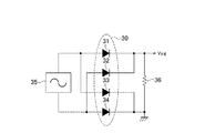
- 前記非線形波形信号生成回路は、正弦波発生回路から出力される正弦波を用いた全波整流回路により構成されていることを特徴とする請求項1〜請求項3のいずれか1項に記載の発光装置用信号処理回路。
- 前記非線形波形信号生成回路は、正弦波発生回路から出力される正弦波を用いた同期検波回路により構成されていることを特徴とする請求項1〜請求項3のいずれか1項に記載の発光装置用信号処理回路。
- 前記正弦波発生回路は、出力される正弦波の周波数及び振幅を適宜設定できることを特徴とする請求項5又は請求項6のいずれかに記載の発光装置用信号処理回路。
- 前記正弦波発生回路は、ウィーンブリッジ発振回路であることを特徴とする請求項7に記載の発光装置用信号処理回路。
- 前記発光装置は発光素子で構成されており、前記発光素子の輝度レベルを変化させることを特徴とする請求項1〜請求項8のいずれか1項に記載の発光装置用信号処理回路。
- 前記発光素子は、発光ダイオードであることを特徴とする請求項9に記載の発光装置用信号処理回路。
Priority Applications (1)
| Application Number | Priority Date | Filing Date | Title |
|---|---|---|---|
| JP2011040458A JP5771807B2 (ja) | 2011-02-25 | 2011-02-25 | 発光装置用信号処理回路 |
Applications Claiming Priority (1)
| Application Number | Priority Date | Filing Date | Title |
|---|---|---|---|
| JP2011040458A JP5771807B2 (ja) | 2011-02-25 | 2011-02-25 | 発光装置用信号処理回路 |
Publications (2)
| Publication Number | Publication Date |
|---|---|
| JP2012178708A true JP2012178708A (ja) | 2012-09-13 |
| JP5771807B2 JP5771807B2 (ja) | 2015-09-02 |
Family
ID=46980271
Family Applications (1)
| Application Number | Title | Priority Date | Filing Date |
|---|---|---|---|
| JP2011040458A Expired - Fee Related JP5771807B2 (ja) | 2011-02-25 | 2011-02-25 | 発光装置用信号処理回路 |
Country Status (1)
| Country | Link |
|---|---|
| JP (1) | JP5771807B2 (ja) |
Cited By (1)
| Publication number | Priority date | Publication date | Assignee | Title |
|---|---|---|---|---|
| CN117595067A (zh) * | 2024-01-18 | 2024-02-23 | 深圳市吉斯迪科技有限公司 | 一种电容储能脉冲激光器恒流电源电路 |
Citations (4)
| Publication number | Priority date | Publication date | Assignee | Title |
|---|---|---|---|---|
| JPH02100944U (ja) * | 1989-01-31 | 1990-08-10 | ||
| JPH11338404A (ja) * | 1998-04-30 | 1999-12-10 | Hewlett Packard Co <Hp> | アナログ駆動回路 |
| JP2006073894A (ja) * | 2004-09-03 | 2006-03-16 | Advanced Telecommunication Research Institute International | 半導体装置 |
| JP2009300592A (ja) * | 2008-06-11 | 2009-12-24 | Hitachi Displays Ltd | 画像表示装置 |
-
2011
- 2011-02-25 JP JP2011040458A patent/JP5771807B2/ja not_active Expired - Fee Related
Patent Citations (4)
| Publication number | Priority date | Publication date | Assignee | Title |
|---|---|---|---|---|
| JPH02100944U (ja) * | 1989-01-31 | 1990-08-10 | ||
| JPH11338404A (ja) * | 1998-04-30 | 1999-12-10 | Hewlett Packard Co <Hp> | アナログ駆動回路 |
| JP2006073894A (ja) * | 2004-09-03 | 2006-03-16 | Advanced Telecommunication Research Institute International | 半導体装置 |
| JP2009300592A (ja) * | 2008-06-11 | 2009-12-24 | Hitachi Displays Ltd | 画像表示装置 |
Cited By (2)
| Publication number | Priority date | Publication date | Assignee | Title |
|---|---|---|---|---|
| CN117595067A (zh) * | 2024-01-18 | 2024-02-23 | 深圳市吉斯迪科技有限公司 | 一种电容储能脉冲激光器恒流电源电路 |
| CN117595067B (zh) * | 2024-01-18 | 2024-04-02 | 深圳市吉斯迪科技有限公司 | 一种电容储能脉冲激光器恒流电源电路 |
Also Published As
| Publication number | Publication date |
|---|---|
| JP5771807B2 (ja) | 2015-09-02 |
Similar Documents
| Publication | Publication Date | Title |
|---|---|---|
| US9424770B2 (en) | Error compensator and organic light emitting display device using the same | |
| US9972246B2 (en) | Pixel and organic light emitting display including the same | |
| KR102276536B1 (ko) | 발광 소자 구동 회로, 표시 장치, 및, a/d 변환 회로 | |
| JP3935891B2 (ja) | ランプ電圧発生装置及びアクティブマトリクス駆動型表示装置 | |
| CN105336292B (zh) | Oled像素补偿电路和oled像素驱动方法 | |
| JP6882591B2 (ja) | Amoledピクセル駆動回路及びピクセル駆動方法 | |
| JP7316776B2 (ja) | 半導体装置 | |
| US9591715B2 (en) | OLED driving compensation circuit and driving method thereof | |
| US20060022305A1 (en) | Active-matrix-driven display device | |
| US11087693B2 (en) | Pixel circuit, method of driving pixel circuit, display panel and display device | |
| US20130063498A1 (en) | Display apparatus | |
| JP5395728B2 (ja) | 発光表示装置の駆動方法 | |
| CN105139807A (zh) | 一种像素驱动电路、显示装置及其驱动方法 | |
| CN110232889B (zh) | 像素驱动电路以及显示面板 | |
| CN108520719B (zh) | 驱动控制电路及方法 | |
| CN106531082A (zh) | 一种像素驱动电路、显示面板、显示设备和像素驱动方法 | |
| CN102654978B (zh) | 反相器电路和显示单元 | |
| US20110032282A1 (en) | Display device and driving method thereof | |
| KR20150107715A (ko) | 표시 장치, 표시 구동 장치, 구동 방법, 및 전자 기기 | |
| CN106652913B (zh) | 一种像素驱动电路、显示面板、显示设备和像素驱动方法 | |
| JP5771807B2 (ja) | 発光装置用信号処理回路 | |
| KR102348665B1 (ko) | 유기발광 표시장치 | |
| CN118015961A (zh) | 像素电路 | |
| JP4817915B2 (ja) | 画像表示装置及びその駆動方法 | |
| JP2005301234A (ja) | 表示装置 |
Legal Events
| Date | Code | Title | Description |
|---|---|---|---|
| A621 | Written request for application examination |
Free format text: JAPANESE INTERMEDIATE CODE: A621 Effective date: 20140128 |
|
| A977 | Report on retrieval |
Free format text: JAPANESE INTERMEDIATE CODE: A971007 Effective date: 20150115 |
|
| A131 | Notification of reasons for refusal |
Free format text: JAPANESE INTERMEDIATE CODE: A131 Effective date: 20150203 |
|
| A521 | Written amendment |
Free format text: JAPANESE INTERMEDIATE CODE: A523 Effective date: 20150326 |
|
| TRDD | Decision of grant or rejection written | ||
| A01 | Written decision to grant a patent or to grant a registration (utility model) |
Free format text: JAPANESE INTERMEDIATE CODE: A01 Effective date: 20150422 |
|
| A61 | First payment of annual fees (during grant procedure) |
Free format text: JAPANESE INTERMEDIATE CODE: A61 Effective date: 20150522 |
|
| R150 | Certificate of patent or registration of utility model |
Ref document number: 5771807 Country of ref document: JP Free format text: JAPANESE INTERMEDIATE CODE: R150 |
|
| LAPS | Cancellation because of no payment of annual fees |