JP2012181585A - Device system and chip - Google Patents
Device system and chip Download PDFInfo
- Publication number
- JP2012181585A JP2012181585A JP2011042446A JP2011042446A JP2012181585A JP 2012181585 A JP2012181585 A JP 2012181585A JP 2011042446 A JP2011042446 A JP 2011042446A JP 2011042446 A JP2011042446 A JP 2011042446A JP 2012181585 A JP2012181585 A JP 2012181585A
- Authority
- JP
- Japan
- Prior art keywords
- repeater
- chip
- request
- response
- external
- Prior art date
- Legal status (The legal status is an assumption and is not a legal conclusion. Google has not performed a legal analysis and makes no representation as to the accuracy of the status listed.)
- Pending
Links
- 230000004044 response Effects 0.000 claims abstract description 121
- 238000004891 communication Methods 0.000 claims abstract description 57
- 230000015654 memory Effects 0.000 claims description 34
- 230000005540 biological transmission Effects 0.000 claims description 27
- 238000006243 chemical reaction Methods 0.000 claims description 21
- 239000007788 liquid Substances 0.000 claims 2
- 238000012546 transfer Methods 0.000 abstract description 10
- 238000000034 method Methods 0.000 abstract description 6
- 230000008569 process Effects 0.000 abstract description 5
- 230000006870 function Effects 0.000 description 18
- 239000000976 ink Substances 0.000 description 13
- 238000012545 processing Methods 0.000 description 12
- 238000010586 diagram Methods 0.000 description 8
- 230000004048 modification Effects 0.000 description 6
- 238000012986 modification Methods 0.000 description 6
- 230000007246 mechanism Effects 0.000 description 5
- 230000032258 transport Effects 0.000 description 2
- 230000009118 appropriate response Effects 0.000 description 1
- 238000010438 heat treatment Methods 0.000 description 1
- 239000004973 liquid crystal related substance Substances 0.000 description 1
- 238000003825 pressing Methods 0.000 description 1
- 238000004886 process control Methods 0.000 description 1
Images



Landscapes
- Multi Processors (AREA)
- Information Transfer Systems (AREA)
Abstract
【課題】拡張性のよいシステムを提供する。
【解決手段】マスター(プロセッサー52a)は送信先のスレーブ(SDRAMコントローラー34)の識別情報S1と自身の識別情報M3とを格納してリクエストを送信し、ルーター57は識別情報S1に基づいてポートP56にリクエストを転送し、チップリンク58,39を介してリクエストを受信したルーター37は識別情報S1に基づいてポートP33にリクエストを転送する。スレーブは識別情報M3を格納してレスポンスを送信し、ルーター37は識別情報M3に基づいてポートP35にレスポンスを転送し、チップリンク39,58を介してレスポンスを受信したルーター57は識別情報M3に基づいてポートP51にレスポンスを転送する。これにより、マスターやスレーブ,各ルーターは、チップ内の通信と同様な処理でチップ31,47間の通信を行なうことができる。
【選択図】図2A system with good expandability is provided.
A master (processor 52a) stores identification information S1 of a destination slave (SDRAM controller 34) and its own identification information M3 and transmits a request, and a router 57 sends a port P56 based on the identification information S1. The router 37 that receives the request via the chip links 58 and 39 transfers the request to the port P33 based on the identification information S1. The slave stores the identification information M3 and transmits a response. The router 37 forwards the response to the port P35 based on the identification information M3. The router 57 that receives the response via the chip links 39 and 58 receives Based on this, the response is transferred to the port P51. As a result, the master, slave, and each router can perform communication between the chips 31 and 47 by the same process as the communication within the chip.
[Selection] Figure 2
Description
本発明は、登録された送信先に対するリクエストを送信するマスターと、該リクエストに対するレスポンスを送信するスレーブと、前記マスターと前記スレーブとにポートを介して接続される内部中継器とが搭載される複数のチップを接続してなるデバイスシステムおよびチップに関する。 The present invention includes a plurality of masters that transmit a request to a registered destination, a slave that transmits a response to the request, and an internal repeater that is connected to the master and the slave via a port. The present invention relates to a device system and a chip formed by connecting the chips.
従来より、複数のプロセッサーと、ルーターと、メモリー通信コントローラーと、ネットワークインターフェースコントローラーとから構成されるネットワークオンチップ(NOC)を複数備えたデバイスシステムが提案されている(例えば、特許文献1参照)。このシステムでは、各プロセッサーがルーターにメモリー通信コントローラーやネットワークインターフェースコントローラーを介して接続され、メモリー通信コントローラーによりチップ内におけるプロセッサーとメモリー間の通信を制御し、ネットワークインターフェースコントローラーによりチップ間におけるプロセッサー相互の通信を制御するものとしている。 Conventionally, a device system including a plurality of network-on-chip (NOC) devices including a plurality of processors, a router, a memory communication controller, and a network interface controller has been proposed (see, for example, Patent Document 1). In this system, each processor is connected to the router via a memory communication controller or network interface controller. The memory communication controller controls communication between the processor and the memory in the chip, and the network interface controller communicates between the processors between the chips. To control.
上述したシステムにおいては、チップ内の通信とチップ間の通信とがそれぞれ異なるコントローラーによって行なわれており、チップの数を増やしてシステムを拡張する際には各コントローラーをそれぞれ追加しなければならず、拡張に対する負担が大きなものとなってしまう。ここで、近年、このような複数のチップを備えるシステムが増加しており、搭載されるチップの数は今後さらに増えることが予想されるため、そのようなシステムの拡張に対する要請が高まることが考えられる。 In the system described above, communication within a chip and communication between chips are performed by different controllers, and each controller must be added when expanding the system by increasing the number of chips. The burden for expansion becomes large. Here, in recent years, the number of systems including a plurality of chips has increased, and the number of chips to be mounted is expected to increase further in the future. It is done.
本発明のデバイスシステムおよびチップは、拡張性のよいシステムを提供することを主目的とする。 The main object of the device system and the chip of the present invention is to provide a system with good expandability.
本発明のデバイスシステムおよびチップは、上述の主目的を達成するために以下の手段を採った。 The device system and the chip of the present invention employ the following means in order to achieve the main object described above.
本発明のデバイスシステムは、
登録された送信先に対するリクエストを送信するマスターと、該リクエストに対するレスポンスを送信するスレーブと、前記マスターと前記スレーブとにポートを介して接続される内部中継器とが搭載される複数のチップを接続してなるデバイスシステムであって、
前記内部中継器に前記ポートを介して接続される第1の外部中継器と第2の外部中継器とを一組として、少なくとも該一組の外部中継器同士の接続により前記各チップが接続され、
前記マスターは、前記送信先として、自身が搭載されるチップ内のスレーブと、自身が搭載されるチップ内の前記第1の外部中継器を介して接続される接続先のチップ内のスレーブとが登録され、前記送信先に選択したスレーブの識別情報と自身の識別情報であるマスターの識別情報とを格納して前記リクエストを生成して送信し、
前記スレーブは、前記リクエスト内の前記マスターの識別情報を格納して前記レスポンスを生成して送信し、
前記内部中継器は、前記ポートに接続される接続先の識別情報と該ポートとの対応関係として、前記マスターの識別情報と該マスターに接続されるポートとの対応と、前記スレーブの識別情報と該スレーブに接続されるポートとの対応と、前記第1の外部中継器を介して接続される接続先のチップ内のスレーブの識別情報と該第1の外部中継器に接続されるポートとの対応と、前記第2の外部中継器を介して接続される接続先のチップ内のマスターの識別情報と該第2の外部中継器に接続されるポートとの対応とをそれぞれ記憶し、前記リクエストを受信すると該リクエスト内の前記スレーブの識別情報と前記対応関係とに基づいて選択したポートから該リクエストを送信し、前記レスポンスを受信すると該レスポンス内の前記マスターの識別情報と前記対応関係とに基づいて選択したポートから該レスポンスを送信し、
前記第1の外部中継器は、前記内部中継器から前記リクエストを受信すると接続先の前記第2の外部中継器に該リクエストを送信し、接続先の前記第2の外部中継器から前記レスポンスを受信すると前記内部中継器に該レスポンスを送信し、
前記第2の外部中継器は、接続先の前記第1の外部中継器から前記リクエストを受信すると該リクエストを前記内部中継器に送信し、前記内部中継器から前記レスポンスを受信すると該レスポンスを接続先の前記第1の外部中継器に送信する
ことを要旨とする。
The device system of the present invention includes:
Connects a plurality of chips mounted with a master that transmits a request to a registered transmission destination, a slave that transmits a response to the request, and an internal repeater that is connected to the master and the slave via a port A device system comprising:
The first external repeater and the second external repeater connected to the internal repeater via the port as a set, and each chip is connected by connecting at least the set of external repeaters. ,
The master includes, as the transmission destination, a slave in a chip on which the master is mounted and a slave in a connection destination chip connected via the first external repeater in the chip on which the master is mounted. Registered and stored the identification information of the slave selected as the transmission destination and the identification information of the master that is the identification information of itself to generate and transmit the request,
The slave stores the identification information of the master in the request and generates and transmits the response,
The internal repeater has a correspondence relationship between identification information of a connection destination connected to the port and the port, correspondence between the identification information of the master and a port connected to the master, identification information of the slave, Correspondence between a port connected to the slave, identification information of a slave in a connection destination chip connected via the first external repeater, and a port connected to the first external repeater Storing the correspondence and the correspondence between the identification information of the master in the connection destination chip connected via the second external repeater and the port connected to the second external repeater; Is received from the port selected based on the identification information of the slave in the request and the corresponding relationship, and when the response is received, the identification of the master in the response is received. Transmitted the response from the port selected on the basis of the information and the correspondence relation,
When the first external repeater receives the request from the internal repeater, the first external repeater transmits the request to the second external repeater to be connected, and receives the response from the second external repeater to be connected. When receiving, send the response to the internal repeater,
The second external repeater transmits the request to the internal repeater when receiving the request from the first external repeater to which it is connected, and connects the response when receiving the response from the internal repeater The gist is to transmit to the first external repeater.
この本発明のデバイスシステムでは、内部中継器は、ポートに接続される接続先の識別情報とポートとの対応関係として、マスターの識別情報とマスターに接続されるポートとの対応と、スレーブの識別情報とスレーブに接続されるポートとの対応と、第1の外部中継器を介して接続される接続先のチップ内のスレーブの識別情報と第1の外部中継器に接続されるポートとの対応と、第2の外部中継器を介して接続される接続先のチップ内のマスターの識別情報と第2の外部中継器に接続されるポートとの対応とをそれぞれ記憶し、リクエストを受信するとマスターにより格納されたリクエスト内のスレーブの識別情報と対応関係とに基づいて選択したポートからリクエストを送信し、レスポンスを受信するとスレーブにより格納されたレスポンス内のマスターの識別情報と対応関係とに基づいて選択したポートからレスポンスを送信する。また、第1の外部中継器は、内部中継器からリクエストを受信すると接続先の第2の外部中継器にリクエストを送信し、接続先の第2の外部中継器からレスポンスを受信すると内部中継器にレスポンスを送信し、第2の外部中継器は、接続先の第1の外部中継器からリクエストを受信するとリクエストを内部中継器に送信し、内部中継器からレスポンスを受信するとレスポンスを接続先の第1の外部中継器に送信する。これにより、マスターやスレーブ、内部中継器における各処理をチップ内での通信とチップ間での通信とにおいて同様なものとすることができる。このため、チップ内の通信とチップ間の通信とを異なるコントローラーなどを用いて制御するものなどに比して、チップの数が増加した場合の対応が容易となるから、拡張性のよいシステムを提供することができる。 In the device system of the present invention, the internal repeater, as the correspondence relationship between the identification information of the connection destination connected to the port and the port, the correspondence between the identification information of the master and the port connected to the master, and the identification of the slave Correspondence between information and port connected to slave, correspondence between identification information of slave in connection destination chip connected via first external repeater and port connected to first external repeater And the correspondence between the identification information of the master in the connection destination chip connected via the second external repeater and the port connected to the second external repeater, and the master when receiving the request When a request is sent from the port selected based on the slave identification information and the correspondence in the request stored by Sending a response from the selected port on the basis of the master of the identification information in Nsu and to the correspondence relationship. When the first external repeater receives a request from the internal repeater, the first external repeater transmits a request to the connected second external repeater, and when receiving a response from the connected second external repeater, the internal repeater The second external repeater transmits a request to the internal repeater when receiving a request from the first external repeater connected to the second external repeater, and receives a response from the internal repeater when receiving a response from the internal repeater. Transmit to the first external repeater. Thereby, each process in a master, a slave, and an internal repeater can be made the same in communication within a chip | tip and communication between chips | tips. For this reason, it is easier to deal with an increase in the number of chips compared to a system that uses different controllers to control communication within the chip and communication between chips. Can be provided.
また、バスクロックの周波数が異なる前記チップを接続してなる本発明のデバイスシステムにおいて、前記第1の外部中継器は、接続先の前記第2の外部中継器から前記レスポンスを受信すると自身が搭載されるチップのバスクロックの周波数に合わせて前記内部中継器に該レスポンスを送信し、前記第2の外部中継器は、接続先の前記第1の外部中継器から前記リクエストを受信すると自身が搭載されるチップのバスクロックの周波数に合わせて前記内部中継器に該リクエストを送信するものとすることもできる。こうすれば、バスクロックの周波数が異なるチップを接続する場合であっても、チップ内での通信とチップ間での通信とを同様なものとして対応することができ、容易にチップ間の通信を拡張することができる。 Further, in the device system of the present invention in which the chips having different bus clock frequencies are connected, the first external repeater is mounted when receiving the response from the second external repeater connected to The response is transmitted to the internal repeater according to the frequency of the bus clock of the chip to be mounted, and the second external repeater is mounted when it receives the request from the first external repeater to which it is connected The request may be transmitted to the internal repeater in accordance with the frequency of the bus clock of the chip to be processed. In this way, even when chips with different bus clock frequencies are connected, communication within the chip and communication between chips can be handled in the same way, and communication between chips can be easily performed. Can be extended.
そして、前記チップ内の通信をパラレル形式のデータで行なう本発明のデバイスシステムにおいて、前記第1の外部中継器は、前記内部中継器から前記リクエストを受信すると自身が搭載されるチップのバスクロックの周波数よりも高い周波数に基づいてパラレル形式からシリアル形式に変換するパラレルシリアル変換を施して接続先の前記第2の外部中継器に該リクエストを送信し、接続先の前記第2の外部中継器から前記レスポンスを受信すると自身が搭載されるチップのバスクロックの周波数に基づいてシリアル形式からパラレル形式に変換するシリアルパラレル変換を施して前記内部中継器に該レスポンスを送信し、前記第2の外部中継器は、接続先の前記第1の外部中継器から前記リクエストを受信すると自身が搭載されるチップのバスクロックの周波数に基づいてシリアル形式からパラレル形式に変換するシリアルパラレル変換を施して該リクエストを前記内部中継器に送信し、前記内部中継器から前記レスポンスを受信すると自身が搭載されるチップのバスクロックの周波数よりも高い周波数に基づいてパラレル形式からシリアル形式に変換するパラレルシリアル変換を施して該レスポンスを接続先の前記第1の外部中継器に送信するものとすることもできる。こうすれば、チップ間におけるリクエストやレスポンスの送信を効率よく行なうことができる。 In the device system of the present invention in which communication within the chip is performed using parallel format data, the first external repeater receives the request from the internal repeater, and the bus clock of the chip on which the first external repeater is mounted. A parallel serial conversion for converting from a parallel format to a serial format based on a frequency higher than the frequency is performed, and the request is transmitted to the second external repeater at the connection destination. From the second external repeater at the connection destination, When the response is received, the response is transmitted to the internal repeater by performing serial / parallel conversion for converting the serial format to the parallel format based on the bus clock frequency of the chip on which the response is mounted, and the second external relay The chip mounted on itself when receiving the request from the first external repeater connected to A bus of a chip on which the request is sent to the internal repeater after receiving the response from the internal repeater after receiving the response from the internal repeater by performing serial / parallel conversion based on the frequency of the bus clock. It is also possible to perform parallel-serial conversion for converting from a parallel format to a serial format based on a frequency higher than the frequency of the clock, and transmit the response to the first external repeater that is the connection destination. In this way, requests and responses can be efficiently transmitted between chips.
さらに、本発明のデバイスシステムにおいて、媒体に画像を形成する画像形成装置に搭載されてなるものとすることもできる。液滴を吐出する複数のノズルが形成された吐出ヘッドを備え、該ノズルから液滴を吐出することにより前記媒体に画像を形成する画像形成装置に搭載されるこの態様の本発明のデバイスシステムにおいて、前記マスターとして前記複数のノズルからの液滴の吐出を制御するプロセッサーを備えると共に前記スレーブとして前記液滴の吐出に関するデータを記憶するメモリーへの該データの読み書きを制御するメモリーコントローラーを備えるものとすることもできる。ここで、このような吐出ヘッドには数百個から数千個のノズルが形成されており、将来的には数万個となることも予想されている。このため、プロセッサーの数も膨大なものとなり、システムの拡張の必要性が高まることが考えられるから、本発明を適用する意義が高い。さらに、この態様の本発明の画像形成装置において、前記プロセッサーとして前記複数のノズルを個々のノズル毎に制御するプロセッサーを該ノズルと同じ数だけ備えるものとすることもできるし、前記プロセッサーとして前記複数のノズルをいくつかのノズル毎にまとめて制御する複数のプロセッサーを備えるものとすることもできる。 Furthermore, the device system of the present invention may be mounted on an image forming apparatus that forms an image on a medium. In the device system of this aspect of the present invention, the device system includes an ejection head in which a plurality of nozzles for ejecting droplets are formed, and is mounted on an image forming apparatus that forms an image on the medium by ejecting droplets from the nozzles. A processor for controlling ejection of droplets from the plurality of nozzles as the master, and a memory controller for controlling reading and writing of the data to a memory for storing data relating to ejection of the droplets as the slave; You can also Here, hundreds to thousands of nozzles are formed in such an ejection head, and it is expected that the number will become tens of thousands in the future. For this reason, the number of processors becomes enormous, and it is considered that the necessity for system expansion is increased. Therefore, the significance of applying the present invention is high. Furthermore, in the image forming apparatus of the present invention of this aspect, the processor may be provided with the same number of processors that control the plurality of nozzles for each nozzle as the processor. It is also possible to provide a plurality of processors that collectively control the nozzles of several nozzles.
本発明のチップは、
登録された送信先に対するリクエストを送信するマスターと、該リクエストに対するレスポンスを送信するスレーブと、前記マスターと前記スレーブとにポートを介して接続される内部中継器とが搭載されるチップであって、
前記内部中継器に前記ポートを介して接続される第1の外部中継器と第2の外部中継器とを一組として、少なくとも該一組の外部中継器同士の接続により他のチップと接続され、
前記マスターは、前記送信先として、前記チップ内のスレーブと、前記第1の外部中継器を介して接続される接続先のチップ内のスレーブとが登録され、前記送信先に選択したスレーブの識別情報と自身の識別情報であるマスターの識別情報とを格納して前記リクエストを生成して送信し、
前記スレーブは、前記リクエスト内の前記マスターの識別情報を格納して前記レスポンスを生成して送信し、
前記内部中継器は、前記ポートに接続される接続先の識別情報と該ポートとの対応関係として、前記マスターの識別情報と該マスターに接続されるポートとの対応と、前記スレーブの識別情報と該スレーブに接続されるポートとの対応と、前記第1の外部中継器を介して接続される接続先のチップ内のスレーブの識別情報と該第1の外部中継器に接続されるポートとの対応と、前記第2の外部中継器を介して接続される接続先のチップ内のマスターの識別情報と該第2の外部中継器に接続されるポートとの対応とをそれぞれ記憶し、前記リクエストを受信すると該リクエスト内の前記スレーブの識別情報と前記対応関係とに基づいて選択したポートから該リクエストを送信し、前記レスポンスを受信すると該レスポンス内の前記マスターの識別情報と前記対応関係とに基づいて選択したポートから該レスポンスを送信し、
前記第1の外部中継器は、前記内部中継器から前記リクエストを受信すると接続先のチップ内の前記第2の外部中継器に該リクエストを送信し、接続先のチップ内の前記第2の外部中継器から前記レスポンスを受信すると前記内部中継器に該レスポンスを送信し、
前記第2の外部中継器は、接続先のチップ内の前記第1の外部中継器から前記リクエストを受信すると該リクエストを前記内部中継器に送信し、前記内部中継器から前記レスポンスを受信すると該レスポンスを接続先のチップ内の前記第1の外部中継器に送信する
ことを要旨とする。
The chip of the present invention is
A chip on which a master that transmits a request for a registered transmission destination, a slave that transmits a response to the request, and an internal repeater connected to the master and the slave via a port,
A set of the first external repeater and the second external repeater connected to the internal repeater via the port is connected to another chip by connecting at least the set of external repeaters. ,
The master registers the slave in the chip and the slave in the connection destination chip connected via the first external repeater as the transmission destination, and identifies the slave selected as the transmission destination. Storing the information and the identification information of the master that is its own identification information, generating and sending the request,
The slave stores the identification information of the master in the request and generates and transmits the response,
The internal repeater has a correspondence relationship between identification information of a connection destination connected to the port and the port, correspondence between the identification information of the master and a port connected to the master, identification information of the slave, Correspondence between a port connected to the slave, identification information of a slave in a connection destination chip connected via the first external repeater, and a port connected to the first external repeater Storing the correspondence and the correspondence between the identification information of the master in the connection destination chip connected via the second external repeater and the port connected to the second external repeater; Is received from the port selected based on the identification information of the slave in the request and the corresponding relationship, and when the response is received, the identification of the master in the response is received. Transmitted the response from the port selected on the basis of the information and the correspondence relation,
When the first external repeater receives the request from the internal repeater, the first external repeater transmits the request to the second external repeater in the connection destination chip, and the second external repeater in the connection destination chip. When the response is received from the repeater, the response is transmitted to the internal repeater,
The second external repeater transmits the request to the internal repeater when receiving the request from the first external repeater in the connected chip, and receives the response from the internal repeater when the request is received. The gist is to transmit the response to the first external repeater in the chip of the connection destination.
この本発明のチップでは、内部中継器は、ポートに接続される接続先の識別情報とポートとの対応関係として、マスターの識別情報とマスターに接続されるポートとの対応と、スレーブの識別情報とスレーブに接続されるポートとの対応と、第1の外部中継器を介して接続される接続先のチップ内のスレーブの識別情報と第1の外部中継器に接続されるポートとの対応と、第2の外部中継器を介して接続される接続先のチップ内のマスターの識別情報と第2の外部中継器に接続されるポートとの対応とをそれぞれ記憶し、リクエストを受信するとマスターにより格納されたリクエスト内のスレーブの識別情報と対応関係とに基づいて選択したポートからリクエストを送信し、レスポンスを受信するとスレーブにより格納されたレスポンス内のマスターの識別情報と対応関係とに基づいて選択したポートからレスポンスを送信する。また、第1の外部中継器は、内部中継器からリクエストを受信すると接続先の第2の外部中継器にリクエストを送信し、接続先の第2の外部中継器からレスポンスを受信すると内部中継器にレスポンスを送信し、第2の外部中継器は、接続先の第1の外部中継器からリクエストを受信するとリクエストを内部中継器に送信し、内部中継器からレスポンスを受信するとレスポンスを接続先の第1の外部中継器に送信する。これにより、マスターやスレーブ、内部中継器における各処理をチップ内での通信とチップ間での通信とにおいて同様なものとすることができる。このため、チップ内の通信とチップ間の通信とを異なるコントローラーなどを用いて行なうものなどに比して、チップの数が増加しても容易にチップ間の通信を拡張することができるから、このチップを複数備えるものとすれば、拡張性のよいシステムを提供することができる。 In the chip according to the present invention, the internal repeater has a correspondence between the identification information of the connection destination connected to the port and the port, the correspondence between the identification information of the master and the port connected to the master, and the identification information of the slave. And the port connected to the slave, the correspondence between the identification information of the slave in the connection destination chip connected via the first external repeater and the port connected to the first external repeater , Storing the identification information of the master in the connection destination chip connected via the second external repeater and the correspondence between the port connected to the second external repeater and receiving the request by the master When a request is sent from the selected port based on the identification information and correspondence of the slave in the stored request and a response is received, the request Sending a response from the selected port on the basis of the star identification information and correspondence. When the first external repeater receives a request from the internal repeater, the first external repeater transmits a request to the connected second external repeater, and when receiving a response from the connected second external repeater, the internal repeater The second external repeater transmits a request to the internal repeater when receiving a request from the first external repeater connected to the second external repeater, and receives a response from the internal repeater when receiving a response from the internal repeater. Transmit to the first external repeater. Thereby, each process in a master, a slave, and an internal repeater can be made the same in communication within a chip | tip and communication between chips | tips. For this reason, communication between chips can be easily expanded even if the number of chips is increased, compared to the case where communication between chips and communication between chips are performed using different controllers. If a plurality of chips are provided, a system with good expandability can be provided.
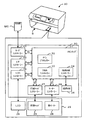
次に、本発明の実施の形態を図面を用いて説明する。図1は、プリンター20の構成の概略を示す構成図であり、図2は、メインチップ31と印刷ヘッドコントローラー47との構成を示す構成図である。本実施形態のプリンター20は、図1に示すように、インクを吐出することにより用紙Sに印刷を行なう周知のインクジェット方式のプリンター機構22と、液晶ディスプレイとしてのLCD28と、装置各部の制御や装置各部の機能を実現するための各種処理などを行なうための処理制御部30とを備える。
Next, embodiments of the present invention will be described with reference to the drawings. FIG. 1 is a configuration diagram showing an outline of the configuration of the
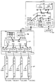
プリンター機構22は、図2に示すように、シアン(C),マゼンタ(M),イエロー(Y),ブラック(K)のCMYKのインクを吐出するノズル24C,24M,24Y,24Kが各色毎に複数個配置された4列のノズル列25C,25M,25Y,25Kが形成された印刷ヘッド23と、印刷ヘッド23を搭載する図示しないキャリッジを主走査方向に駆動するモーターや主走査方向に直交する副走査方向に用紙Sを搬送する図示しない搬送ローラーを駆動するモーターなどの各モーター26とを備える。ここで、印刷ヘッド23は、本実施形態では、圧電素子に電圧を印加してこの圧電素子を変形させることによりインクを加圧してインク滴を吐出する方式を採用するものとした。なお、発熱抵抗体(例えばヒーターなど)に電圧を印加してインクを加熱することにより発生した気泡によりインクを加圧してインク滴を吐出する方式を採用するものとしてもよい。また、ノズル24C,24M,24Y,24Kをノズル24と総称し、ノズル列25C,25M,25Y,25Kをノズル列25と総称する。なお、各ノズル24からのインクの吐出により形成されるドットの大きさは、ノズル24の圧電素子に印可する電圧の波形を変化させることにより、複数段階(例えば、大中小の3段階)に調整可能となっている。
As shown in FIG. 2, the
処理制御部30は、プリンター20の主制御を司るメインプロセッサー32やこのメインプロセッサー32を介さずに各種コントローラーとワークメモリーとの間のデータのやり取りを制御するダイレクトメモリーアクセス(DMA)コントローラー33,ワークメモリーとしてのSDRAM35へのデータの読み書きを制御するSDRAMコントローラー34とが搭載されるメインチップ31と、各種コントローラー41〜49と、各種データなどを記憶した図示しないROMとを備える。なお、以下の説明では、メインチップ31に対して各種コントローラー41〜49をサブチップと称することがあり、チップ内とはメインチップ31内や各種コントローラー41〜49内を意味し、チップ間とは各種コントローラー41〜49のいずれかとメインチップ31との間を意味する。
The
また、処理制御部30は、各種コントローラー41〜49として、写真画像などの画像データが保存されたメモリーカードMCとデータのやり取りを行なうカードコントローラー41と、例えばUSB規格やIEEE1394規格などの所定規格に準拠して図示しない外部機器との通信を行なうI/Fコントローラー43と、LCD28への画像の表示を制御するLCDコントローラー45と、プリンター機構22の印刷ヘッド23を制御する印刷ヘッドコントローラー47と、プリンター機構22の各モーター26を制御するモーターコントローラー49とを備え、これらは、後述するチップリンク接続(図中CL)によりメインチップ31と通信可能に接続されている。一方、メインプロセッサー32は、各種コントローラー41〜49を介して処理に必要なデータを入力したり、各種コントローラー41〜49に各種指令を出力したりする、また、メインプロセッサー32は、カードコントローラー41を介してメモリーカードMCから入力された画像データやI/Fコントローラー43を介して外部機器から入力された画像データに対し、表示用の画像処理を施して生成した表示データや印刷用の画像処理を施して生成した印刷データをSDRAMコントローラー34を介してSDRAM35に保存する。なお、印刷データとしては、ノズル24の圧電素子に印加する電圧の波形を変化させるための駆動データが各ノズル24毎のインク吐出データとして生成されてSDRAM35に保存される。また、DMAコントローラー33の制御により各コントローラー41〜49はメインプロセッサー32を介さずにSDRAM35(SDRAMコントローラー34)と通信が可能となっており、例えば、カードコントローラー41はメモリーカードMCから入力した画像データをSDRAM35に保存したり、LCDコントローラー45はSDRAM35に保存された表示データを取得してLCD28に画像を表示したり、印刷ヘッドコントローラー47はSDRAM35に保存された印刷データ(インク吐出データ)を取得して印刷ヘッド23の各ノズル24からのインクの吐出を制御したりする。
In addition, the
メインチップ31は、上述したメインプロセッサー32やDMAコントローラー33,SDRAMコントローラー34以外に、図2に示すように、キャッシュメモリーとしてのSRAM36aへのデータの読み書きを制御するSRAMコントローラー36と、チップ内の通信を中継するルーター37と、各種コントローラー41〜49(印刷ヘッドコントローラー47を図示)とのチップ間の通信を中継するチップリンク39とを備える。
In addition to the above-described
メインプロセッサー32やDMAコントローラー33は、SDRAM35やSRAM36aなどのメモリーにリードやライトなどのリクエストを出力するマスターとして機能し、識別情報M1,M2が定められている。また、SDRAMコントローラー34やSRAMコントローラー36は、マスターからのリクエストに対するレスポンスを出力するスレーブとして機能し、識別情報S1,S2が定められている。そして、メインプロセッサー32やDMAコントローラー33には、リクエストの送信先としてSDRAMコントローラー34(識別情報S1)やSRAMコントローラー36(識別情報S2)が登録されている。また、メインプロセッサー32やDMAコントローラー33は、送信元を示すSID(SourceID)として識別情報M1あるいは識別情報M2を格納すると共に送信先を示すアドレス情報として送信先に選択したスレーブの識別情報S1や識別情報S2を格納し、リードやライトの種別などの情報も含めてリクエストを生成して送信する。なお、アドレス情報には、スレーブデバイスがメモリーにアクセスするためのアクセス情報なども含まれる。また、SDRAMコントローラー34やSRAMコントローラー36は、アドレス情報に基づいてメモリーにアクセスして必要なデータを読み出すと共にリクエスト内から読み出したSIDを格納してレスポンスを生成して送信する。なお、本実施形態では、これらのリクエストやレスポンスは、送信側が有効に送信できるタイミングであることを示すValid信号や受信側の受信準備が整ったことを示すReady信号などの制御信号により送受信のタイミングが制御されながら、チップ内をパラレルデータとして中継されるものとした。
The
ルーター37は、複数の接続用のポートPを備えており、それらの各ポートPのうち、ポートP31にメインプロセッサー32が接続され、ポートP32にDMAコントローラー33が接続され、ポートP33にSDRAMコントローラー34が接続され、ポートP34にSRAMコントローラー36が接続され、ポートP35にチップリンク39が接続されている。また、このルーター37は、各ポートP31〜P35と接続先の識別情報とを対応付けた対応関係を登録している。具体的には、ポートP31とメインプロセッサー32の識別情報M1とを対応付け、ポートP32とDMAコントローラー33の識別情報M2とを対応付け、ポートP33とSDRAMコントローラー34の識別情報S1とを対応付け、ポートP34とSRAMコントローラー36の識別情報S2とを対応付けて、登録している。また、ポートP35には、チップリンク接続先の印刷ヘッドコントローラー47が備える後述するプロセッサー52a,52b,52c,52dの識別情報M3,M4,M5,M6を、接続先の識別情報として対応付けて登録するものとした。なお、図中の識別番号は、各ポートPに対応付けて登録されている識別番号を示す(以下同じ)。
The
各コントローラー41〜49のうち印刷ヘッドコントローラー47は、図2に示すように、ノズル列25C,25M,25Y,25Kを列毎に個別に制御するプロセッサー52a,52b,52c,52dと、キャッシュメモリーとしてのSRAM56aへのデータの読み書きを制御するSRAMコントローラー56と、メインチップ31との通信を中継するチップリンク58とを備える。ここで、プロセッサー52a,52b,52c,52dは、SRAM56aなどのメモリーにリクエストを出力するマスターとして機能し、メインチップ31のマスターとは異なる識別情報M3,M4,M5,M6が定められている。また、SRAMコントローラー56は、リクエストに対するレスポンスを出力するスレーブとして機能し、メインチップ31のスレーブとは異なる識別情報S3が定められている。また、プロセッサー52a,52b,52c,52dには、リクエストの送信先としてSRAMコントローラー56(識別情報S3)の他、メインチップ31のSDRAMコントローラー34(識別情報S1)やSRAMコントローラー36(識別情報S2)が登録されている。なお、印刷ヘッドコントローラー47におけるリクエストやレスポンスの生成などは、上述したメインチップ31と同様である。
As shown in FIG. 2, the
ルーター57は、複数の接続用のポートPを備えており、それらの各ポートPのうち、ポートP51にプロセッサー52aが接続され、ポートP52にプロセッサー52bが接続され、ポートP53にプロセッサー52cが接続され、ポートP54にプロセッサー52dが接続され、ポートP55にSRAMコントローラー56が接続され、ポートP56にチップリンク58が接続されている。また、このルーター57は、各ポートP51〜P56と接続先の識別情報とを対応付けた対応関係を登録している。具体的には、ポートP51とプロセッサー52aの識別情報M3とを対応付け、ポートP52とプロセッサー52bの識別情報M4とを対応付け、ポートP53とプロセッサー52cの識別情報M5とを対応付け、ポートP54とプロセッサー52dの識別情報M6とを対応付け、ポートP55とSRAMコントローラー56の識別情報S3とを対応付けて、登録している。また、ポートP56には、チップリンク接続先のメインチップ31のSDRAMコントローラー34の識別情報S1やSRAMコントローラー36の識別情報S2を、接続先の識別情報として対応付けて登録するものとした。
The
ここで、チップリンク接続について、チップリンク39とチップリンク58との接続を例として説明する。図3は、チップリンク接続の概要を示す説明図である。図示するように、チップリンク39は、トランスミッター(Tx)39aと、レシーバー(Rx)39bとを備え、チップリンク58は、レシーバー39bに接続されたトランスミッター(Tx)58aと、トランスミッター(Tx)39aに接続されたレシーバー(Rx)58bとを備える。トランスミッター58aは、ルーター57から転送されるパラレルデータであるリクエストをシリアルデータに変換するパラレル−シリアル変換を行なってレシーバー39bに送信する。このとき、トランスミッター58aは、チップ内のバスクロックを所定数倍(数十倍や百倍など)の周波数とする図示しないPLL(Phase Locked Loop)回路からのクロック信号に基づいて、シリアルデータに変換する。また、トランスミッター58aは、リクエストのデータと共にシリアルデータの先頭を示すHeader信号や上述したReady信号やValid信号などの制御信号をレシーバー39bに送信する。そして、レシーバー39bは、トランスミッター58aから送信されるシリアルデータであるリクエストを受信したときには、チップ内のバスクロックに基づいて、パラレルデータに変換するシリアル−パラレル変換を行なって、リクエストのデータと共に送信された制御信号を用いた送受信の制御を伴って、ルーター37に送信する。なお、本実施形態では、メインチップ31のバスクロックの周波数と印刷ヘッドコントローラー47のバスクロックの周波数とは異なるものとした。一方、トランスミッター39aは、ルーター37から転送されるパラレルデータであるレスポンスを受信したときには、チップ内のバスクロックを所定数倍(数十倍や百倍など)の周波数とする図示しないPLL回路からのクロック信号に基づいて、シリアルデータに変換する。また、トランスミッター39aは、レスポンスのデータと共にシリアルデータの先頭を示すHeader信号や上述したReady信号やValid信号などの制御信号をレシーバー58bに送信する。そして、レシーバー58bは、トランスミッター39aから送信されるシリアルデータであるレスポンスを受信したときには、チップ内のバスクロックに基づいて、パラレルデータに変換するシリアル−パラレル変換を行なって、レスポンスのデータと共に送信された制御信号を用いた送受信の制御を伴って、ルーター57に送信する。このように、本実施形態では、印刷ヘッドコントローラー47からメインチップ31にリクエストが送信されたりメインチップ31から印刷ヘッドコントローラー47にレスポンスが送信されたりするものであり、チップリンク58がリクエストを送信するリクエスター(Requester)として機能しチップリンク39がレスポンスを送信するレスポンダー(Responder)として機能するものといえる。
Here, the chip link connection will be described by taking the connection between the
次に、こうして構成された本実施形態のプリンター20における動作、特にチップ内の通信とチップ間の通信とにおける各動作について説明する。まず、チップ内の通信として、印刷ヘッドコントローラー47内のプロセッサー52aとSRAMコントローラー56との通信について説明する。まず、プロセッサー52aは、SRAMコントローラー56の識別情報S3をアドレス情報として格納すると共に自身の識別情報M3をSIDとして格納してリクエストを生成し、生成したリクエストをルーター57に送信する。このリクエストを受信したルーター57は、リクエスト内のアドレス情報から識別情報S3を読み出して上述した対応関係から識別情報S3に対応付けられたポートPとしてポートP55を選択し、選択したポートP55からリクエストを転送する。このリクエストを受信したSRAMコントローラー56は、必要なデータをSRAM56aから読み出すと共にリクエスト内のSIDなどの必要な情報を格納してレスポンスを生成し、生成したレスポンスをルーター57に送信する。このレスポンスを受信したルーター57は、レスポンス内のSIDから識別情報M3を読み出して上述した対応関係から識別情報M3に対応付けられたポートPとしてポートP51を選択し、選択したポートP51からレスポンスを転送して、一連の処理が終了する。このようにして、チップ内の通信が行なわれて、レスポンスがプロセッサー52aに送信されることになる。なお、他のプロセッサー52b,52c,52dとSRAMコントローラー56との通信や他のチップ内の通信も同様に行なわれる。
Next, operations in the
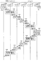
次に、チップ間の通信として、印刷ヘッドコントローラー47とメインチップ31との通信について説明する。ここでは、印刷ヘッドコントローラー47のプロセッサー52aとメインチップ31のSDRAMコントローラー34との通信を例として説明する。図4は、チップ間の通信の一例を示すトランザクションチャートである。なお、このような通信は、例えば、印刷ヘッドコントローラー47からメインチップ31のSDARMコントローラー34に格納された印刷データ(インク吐出データ)を取得する場合などに行なわれる。
Next, communication between the
まず、プロセッサー52aは、登録された送信先の中から選択したSDRAMコントローラー34の識別情報S1をアドレス情報として格納すると共に自身の識別情報M3をSIDとして格納してリクエストを生成し(ステップS100)、生成したリクエストをルーター57に送信する(ステップS110)。このリクエストを受信したルーター57は、リクエスト内のアドレス情報から識別情報S1を読み出して上述した対応関係から識別情報S1に対応付けられたポートPとしてポートP56を選択し(ステップ120)、選択したポートP56からリクエストを転送する(ステップS130)。このようなポートPの選択やレスポンスの転送は、チップ内の通信における処理と同様に行なわれる。上述したように、ポートP56には、識別情報S1,S2を対応付けて登録すると共にチップリンク58が接続されているから、リクエストはチップリンク58に転送されることになる。そして、チップリンク58は、リクエストが転送されると、チップ内(印刷ヘッドコントローラー47内)のバスクロックを所定数倍の周波数としたクロック信号に基づいてトランスミッター58aによりパラレルデータであるリクエストをシリアルデータに変換するパラレル−シリアル変換を行なって(ステップS140)、メインチップ31のチップリンク39(レシーバー39b)に送信する(ステップS150)。これにより、チップ間のリクエストの送信を効率よく行なうことができる。なお、送信されるリクエストは、上述したように、リクエストのデータと共に各制御信号が送信される。
First, the
こうしてリクエストが送信されると、チップリンク39は、レシーバー39bにより、メインチップ31内のバスクロックに基づいてシリアルデータであるリクエストをパラレルデータに変換するシリアル−パラレル変換を行なって(ステップS160)、ルーター37に送信する(ステップS170)。これにより、印刷ヘッドコントローラー47からのリクエストは、メインチップ31内のバスクロックに合わせてルーター37に送信されることになる。このため、バスクロックの周波数が異なるチップ間を接続してリクエストを送信する場合であっても適切に対応することができる。また、このとき、リクエストのデータと共に送信される各制御信号を用いて送受信のタイミングが制御されながら、ルーター37に送信される。このため、ルーター37は、バスクロックの異なる印刷ヘッドコントローラー47からのリクエストであっても、チップ内のリクエストと同様に受信することができる。そして、リクエストを受信したルーター37は、リクエスト内のアドレス情報から識別情報S1を読み出して上述した対応関係から識別情報S1に対応付けられたポートPとしてポートP33を選択し(ステップ180)、選択したポートP33からリクエストを転送する(ステップS190)。このようなポートPの選択やレスポンスの転送は、チップ内の通信における処理と同様に行なわれる。
When the request is transmitted in this way, the
リクエストを受信したSDRAMコントローラー34は、必要なデータをSDRAM34aから読み出すと共にリクエスト内のSIDなどの必要な情報を格納してレスポンスを生成し(ステップS200)、生成したレスポンスをルーター37に送信する(ステップS210)。このレスポンスを受信したルーター57は、レスポンス内のSIDから識別情報M3を読み出して上述した対応関係から識別情報M3に対応付けられたポートPとしてポートP35を選択し(ステップS220)、選択したポートP35からレスポンスを転送する(ステップS230)。このようなポートPの選択やレスポンスの転送は、チップ内の通信における処理と同様に行なわれる。ここで、上述したように、ポートP35には、識別情報M3,M4,M5,M6を対応付けて登録すると共にチップリンク39が接続されているから、レスポンスはチップリンク39に転送されることになる。そして、チップリンク39は、レスポンスが転送されると、トランスミッター39aによりメインチップ31内のバスクロックを所定数倍の周波数としたクロック信号に基づいてパラレルデータであるレスポンスをシリアルデータに変換するパラレル−シリアル変換を行なって(ステップS240)、印刷ヘッドコントローラー47のチップリンク58(レシーバー58b)に送信する(ステップS250)。これにより、チップ間のレスポンスの送信を効率よく行なうことができる。なお、送信されるレスポンスは、上述したように、レスポンスのデータと共に各制御信号が送信される。
The
こうしてレスポンスが送信されると、チップリンク58は、レシーバー58bにより、チップ内(印刷ヘッドコントローラー47内)のバスクロックに基づいてシリアルデータであるレスポンスをパラレルデータに変換するシリアル−パラレル変換を行なって(ステップS260)、ルーター57に送信する(ステップS270)。これにより、メインチップ31からのレスポンスは、印刷ヘッドコントローラー47のバスクロックに合わせてルーター57に送信されることになる。このため、バスクロックの周波数が異なるチップ間を接続してレスポンスを送信する場合であっても適切に対応することができる。また、このとき、レスポンスのデータと共に送信される各制御信号を用いて送受信のタイミングが制御されながら、ルーター57に送信される。このため、ルーター57では、チップリンク58からのレスポンスを、チップ内の通信と同様に受信することができる。そして、ルーター57は、レスポンス内のSIDから識別情報M3を読み出して上述した対応関係から識別情報M3に対応付けられたポートPとしてポートP51を選択し(ステップ280)、選択したポートP51からレスポンスを転送して(ステップS290)、一連の処理が終了する。このようなポートPの選択やレスポンスの転送は、チップ内の通信におけるリクエストの処理と同様に行なわれる。このようにしてチップ間の通信が行なわれて、レスポンスがプロセッサー52aに送信されることになる。なお、レスポンスとしてノズル24Cのインク吐出データを受けたプロセッサー52aは、所定の吐出タイミングとなったときに、そのインク吐出データに基づいてノズル列25Cの各ノズル24C(圧電素子)を駆動制御する。また、他のプロセッサー52b,52c,52dとSRAMコントローラー56との通信や他のチップ間の通信も同様に行なわれる。このように、チップ間の通信であっても、マスター(プロセッサー52a)やスレーブ(SRAMコントローラー56やSDRAMコントローラー34),ルーター(ルーター37,57)は、チップ内の通信と同様な処理を行なうことができる。即ち、チップリンク接続により、マスターやスレーブ,ルーターは、チップ内の通信とチップ間の通信とを区別することなく同様に処理することができるのである。このため、チップ内の通信とチップ間の通信とを異なるコントローラーなどを用いて制御するものなどに比して、チップの数が増加した場合の対応が容易となるから、拡張性のよいシステムを提供することができる。
When the response is transmitted in this way, the
ここで、本実施形態の構成要素と本発明の構成要素との対応関係を明らかにする。本実施形態のメインプロセッサー32やDMAコントローラー33,プロセッサー52a〜52dが本発明の「マスター」に相当し、SDRAMコントローラー34やSRAMコントローラー36,56が「スレーブ」に相当し、ルーター37,57が「内部中継器」に相当し、チップリンク59が「第1の外部中継器」に相当し、チップリンク39が「第2の外部中継器」に相当する。
Here, the correspondence between the components of the present embodiment and the components of the present invention will be clarified. The
以上詳述した本実施形態のプリンター20によれば、マスターとしてのプロセッサー52aは送信先のスレーブとしてのSDRAMコントローラー34の識別情報S1と自身の識別情報M3とを格納してルーター57にリクエストを送信し、ルーター57は識別情報S1に基づいてポートP56にリクエストを転送し、チップリンク58,39のチップリンク接続を介してリクエストを受信したルーター37は識別情報S1に基づいてポートP33にリクエストを転送する。また、スレーブとしてのSDRAMコントローラー34は識別情報M3を格納してレスポンスを送信し、ルーター37は識別情報M3に基づいてポートP35にレスポンスを転送し、チップリンク39,58のチップリンク接続を介してレスポンスを受信したルーター57は識別情報M3に基づいてポートP51にレスポンスを転送する。これにより、マスターやスレーブ,各ルーターは、チップ内の通信と同様な処理でチップ31,47間の通信を行なうことができる。このため、チップ内の通信とチップ間の通信とを異なるコントローラーなどを用いて制御するものなどに比して、チップの数が増加した場合の対応が容易となるから、拡張性のよいシステムを提供することができる。
According to the
また、チップリンク39によりメインチップ31内のバスクロックに合わせてリクエストがルーター37に送信されると共にチップリンク58により印刷ヘッドコントローラー47内のバスクロックに合わせてレスポンスがルーター57に送信されるから、バスクロックの周波数が異なるチップ間を接続する場合であっても適切に対応することができる。また、チップリンク58によりバスクロックを所定数倍の周波数としたクロック信号に基づいてリクエストにパラレル−シリアル変換を行なってチップリンク39に送信したり、チップリンク39によりバスクロックを所定数倍の周波数としたクロック信号に基づいてレスポンスにパラレル−シリアル変換を行なってチップリンク58に送信したりするから、チップ間のリクエストやレスポンスの送信を効率よく行なうことができる。
Further, the request is transmitted to the
なお、本発明は上述した実施形態に何ら限定されることはなく、本発明の技術的範囲に属する限り種々の態様で実施し得ることはいうまでもない。 It should be noted that the present invention is not limited to the above-described embodiment, and it goes without saying that the present invention can be implemented in various modes as long as it belongs to the technical scope of the present invention.
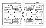
上述した実施形態では、各チップがリクエスターとして機能するチップリンクかレスポンダーとして機能するチップリンクかのいずれかを備えるものとしたが、これに限られず、各チップがリクエスターとして機能するチップリンクとレスポンダーとして機能するチップリンクとのいずれも備えるものとしてもよい。図5は、変形例のチップリンク接続の一例を示す説明図である。図示するように、チップ110とチップ120とがチップリンク接続されている。チップ110は、マスターとしてのプロセッサー112と、スレーブとしてのメモリー(コントローラーを含む、以下同じ)116と、ルーター117と、リクエスターとして機能するチップリンク118と、レスポンダーとして機能するチップリンク119とを備える。また、チップ120は、チップ110と同一の構成を備えているため、各構成要素はチップ110の各構成要素の符号に値10を加えた符号を付して、その説明を省略する。この例では、リクエスターとして機能するチップリンク118とレスポンダーとして機能するチップリンク129とがチップリンク接続されると共にリクエスターとして機能するチップリンク128とレスポンダーとして機能するチップリンク119とがチップリンク接続されている。また、プロセッサー112,122には、リクエストの送信先として、それぞれメモリー116(識別情報S11)やメモリー126(識別情報S12)が登録されている。そして、ルーター117,118の各ポート(図示省略)には、上述した実施形態と同様に、各ポートと接続先の識別情報とを対応付けて登録している。特に、チップ間の通信を行なうために、ルーター117のチップリンク118が接続されるポートにチップ120のメモリー126の識別情報S12を対応付け、チップリンク119が接続されるポートにチップ120のプロセッサー122の識別情報M12を対応付けて登録している。また、ルーター127のチップリンク128が接続されるポートにチップ110のメモリー116の識別情報S11を対応付け、チップリンク129が接続されるポートにチップ110のプロセッサー112の識別情報M11を対応付けて登録している。これにより、チップ110のプロセッサー112からチップ120のメモリー126へのリクエストが出力されると、ルーター117,チップリンク118,チップリンク129,ルーター127を順に介してメモリー126に到達し、メモリー126からレスポンスが出力されると、ルーター127,チップリンク129,チップリンク118,ルーター117を順に介してプロセッサー112に到達する。同様に、チップ120のプロセッサー122からチップ110のメモリー116へのリクエストが送信されると、ルーター127,チップリンク128,チップリンク119,ルーター117を順に介してメモリー116に到達する。また、メモリー116からレスポンスが送信されると、ルーター117,チップリンク119,チップリンク128,ルーター127を順に介してプロセッサー122に到達する。このように、リクエスターとして機能するチップリンクとレスポンダーとして機能するチップリンクとを各チップにそれぞれ設けて接続することで、各チップのマスターから接続先のチップのスレーブに相互にアクセスすることができる。
In the embodiment described above, each chip is provided with either a chip link that functions as a requester or a chip link that functions as a responder. However, the present invention is not limited to this, and a chip link in which each chip functions as a requester Any one of the chip links functioning as a responder may be provided. FIG. 5 is an explanatory diagram illustrating an example of a chip link connection according to a modification. As shown in the figure, the
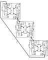
上述した実施形態では、印刷ヘッドコントローラー47とメインチップ31との2つのチップをチップリンク接続するものとしたが、これに限られず、3つ以上のチップをチップリンク接続するものとしてもよい。図6,7は、変形例のチップリンク接続の一例を示す説明図であり、チップ110,120,130の3つのチップがチップリンク接続される様子を示す。ここで、詳細な説明は省略するが、3つ以上の複数のチップをチップリンク接続した場合であっても、チップ内のマスターやスレーブ,ルーターはチップ内の通信と同様にチップ間の通信を行なうことができる。例えば、図6のチップ110のプロセッサー112(識別情報M11)からチップ130のメモリー136(識別情報S13)へのリクエストが送信されると、ルーター117,チップリンク118,チップリンク129,ルーター127,チップリンク128,チップリンク139,ルーター137を順に介してメモリー136に到達する。また、メモリー136からレスポンスが送信されると、ルーター137,チップリンク139,チップリンク128,ルーター127,チップリンク129,チップリンク118,ルーター117を順に介してプロセッサー112に到達する。なお、図6に示すように、チップ110(130)は他のチップに未接続のチップリンク118,119(138,139)を備えているから、それらのチップリンク118,119(138,139)に新たなチップを接続することで、システムを容易に拡張することができる。また、図7では、3つのチップ110,120,130をループ状にチップリンク接続することにより、少ないチップリンク数で図6と同様なチップ間の通信を実現している。なお、図7においても、いずれかのチップに未接続のチップリンクを設けておけば、システムを容易に拡張することができる。
In the embodiment described above, the two chips of the
上述した実施形態では、印刷ヘッドコントローラー47のプロセッサー52a〜52dが各ノズル列25毎にノズル24の制御を行なうものとしたが、これに限られず、ノズル24をいくつかのグループに分けてグループ毎に制御を行なうものとしてもよいし、各ノズル24をそれぞれ個別に制御するものとしてもよい。図8は、変形例の印刷ヘッドコントローラー150の構成を示す構成図である。変形例の印刷ヘッドコントローラー150は、図示するように、4つのノズル列25に対応する4つのサブチップ150a,150b,150c,150dを備え、これらがメインチップ31に対して直列的にチップリンク接続されている。このうちサブチップ150aは、ノズル列25Cの各ノズル24Cをそれぞれ個別に制御する複数のプロセッサー152aと、ルーター157aと、リクエスターとして機能するチップリンク158aと、レスポンダーとして機能するチップリンク158bとを備える。他のサブチップ150b,150c,150dも同様に構成されている。また、図示は省略するが、直列的に接続される各サブチップ150a,150b,150c,150dにおいて、前段側(メインチップ31側)のサブチップのレスポンダーとしてのチップリンクと、後段側のサブチップのリクエスターとしてのチップリンクとがそれぞれ順に接続されるものとした。また、サブチップ150aのリクエスターとしてのチップリンク158aは、メインチップ31(チップリンク39)に接続されている。これにより、各サブチップ150a〜dの各プロセッサーからメインチップ31内のメモリー(SDRAM35など)にアクセスすることができる。また、サブチップ150dのレスポンダーとしてのチップリンクは未接続となるから、新たなチップを接続することによりシステムを容易に拡張することができる。
In the above-described embodiment, the
上述した実施形態では、パラレル−シリアル変換を行なってパラレルデータをシリアルデータに変換してから接続先のチップに送信するものとしたが、これに限られず、パラレル−シリアル変換を行なわずにパラレルデータのままで送信するものとしてもよい。また、リクエストやレスポンスをパラレルデータとしたが、これに限られず、シリアルデータとしてもよい。 In the above-described embodiment, parallel-serial conversion is performed to convert parallel data into serial data, and then transmitted to the connection destination chip. However, the present invention is not limited to this, and parallel data without performing parallel-serial conversion. It may be transmitted as it is. Although the request and response are parallel data, the present invention is not limited to this, and serial data may be used.
上述した実施形態では、メインチップ31のバスクロックと印刷ヘッドコントローラー47のバスクロックとが異なるものとしたが、これに限られず、同じバスクロックとしてもよい。また、チップリンク58によりバスクロックを所定数倍の周波数としたクロック信号に基づいてリクエストにパラレル−シリアル変換を行なってチップリンク39に送信したりチップリンク39によりバスクロックを所定数倍の周波数としたクロック信号に基づいてレスポンスにパラレル−シリアル変換を行なってチップリンク58に送信したりするものとしたが、これに限られず、バスクロックよりも高い周波数に基づいてパラレル−シリアル変換を行なうものなどとしてもよい。
In the embodiment described above, the bus clock of the
上述した実施形態では、本発明のデバイスシステムとしての処理制御部30がプリンター20に搭載されるものとして説明したが、これに限られず、如何なる機器に搭載されるものとしてもよく、例えば、パーソナルコンピューターやゲーム機器などに搭載されるものなどとしてもよい。また、マスターとしてメインチップ31内のメインプロセッサー32や印刷ヘッドコントローラー47(プロセッサー52a〜52d)などを例示したが、プロセッサーに限られず、登録された送信先に対するリクエストを送信可能なものであれば如何なるものとしてもよい。そして、スレーブとしてSDRAMコントローラー34やSRAMコントローラー56などを例示したが、メモリーコントローラーに限られず、マスターからのリクエストに対するレスポンスを送信するものであれば如何なるものとしてもよい。さらに、複数のチップから構成されるデバイスシステムの形態とするものに限られず、他のチップと接続される各チップ単体の形態とするものとしてもよい。
In the above-described embodiment, the
20 プリンター、22 プリンター機構、23 印刷ヘッド、24,24C,24M,24Y,24K ノズル、25,25C,25M,25Y,25K ノズル列、26 各モーター、28 LCD、30 処理制御部、31 メインチップ、32 メインプロセッサー、33 DMAコントローラー、34 SDRAMコントローラー、35 SDRAM、36 SRAMコントローラー、36a SRAM、37 ルーター、39 チップリンク(Responder)、39a トランスミッター(Tx)、39b レシーバー(Rx)、41 カードコントローラー、43 I/Fコントローラー、45 LCDコントローラー、47 印刷ヘッドコントローラー、49 モーターコントローラー、52a,52b,52c,52d プロセッサー、56 SRAMコントローラー、56a SRAM、57 ルーター、58 チップリンク(Requester)、58a トランスミッター(Tx)、58b レシーバー(Rx)、110,120,130 チップ、112,122,132 プロセッサー、116,126,136 メモリー、117,127,137 ルーター、118,128,138 チップリンク(Requester)、119,129,139 チップリンク(Responder)、150 印刷ヘッドコントローラー、150a,150b,150c,150d サブチップ、152a プロセッサー、157a ルーター、158a チップリンク(Requester)、158b チップリンク(Responder)、CL チップリンク接続、MC メモリーカード、P31〜P35,P51〜P56 ポート、S 用紙。 20 printer, 22 printer mechanism, 23 print head, 24, 24C, 24M, 24Y, 24K nozzle, 25, 25C, 25M, 25Y, 25K nozzle row, 26 motors, 28 LCD, 30 processing control unit, 31 main chip, 32 main processor, 33 DMA controller, 34 SDRAM controller, 35 SDRAM, 36 SRAM controller, 36a SRAM, 37 router, 39 chip link (Responder), 39a transmitter (Tx), 39b receiver (Rx), 41 card controller, 43 I / F controller, 45 LCD controller, 47 print head controller, 49 motor controller, 52a, 52b, 52c, 52d processor, 56 SRAM Controller, 56a SRAM, 57 router, 58 chip link (Requester), 58a transmitter (Tx), 58b receiver (Rx), 110, 120, 130 chip, 112, 122, 132 processor, 116, 126, 136 memory, 117 , 127, 137 Router, 118, 128, 138 Chip Link (Requester), 119, 129, 139 Chip Link (Responder), 150 Print Head Controller, 150a, 150b, 150c, 150d Subchip, 152a Processor, 157a Router, 158a Chip Link (Requester), 158b Chip link (Responder), CL chip link connection, MC memory card, P31-P35, P51-P56 port, S paper.
Claims (8)
前記内部中継器に前記ポートを介して接続される第1の外部中継器と第2の外部中継器とを一組として、少なくとも該一組の外部中継器同士の接続により前記各チップが接続され、
前記マスターは、前記送信先として、自身が搭載されるチップ内のスレーブと、自身が搭載されるチップ内の前記第1の外部中継器を介して接続される接続先のチップ内のスレーブとが登録され、前記送信先に選択したスレーブの識別情報と自身の識別情報であるマスターの識別情報とを格納して前記リクエストを生成して送信し、
前記スレーブは、前記リクエスト内の前記マスターの識別情報を格納して前記レスポンスを生成して送信し、
前記内部中継器は、前記ポートに接続される接続先の識別情報と該ポートとの対応関係として、前記マスターの識別情報と該マスターに接続されるポートとの対応と、前記スレーブの識別情報と該スレーブに接続されるポートとの対応と、前記第1の外部中継器を介して接続される接続先のチップ内のスレーブの識別情報と該第1の外部中継器に接続されるポートとの対応と、前記第2の外部中継器を介して接続される接続先のチップ内のマスターの識別情報と該第2の外部中継器に接続されるポートとの対応とをそれぞれ記憶し、前記リクエストを受信すると該リクエスト内の前記スレーブの識別情報と前記対応関係とに基づいて選択したポートから該リクエストを送信し、前記レスポンスを受信すると該レスポンス内の前記マスターの識別情報と前記対応関係とに基づいて選択したポートから該レスポンスを送信し、
前記第1の外部中継器は、前記内部中継器から前記リクエストを受信すると接続先の前記第2の外部中継器に該リクエストを送信し、接続先の前記第2の外部中継器から前記レスポンスを受信すると前記内部中継器に該レスポンスを送信し、
前記第2の外部中継器は、接続先の前記第1の外部中継器から前記リクエストを受信すると該リクエストを前記内部中継器に送信し、前記内部中継器から前記レスポンスを受信すると該レスポンスを接続先の前記第1の外部中継器に送信する
デバイスシステム。 Connects a plurality of chips mounted with a master that transmits a request to a registered transmission destination, a slave that transmits a response to the request, and an internal repeater that is connected to the master and the slave via a port A device system comprising:
The first external repeater and the second external repeater connected to the internal repeater via the port as a set, and each chip is connected by connecting at least the set of external repeaters. ,
The master includes, as the transmission destination, a slave in a chip on which the master is mounted and a slave in a connection destination chip connected via the first external repeater in the chip on which the master is mounted. Registered and stored the identification information of the slave selected as the transmission destination and the identification information of the master that is the identification information of itself to generate and transmit the request,
The slave stores the identification information of the master in the request and generates and transmits the response,
The internal repeater has a correspondence relationship between identification information of a connection destination connected to the port and the port, correspondence between the identification information of the master and a port connected to the master, identification information of the slave, Correspondence between a port connected to the slave, identification information of a slave in a connection destination chip connected via the first external repeater, and a port connected to the first external repeater Storing the correspondence and the correspondence between the identification information of the master in the connection destination chip connected via the second external repeater and the port connected to the second external repeater; Is received from the port selected based on the identification information of the slave in the request and the corresponding relationship, and when the response is received, the identification of the master in the response is received. Transmitted the response from the port selected on the basis of the information and the correspondence relation,
When the first external repeater receives the request from the internal repeater, the first external repeater transmits the request to the second external repeater to be connected, and receives the response from the second external repeater to be connected. When receiving, send the response to the internal repeater,
The second external repeater transmits the request to the internal repeater when receiving the request from the first external repeater to which it is connected, and connects the response when receiving the response from the internal repeater A device system for transmitting to the first external repeater.
前記第1の外部中継器は、接続先の前記第2の外部中継器から前記レスポンスを受信すると自身が搭載されるチップのバスクロックの周波数に合わせて前記内部中継器に該レスポンスを送信し、
前記第2の外部中継器は、接続先の前記第1の外部中継器から前記リクエストを受信すると自身が搭載されるチップのバスクロックの周波数に合わせて前記内部中継器に該リクエストを送信する
デバイスシステム。 The device system according to claim 1, wherein the chips having different bus clock frequencies are connected.
The first external repeater transmits the response to the internal repeater according to the frequency of the bus clock of the chip on which the first external repeater receives the response from the second external repeater connected to the first repeater,
When the second external repeater receives the request from the first external repeater connected to the second external repeater, the second external repeater transmits the request to the internal repeater according to the bus clock frequency of the chip on which the second external repeater is mounted. system.
前記第1の外部中継器は、前記内部中継器から前記リクエストを受信すると自身が搭載されるチップのバスクロックの周波数よりも高い周波数に基づいてパラレル形式からシリアル形式に変換するパラレルシリアル変換を施して接続先の前記第2の外部中継器に該リクエストを送信し、接続先の前記第2の外部中継器から前記レスポンスを受信すると自身が搭載されるチップのバスクロックの周波数に基づいてシリアル形式からパラレル形式に変換するシリアルパラレル変換を施して前記内部中継器に該レスポンスを送信し、
前記第2の外部中継器は、接続先の前記第1の外部中継器から前記リクエストを受信すると自身が搭載されるチップのバスクロックの周波数に基づいてシリアル形式からパラレル形式に変換するシリアルパラレル変換を施して該リクエストを前記内部中継器に送信し、前記内部中継器から前記レスポンスを受信すると自身が搭載されるチップのバスクロックの周波数よりも高い周波数に基づいてパラレル形式からシリアル形式に変換するパラレルシリアル変換を施して該レスポンスを接続先の前記第1の外部中継器に送信する
デバイスシステム。 The device system according to claim 1, wherein communication within the chip is performed in parallel format data.
When the first external repeater receives the request from the internal repeater, the first external repeater performs parallel-serial conversion for converting from a parallel format to a serial format based on a frequency higher than the bus clock frequency of the chip on which the request is received. When the request is transmitted to the second external repeater at the connection destination and the response is received from the second external repeater at the connection destination, the serial format is determined based on the frequency of the bus clock of the chip on which the request is mounted. Send the response to the internal repeater with serial to parallel conversion to convert from parallel to
When the second external repeater receives the request from the first external repeater connected to the second external repeater, the second external repeater converts the serial format to the parallel format based on the bus clock frequency of the chip on which the second external repeater is mounted. The request is transmitted to the internal repeater, and when the response is received from the internal repeater, the parallel format is converted to the serial format based on a frequency higher than the bus clock frequency of the chip on which the request is mounted. A device system that performs parallel-serial conversion and transmits the response to the first external repeater that is a connection destination.
前記マスターとして前記複数のノズルからの液滴の吐出を制御するプロセッサーを備えると共に前記スレーブとして前記液滴の吐出に関するデータを記憶するメモリーへの該データの読み書きを制御するメモリーコントローラーを備える
デバイスシステム。 5. The device system according to claim 4, further comprising an ejection head having a plurality of nozzles for ejecting liquid droplets, and mounted on an image forming apparatus that forms an image on the medium by ejecting liquid droplets from the nozzles. And
A device system comprising: a processor that controls ejection of droplets from the plurality of nozzles as the master; and a memory controller that controls reading and writing of the data to a memory that stores data relating to ejection of the droplets as the slave.
前記内部中継器に前記ポートを介して接続される第1の外部中継器と第2の外部中継器とを一組として、少なくとも該一組の外部中継器同士の接続により他のチップと接続され、
前記マスターは、前記送信先として、前記チップ内のスレーブと、前記第1の外部中継器を介して接続される接続先のチップ内のスレーブとが登録され、前記送信先に選択したスレーブの識別情報と自身の識別情報であるマスターの識別情報とを格納して前記リクエストを生成して送信し、
前記スレーブは、前記リクエスト内の前記マスターの識別情報を格納して前記レスポンスを生成して送信し、
前記内部中継器は、前記ポートに接続される接続先の識別情報と該ポートとの対応関係として、前記マスターの識別情報と該マスターに接続されるポートとの対応と、前記スレーブの識別情報と該スレーブに接続されるポートとの対応と、前記第1の外部中継器を介して接続される接続先のチップ内のスレーブの識別情報と該第1の外部中継器に接続されるポートとの対応と、前記第2の外部中継器を介して接続される接続先のチップ内のマスターの識別情報と該第2の外部中継器に接続されるポートとの対応とをそれぞれ記憶し、前記リクエストを受信すると該リクエスト内の前記スレーブの識別情報と前記対応関係とに基づいて選択したポートから該リクエストを送信し、前記レスポンスを受信すると該レスポンス内の前記マスターの識別情報と前記対応関係とに基づいて選択したポートから該レスポンスを送信し、
前記第1の外部中継器は、前記内部中継器から前記リクエストを受信すると接続先のチップ内の前記第2の外部中継器に該リクエストを送信し、接続先のチップ内の前記第2の外部中継器から前記レスポンスを受信すると前記内部中継器に該レスポンスを送信し、
前記第2の外部中継器は、接続先のチップ内の前記第1の外部中継器から前記リクエストを受信すると該リクエストを前記内部中継器に送信し、前記内部中継器から前記レスポンスを受信すると該レスポンスを接続先のチップ内の前記第1の外部中継器に送信する
チップ。 A chip on which a master that transmits a request for a registered transmission destination, a slave that transmits a response to the request, and an internal repeater connected to the master and the slave via a port,
A set of the first external repeater and the second external repeater connected to the internal repeater via the port is connected to another chip by connecting at least the set of external repeaters. ,
The master registers the slave in the chip and the slave in the connection destination chip connected via the first external repeater as the transmission destination, and identifies the slave selected as the transmission destination. Storing the information and the identification information of the master that is its own identification information, generating and sending the request,
The slave stores the identification information of the master in the request and generates and transmits the response,
The internal repeater has a correspondence relationship between identification information of a connection destination connected to the port and the port, correspondence between the identification information of the master and a port connected to the master, identification information of the slave, Correspondence between a port connected to the slave, identification information of a slave in a connection destination chip connected via the first external repeater, and a port connected to the first external repeater Storing the correspondence and the correspondence between the identification information of the master in the connection destination chip connected via the second external repeater and the port connected to the second external repeater; Is received from the port selected based on the identification information of the slave in the request and the corresponding relationship, and when the response is received, the identification of the master in the response is received. Transmitted the response from the port selected on the basis of the information and the correspondence relation,
When the first external repeater receives the request from the internal repeater, the first external repeater transmits the request to the second external repeater in the connection destination chip, and the second external repeater in the connection destination chip. When the response is received from the repeater, the response is transmitted to the internal repeater,
The second external repeater transmits the request to the internal repeater when receiving the request from the first external repeater in the connected chip, and receives the response from the internal repeater when the request is received. A chip that transmits a response to the first external repeater in the chip to be connected.
Priority Applications (1)
| Application Number | Priority Date | Filing Date | Title |
|---|---|---|---|
| JP2011042446A JP2012181585A (en) | 2011-02-28 | 2011-02-28 | Device system and chip |
Applications Claiming Priority (1)
| Application Number | Priority Date | Filing Date | Title |
|---|---|---|---|
| JP2011042446A JP2012181585A (en) | 2011-02-28 | 2011-02-28 | Device system and chip |
Publications (1)
| Publication Number | Publication Date |
|---|---|
| JP2012181585A true JP2012181585A (en) | 2012-09-20 |
Family
ID=47012751
Family Applications (1)
| Application Number | Title | Priority Date | Filing Date |
|---|---|---|---|
| JP2011042446A Pending JP2012181585A (en) | 2011-02-28 | 2011-02-28 | Device system and chip |
Country Status (1)
| Country | Link |
|---|---|
| JP (1) | JP2012181585A (en) |
Cited By (1)
| Publication number | Priority date | Publication date | Assignee | Title |
|---|---|---|---|---|
| JP2021026767A (en) * | 2019-07-31 | 2021-02-22 | ベイジン バイドゥ ネットコム サイエンス アンド テクノロジー カンパニー リミテッド | Data memory access method, apparatus, electronic device and computer-readable storage medium |
Citations (13)
| Publication number | Priority date | Publication date | Assignee | Title |
|---|---|---|---|---|
| JPS6344267A (en) * | 1986-08-12 | 1988-02-25 | Nec Corp | Intermodule bus system |
| JPH0381862A (en) * | 1989-08-24 | 1991-04-08 | Fuji Heavy Ind Ltd | Equipment and method for communication of vehicle-mounted network |
| JPH1115804A (en) * | 1997-04-30 | 1999-01-22 | Nec Corp | Topology information exchanging device and machine-readable recording medium for recording program |
| JP2000071434A (en) * | 1998-08-27 | 2000-03-07 | Seiko Epson Corp | Printing device and printing method |
| JP2003114879A (en) * | 2001-06-28 | 2003-04-18 | Fujitsu Ltd | How to balance message traffic with multi-chassis computer systems |
| JP2003198356A (en) * | 2001-12-25 | 2003-07-11 | Hitachi Ltd | Semiconductor chip and integrated circuit |
| US20030225938A1 (en) * | 2002-05-28 | 2003-12-04 | Newisys, Inc., A Delaware Corporation | Routing mechanisms in systems having multiple multi-processor clusters |
| US20030225909A1 (en) * | 2002-05-28 | 2003-12-04 | Newisys, Inc. | Address space management in systems having multiple multi-processor clusters |
| JP2006146391A (en) * | 2004-11-17 | 2006-06-08 | Hitachi Ltd | Multiprocessor system |
| JP2006518885A (en) * | 2002-11-05 | 2006-08-17 | ニューイシス・インコーポレーテッド | Transaction processing performed using multiple protocol engines in a system with multiple multiprocessor clusters |
| JP2009032857A (en) * | 2007-07-26 | 2009-02-12 | Hitachi Ltd | Semiconductor integrated circuit and semiconductor device |
| JP2009251652A (en) * | 2008-04-01 | 2009-10-29 | Mitsubishi Electric Corp | Multi-core system |
| JP2010052200A (en) * | 2008-08-27 | 2010-03-11 | Seiko Epson Corp | Ejection amount counting device and fluid ejection device |
-
2011
- 2011-02-28 JP JP2011042446A patent/JP2012181585A/en active Pending
Patent Citations (13)
| Publication number | Priority date | Publication date | Assignee | Title |
|---|---|---|---|---|
| JPS6344267A (en) * | 1986-08-12 | 1988-02-25 | Nec Corp | Intermodule bus system |
| JPH0381862A (en) * | 1989-08-24 | 1991-04-08 | Fuji Heavy Ind Ltd | Equipment and method for communication of vehicle-mounted network |
| JPH1115804A (en) * | 1997-04-30 | 1999-01-22 | Nec Corp | Topology information exchanging device and machine-readable recording medium for recording program |
| JP2000071434A (en) * | 1998-08-27 | 2000-03-07 | Seiko Epson Corp | Printing device and printing method |
| JP2003114879A (en) * | 2001-06-28 | 2003-04-18 | Fujitsu Ltd | How to balance message traffic with multi-chassis computer systems |
| JP2003198356A (en) * | 2001-12-25 | 2003-07-11 | Hitachi Ltd | Semiconductor chip and integrated circuit |
| US20030225938A1 (en) * | 2002-05-28 | 2003-12-04 | Newisys, Inc., A Delaware Corporation | Routing mechanisms in systems having multiple multi-processor clusters |
| US20030225909A1 (en) * | 2002-05-28 | 2003-12-04 | Newisys, Inc. | Address space management in systems having multiple multi-processor clusters |
| JP2006518885A (en) * | 2002-11-05 | 2006-08-17 | ニューイシス・インコーポレーテッド | Transaction processing performed using multiple protocol engines in a system with multiple multiprocessor clusters |
| JP2006146391A (en) * | 2004-11-17 | 2006-06-08 | Hitachi Ltd | Multiprocessor system |
| JP2009032857A (en) * | 2007-07-26 | 2009-02-12 | Hitachi Ltd | Semiconductor integrated circuit and semiconductor device |
| JP2009251652A (en) * | 2008-04-01 | 2009-10-29 | Mitsubishi Electric Corp | Multi-core system |
| JP2010052200A (en) * | 2008-08-27 | 2010-03-11 | Seiko Epson Corp | Ejection amount counting device and fluid ejection device |
Cited By (2)
| Publication number | Priority date | Publication date | Assignee | Title |
|---|---|---|---|---|
| JP2021026767A (en) * | 2019-07-31 | 2021-02-22 | ベイジン バイドゥ ネットコム サイエンス アンド テクノロジー カンパニー リミテッド | Data memory access method, apparatus, electronic device and computer-readable storage medium |
| US11169718B2 (en) | 2019-07-31 | 2021-11-09 | Beijing Baidu Netcom Science And Technology Co., Ltd. | Data access method and apparatus |
Similar Documents
| Publication | Publication Date | Title |
|---|---|---|
| EP2072260B1 (en) | Head element substrate, recording head, and recording apparatus | |
| JP5842408B2 (en) | Image forming apparatus, image forming apparatus control method, image processing apparatus, and image processing apparatus control method | |
| US20120069398A1 (en) | Printing system and printing device | |
| WO2000058102A1 (en) | Printer | |
| JP6606389B2 (en) | Recording control apparatus, recording apparatus, and data processing method | |
| JP2012181585A (en) | Device system and chip | |
| EP1217576B1 (en) | Method and apparatus for formatting and serving inkjet image data | |
| JP5446248B2 (en) | Image forming apparatus, image forming system, and head device | |
| JP5799660B2 (en) | Printing apparatus and printing apparatus control method | |
| JP5470834B2 (en) | Image forming apparatus | |
| US20050225589A1 (en) | Printing device, printing method, and program product therefor | |
| US8917421B2 (en) | Printing apparatus and method of controlling printing apparatus | |
| CN101306606A (en) | Data transmission device, its control method, and data processing method | |
| US9953251B2 (en) | Image processing apparatus and image processing method for executing image processing using multiple serial image processing units to process different colors | |
| JP2012178122A (en) | Device system and repeater | |
| JP5078540B2 (en) | Recording apparatus and data transfer method | |
| JP2008100483A (en) | Head substrate, recording head, and recording apparatus | |
| US8491077B2 (en) | Printing device and printing method | |
| JP3871177B2 (en) | Data communication apparatus and data communication method | |
| JP6559033B2 (en) | Recording control apparatus, recording apparatus, and data processing method | |
| JP5082686B2 (en) | Print head control device | |
| JP2010240937A (en) | Image forming apparatus, image forming system, and image forming method | |
| JP5233649B2 (en) | Image forming apparatus | |
| JP2022141103A (en) | recording device | |
| US6509978B1 (en) | Method and apparatus for formatting bitmapped image data |
Legal Events
| Date | Code | Title | Description |
|---|---|---|---|
| A621 | Written request for application examination |
Free format text: JAPANESE INTERMEDIATE CODE: A621 Effective date: 20140129 |
|
| A977 | Report on retrieval |
Free format text: JAPANESE INTERMEDIATE CODE: A971007 Effective date: 20141028 |
|
| A131 | Notification of reasons for refusal |
Free format text: JAPANESE INTERMEDIATE CODE: A131 Effective date: 20141111 |
|
| A521 | Written amendment |
Free format text: JAPANESE INTERMEDIATE CODE: A523 Effective date: 20141225 |
|
| A02 | Decision of refusal |
Free format text: JAPANESE INTERMEDIATE CODE: A02 Effective date: 20150120 |