JP2012189708A - Imaging device - Google Patents
Imaging device Download PDFInfo
- Publication number
- JP2012189708A JP2012189708A JP2011052002A JP2011052002A JP2012189708A JP 2012189708 A JP2012189708 A JP 2012189708A JP 2011052002 A JP2011052002 A JP 2011052002A JP 2011052002 A JP2011052002 A JP 2011052002A JP 2012189708 A JP2012189708 A JP 2012189708A
- Authority
- JP
- Japan
- Prior art keywords
- lens
- imaging
- image sensor
- image
- unit
- Prior art date
- Legal status (The legal status is an assumption and is not a legal conclusion. Google has not performed a legal analysis and makes no representation as to the accuracy of the status listed.)
- Granted
Links
Images








Classifications
-
- G—PHYSICS
- G02—OPTICS
- G02B—OPTICAL ELEMENTS, SYSTEMS OR APPARATUS
- G02B3/00—Simple or compound lenses
- G02B3/0006—Arrays
- G02B3/0037—Arrays characterized by the distribution or form of lenses
- G02B3/0056—Arrays characterized by the distribution or form of lenses arranged along two different directions in a plane, e.g. honeycomb arrangement of lenses
-
- G—PHYSICS
- G02—OPTICS
- G02B—OPTICAL ELEMENTS, SYSTEMS OR APPARATUS
- G02B27/00—Optical systems or apparatus not provided for by any of the groups G02B1/00 - G02B26/00, G02B30/00
- G02B27/0075—Optical systems or apparatus not provided for by any of the groups G02B1/00 - G02B26/00, G02B30/00 with means for altering, e.g. increasing, the depth of field or depth of focus
-
- G—PHYSICS
- G02—OPTICS
- G02B—OPTICAL ELEMENTS, SYSTEMS OR APPARATUS
- G02B3/00—Simple or compound lenses
- G02B3/0006—Arrays
- G02B3/0037—Arrays characterized by the distribution or form of lenses
- G02B3/0062—Stacked lens arrays, i.e. refractive surfaces arranged in at least two planes, without structurally separate optical elements in-between
- G02B3/0068—Stacked lens arrays, i.e. refractive surfaces arranged in at least two planes, without structurally separate optical elements in-between arranged in a single integral body or plate, e.g. laminates or hybrid structures with other optical elements
-
- G—PHYSICS
- G03—PHOTOGRAPHY; CINEMATOGRAPHY; ANALOGOUS TECHNIQUES USING WAVES OTHER THAN OPTICAL WAVES; ELECTROGRAPHY; HOLOGRAPHY
- G03B—APPARATUS OR ARRANGEMENTS FOR TAKING PHOTOGRAPHS OR FOR PROJECTING OR VIEWING THEM; APPARATUS OR ARRANGEMENTS EMPLOYING ANALOGOUS TECHNIQUES USING WAVES OTHER THAN OPTICAL WAVES; ACCESSORIES THEREFOR
- G03B35/00—Stereoscopic photography
- G03B35/08—Stereoscopic photography by simultaneous recording
Landscapes
- Physics & Mathematics (AREA)
- General Physics & Mathematics (AREA)
- Optics & Photonics (AREA)
- Studio Devices (AREA)
- Transforming Light Signals Into Electric Signals (AREA)
- Solid State Image Pick-Up Elements (AREA)
- Stereoscopic And Panoramic Photography (AREA)
Abstract
【課題】レンズアレイを含む光学系を利用して撮影した画像において、明るさのむらを軽減することが可能な撮像装置を提供する。
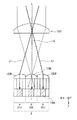
【解決手段】撮像レンズ、レンズアレイおよびイメージセンサ13を用いて、視点方向を分離しつつ画像取得を行う撮像装置において、レンズアレイとして、複数の第1レンズ部S1および第2レンズ部S2を有するものを用いる。撮像レンズおよび第1レンズ部S1を通過した主光線Lを、イメージセンサ13における各画素Pの受光面130bに略垂直に入射させることができる。イメージセンサ13において局所的な光損失が低減される。
【選択図】図13An image pickup apparatus capable of reducing uneven brightness in an image shot using an optical system including a lens array.
An imaging apparatus that acquires an image while separating viewpoint directions using an imaging lens, a lens array, and an image sensor 13 includes a plurality of first lens portions S1 and second lens portions S2 as lens arrays. Use things. The principal ray L that has passed through the imaging lens and the first lens unit S1 can be incident substantially perpendicularly on the light receiving surface 130b of each pixel P in the image sensor 13. Local light loss is reduced in the image sensor 13.
[Selection] Figure 13
Description
本発明は、レンズアレイを用いた撮像装置に関する。 The present invention relates to an imaging apparatus using a lens array.
従来、様々な撮像装置が提案され、開発されている(非特許文献1)。また、撮像データに対し、所定の画像処理を施して出力するようにした撮像装置も提案されている。例えば、特許文献1および非特許文献1には、「Light Field Photography」と呼ばれる手法を用いた撮像装置が提案されている。この撮像装置は、撮像レンズとイメージセンサとの間に(撮像レンズの焦点面に)、レンズアレイを配置したものである。これにより、レンズアレイ上に結像する被写体の映像を、イメージセンサにおいて、各視点方向の光線に分離しつつ受光し、同時刻に多視点の画像を取得することができる。
Conventionally, various imaging devices have been proposed and developed (Non-Patent Document 1). There has also been proposed an imaging apparatus that performs predetermined image processing on imaging data and outputs the processed data. For example,
上記のような撮像装置では、レンズアレイにおける1つのレンズに、イメージセンサ上の複数の画素が割り当てられており、そのレンズに割り当てられた画素数分の視点画像を取得可能である。例えば、1つのレンズが3×3の画素(9画素)に割り当てられている場合には、9視点分の画像を取得することができる。これらの視点画像は、例えば立体映像表示の際の左右の視点画像として利用可能である。 In the imaging apparatus as described above, a plurality of pixels on the image sensor are assigned to one lens in the lens array, and viewpoint images corresponding to the number of pixels assigned to the lens can be acquired. For example, when one lens is assigned to 3 × 3 pixels (9 pixels), images for nine viewpoints can be acquired. These viewpoint images can be used as, for example, left and right viewpoint images when displaying a stereoscopic video.
しかしながら、撮像レンズとイメージセンサとの間にレンズアレイを配設した場合、画素位置に応じて受光量が異なり、明るさにむらが生じるという問題がある。これらは撮影画像における画質劣化を招くため、改善が望まれる。 However, when a lens array is disposed between the imaging lens and the image sensor, there is a problem in that the amount of received light varies depending on the pixel position, resulting in uneven brightness. Since these cause deterioration of image quality in the photographed image, improvement is desired.
本発明はかかる問題点に鑑みてなされたもので、その目的は、レンズアレイを含む光学系を利用して撮影した画像において、明るさのむらを軽減することが可能な撮像装置を提供することにある。 The present invention has been made in view of such problems, and an object thereof is to provide an imaging apparatus capable of reducing uneven brightness in an image captured using an optical system including a lens array. is there.
本発明の撮像装置は、撮像レンズと、撮像レンズの結像面に設けられたレンズアレイを有する光学系と、撮像レンズおよび光学系の通過光線を受光して撮像データを取得する撮像素子とを備えたものである。光学系は、レンズアレイを構成する各レンズを通過する主光線を、各レンズの光軸に近づく方向に向けて屈折させるように構成されている。 An imaging apparatus according to the present invention includes an imaging lens, an optical system having a lens array provided on an imaging surface of the imaging lens, and an imaging element that receives imaging light and a passing ray of the optical system and acquires imaging data. It is provided. The optical system is configured to refract chief rays passing through each lens constituting the lens array in a direction approaching the optical axis of each lens.
本発明の撮像装置では、撮像レンズを通過した被写体からの光線は、レンズアレイによって視点方向毎に分離され、撮像素子において受光される(撮像データが得られる)。レンズアレイを含む光学系が、各レンズを通過する主光線を、各レンズの光軸に近づく方向に向けて屈折させることにより、撮像素子の受光面に略直交する方向に導くことができる。 In the imaging apparatus of the present invention, the light beam from the subject that has passed through the imaging lens is separated for each viewpoint direction by the lens array, and is received by the imaging device (imaging data is obtained). An optical system including a lens array can refract chief rays passing through each lens toward a direction approaching the optical axis of each lens, thereby guiding the principal ray in a direction substantially orthogonal to the light receiving surface of the image sensor.
本発明の撮像装置によれば、撮像レンズ、レンズアレイおよび撮像素子を備え、レンズアレイを含む光学系が、レンズアレイにおける各レンズを通過する主光線を、その光軸に近づく方向に向けて屈折させるように構成されている。光学系からの主光線を、撮像素子の受光面に対して略直交する方向に導くことができ、これにより、撮像素子では局所的な光損失を低減することができる。よって、レンズアレイを含む光学系を利用して撮影した画像において、明るさのむらを軽減することが可能となる。 According to the imaging apparatus of the present invention, the imaging system includes an imaging lens, a lens array, and an imaging device, and an optical system including the lens array refracts principal rays passing through each lens in the lens array toward a direction approaching the optical axis. It is configured to let you. The chief ray from the optical system can be guided in a direction substantially perpendicular to the light receiving surface of the image sensor, and thereby local light loss can be reduced in the image sensor. Therefore, uneven brightness can be reduced in an image captured using an optical system including a lens array.
以下、本発明の実施の形態について、図面を参照して詳細に説明する。尚、説明は以下の順序で行う。
1.第1の実施の形態(レンズアレイ自体に所定のレンズ面を設けた例)
2.変形例1(複数のレンズアレイで構成した例)
3.変形例2(レンズアレイとイメージセンサとを一体化した例)
4.第2の実施の形態(オンチップレンズを画素位置に応じて偏芯させた例)
5.変形例3(割り当て画素を増やした場合のオンチップレンズ偏芯の例)
6.変形例4(裏面照射型のイメージセンサの例)
Hereinafter, embodiments of the present invention will be described in detail with reference to the drawings. The description will be given in the following order.
1. First Embodiment (Example in which a predetermined lens surface is provided on the lens array itself)
2. Modification 1 (example configured with a plurality of lens arrays)
3. Modification 2 (example in which a lens array and an image sensor are integrated)
4). Second Embodiment (Example in which an on-chip lens is decentered according to a pixel position)
5. Modification 3 (Example of on-chip lens eccentricity when the number of assigned pixels is increased)
6). Modification 4 (Example of back-illuminated image sensor)
<第1の実施の形態>
[全体構成]
図1は、本発明の一実施の形態に係る撮像装置(撮像装置1)の全体構成を表すものである。撮像装置1は、いわゆる単眼方式のライトフィールドカメラであり、被写体2を撮像して所定の画像処理を施すことにより、視点画像としての画像データDoutを出力するものである。この撮像装置1は、撮像レンズ11と、レンズアレイ12Aと、イメージセンサ13と、画像処理部14と、イメージセンサ駆動部15と、制御部16とを備える。尚、以下では、光軸Z1に沿った方向をZとし、光軸Z1に直交する面内において、水平方向(横方向)をX、垂直方向(縦方向)をYとする。
<First Embodiment>
[overall structure]
FIG. 1 shows the overall configuration of an imaging apparatus (imaging apparatus 1) according to an embodiment of the present invention. The
撮像レンズ11は、被写体2を撮像するためのメインレンズであり、例えば、ビデオカメラやスチルカメラ等で使用される一般的な撮像レンズにより構成されている。この撮像レンズ11の光入射側(または光出射側)には、開口絞り10が配設されている。
The
レンズアレイ12Aは、撮像レンズ11の焦点面(結像面)に配置されることにより、入射光線の視点方向を分離するための光学系である。レンズアレイ12Aは、後述するマイクロレンズ12A1がX方向およびY方向に沿って複数個2次元配置されたものである。これら複数のマイクロレンズ12A1は、例えばフォトレジスト等の樹脂材料よりなり、ガラスやプラスチック等よりなる基板上に、例えばレジストリフロー法やナノインプリント法を用いて、形成されたものである。あるいは、ガラスなどの基板の主面にエッチング処理を施して形成されたものであってもよい。このレンズアレイ12Aの光出射側には、イメージセンサ13が配設されている。
The lens array 12 </ b> A is an optical system for separating the viewpoint direction of incident light by being disposed on the focal plane (imaging plane) of the
イメージセンサ13は、レンズアレイ12Aを通過した光線を受光して撮像データD0を取得するものである。このイメージセンサ13は、複数の画素がマトリクス状に(X方向およびY方向に沿って)配置したものであり、CCD(Charge Coupled Device:電荷結合素子)またはCMOS(Complementary Metal-Oxide Semiconductor)イメージセンサなどの固体撮像素子により構成されている。このイメージセンサ13の光入射側(レンズアレイ12の側)には、後述するカラーフィルタ層132およびオンチップレンズ133が設けられている。
The
画像処理部14は、イメージセンサ13において取得された撮像データD0に対して所定の画像処理を施し、例えば視点画像としての画像データDoutを出力するものである。図2に、画像処理部14の構成例について示す。画像処理部14は、例えば、視差画像生成部140と画像補正処理部142を有している。この画像処理部14の具体的な画像処理動作については後述する。
The
イメージセンサ駆動部15は、イメージセンサ13を駆動してその露光や読み出しの制御を行うものである。
The image
制御部16は、画像処理部14およびイメージセンサ駆動部15の動作を制御するものであり、例えばマイクロコンピュータなどにより構成されている。
The
(レンズアレイ12Aの詳細構成例)
図3(A)は、レンズアレイ12Aの斜視構成について、イメージセンサ13と共に示したものであり、図3(B)は、1つのマイクロレンズ12A1と、それに割り当てられる画素との対応関係を表したものである。レンズアレイ12Aは、光入射面(撮像レンズ11側の面)に、XY方向に2次元配置された複数の第1レンズ部S1を有しており、光出射面(イメージセンサ13側の面)には、それぞれが、各第1レンズ部S1と正対する(同軸上に設けられた)複数の第2レンズ部S2を有している。本実施の形態では、レンズアレイ12Aにおいて、互いに正対する第1レンズ部S1および第2レンズ部S2が、1つのマイクロレンズ12A1を構成している。尚、図3(A)では、簡便化のため、レンズアレイ12Aとして、XY方向に3×3の配列で設けられた計9つのマイクロレンズ12A1のみを示し、イメージセンサ13としては、そのようなレンズアレイ12Aに対応する9×9の画素Pからなる領域(9つのブロック領域U)についてのみ示している。
(Detailed configuration example of the
FIG. 3A shows the perspective configuration of the
第1レンズ部S1は、例えば撮像レンズ11の焦点面に配置され、撮像レンズ11から入射した光線を、複数の視点方向に分離しつつイメージセンサ13へ向かう方向に導くようになっている。第2レンズ部S2は、第1レンズ部S1を通過した主光線を各マイクロレンズ12A1(第1レンズ部S1)の光軸に近づく方向に向けて屈折させる機能を有する。
The first lens unit S1 is disposed, for example, on the focal plane of the
詳細には、マイクロレンズ12A1において、第1レンズ部S1の主面(主平面)に第2レンズ部S2の焦点面、第2レンズ部S2の主面に第1レンズ部S1の焦点面がそれぞれ配されるように、第1レンズ部S1および第2レンズ部S2が設けられている。正対する第1レンズ部S1および第2レンズ部S2において、それぞれの主面と焦点面とがこのような関係で配置されていれば、レンズ形状(物体側,像側の各面の凹凸およびその曲率)やレンズ材料は特に限定されない。但し、ここでは、第1レンズ部S1が、撮像レンズ11側に凸面を向けたレンズ形状、第2レンズ部S2が、イメージセンサ13側に凸面を向けたレンズ形状を有している場合について説明する。
Specifically, in the microlens 12A1, the focal plane of the second lens unit S2 is formed on the main surface (main plane) of the first lens unit S1, and the focal plane of the first lens unit S1 is formed on the main surface of the second lens unit S2. A first lens unit S1 and a second lens unit S2 are provided so as to be arranged. In the first lens portion S1 and the second lens portion S2 that face each other, if the respective principal surfaces and focal planes are arranged in such a relationship, the lens shape (the unevenness of each surface on the object side and the image side, and its The curvature and the lens material are not particularly limited. However, here, the case where the first lens portion S1 has a lens shape with a convex surface facing the
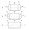
本実施の形態では、このような第1レンズ部S1および第2レンズ部S2が一体的に設けられている(一体化構造を有している)。図4(A)〜(C)に、第1レンズ部S1および第2レンズ部S2の一体化構造の一例を示す。図4(A),(B)に示したように、第1レンズ部S1および第2レンズ部S2は、例えばガラスやプラスチックなどの基板120の両面に、例えばフォトレジストなどの樹脂材料からなるレンズ層121が設けられた構造とすることができる。この場合、第1レンズ部S1および第2レンズ部S2はそれぞれ、図4(A)のように平凸形状であってもよいし、図4(B)のように凹凸形状であってもよい。あるいは図示はしないが、両凸形状、両凹形状などの形状としてもよい。第1レンズ部S1および第2レンズ部S2の各レンズ形状は、使用される樹脂材料の屈折率等を考慮して適切に設定されればよい。また、第1レンズ部S1および第2レンズ部S2は、単層構造であってもよいし、異なる材料が積層された多層構造となっていてもよい。また、上記のような配置関係(互いの主面と焦点面とが一致する位置関係)を有してさえいれば、第1レンズ部S1および第2レンズ部S2間において、レンズ形状やレンズ材料が互いに同一である必要はなく、互いに異なっていてもよい。
In the present embodiment, the first lens unit S1 and the second lens unit S2 are integrally provided (having an integrated structure). 4A to 4C show an example of an integrated structure of the first lens unit S1 and the second lens unit S2. As shown in FIGS. 4A and 4B, the first lens portion S1 and the second lens portion S2 are lenses made of a resin material such as a photoresist on both surfaces of a
あるいは、図4(C)に示したように、基板120(レンズ基材)の両面をエッチングによって直にパターニングすることにより、レンズ形状を作り込んだものであってもよい。 Alternatively, as shown in FIG. 4C, the lens shape may be formed by directly patterning both surfaces of the substrate 120 (lens base material) by etching.
上記のような第1レンズ部S1および第2レンズ部S2を有するレンズアレイ12Aの光出射側には、所定の空隙を介してイメージセンサ13が配置されている(イメージセンサ13が、レンズアレイ12Aの通過光線を受光可能な位置に配置されている)。レンズアレイ12Aを構成する1つのマイクロレンズ12A1には、イメージセンサ13におけるm×nの画素P(ブロック領域U)が割り当てられて配置されている。マイクロレンズ12A1のXY平面形状は、ブロック領域Uに等しい方形状となっている。m,nは1以上の整数であり(但し、m=n=1の場合は除く)、例えばm=nとなる正方形のブロック領域Uに、XY平面形状が正方形となるマイクロレンズ12A1が対向配置されている。m×nの値が大きくなるに従って、即ち1つのマイクロレンズに割り当てられる画素Pの数が多くなるに従って、得られる視点画像数が多くなる(分離可能な視点数が増える)。一方、レンズへの割り当て画素Pの数が少なくなる(m×nの値が小さくなる)に従って、各視点画像における画素数(解像度)が高くなる。ここでは、一例として、1つのマイクロレンズ12A1に3×3(m=n=3)の画素Pよりなるブロック領域Uが割り当てられた場合を例に挙げて説明する。
The
(イメージセンサ13およびオンチップレンズの構成例)
図5は、イメージセンサ13およびオンチップレンズ133の断面構成を表したものである。イメージセンサ13は、例えばPINフォトダイオードなどの光電変換素子を含むセンサ部130上に、配線層131とカラーフィルタ層132がこの順に積層されたものである。イメージセンサ13のカラーフィルタ層132の側には、集光用レンズとしてのオンチップレンズ133が画素P毎に設けられている。このイメージセンサ13は、センサ部130の受光面上に配線層131を有する、いわゆる表面照射型のCMOSイメージセンサである。
(Configuration example of
FIG. 5 illustrates a cross-sectional configuration of the
カラーフィルタ層132としては、例えば、赤(R:Red)、緑(G:Green)および青(B:Blue)の各色のフィルタが例えば1:2:1の比率で配列(ベイヤー配列)してなるものが用いられる。
As the
図6は、マイクロレンズ12A1、オンチップレンズ133およびイメージセンサ13のXZ断面構成を表したものである。詳細には、マイクロレンズ12A1の光軸Z2を通るXZ断面(ブロック領域Uの中央にある中央画素(P0)と、これとのX方向において隣接する周辺画素(P1)とを通るXZ断面)について示している。このように、本実施の形態では、上述のような第1レンズ部S1および第2レンズ部S2を有するマイクロレンズ12A1の第2レンズ部S2と、イメージセンサ13におけるブロック領域Uとが正対して所定の間隔をあけて配置されている。これにより、詳細は後述するが、マイクロレンズ12A1へ入射した光線を、第1レンズ部S1および第2レンズ部S2において屈折させ、イメージセンサ13のセンサ部130へと導くようになっている。
FIG. 6 illustrates XZ cross-sectional configurations of the microlens 12A1, the on-
[作用、効果]
(1.撮像データの取得)
撮像装置1では、撮像レンズ11とイメージセンサ13との間において、撮像レンズ11の焦点面にレンズアレイ12Aが設けられていることにより、イメージセンサ13において、被写体2からの光線が、その強度分布に加え進行方向(視点方向)についての情報が保持された光線ベクトルとして記録される。即ち、レンズアレイ12Aを通過した光線は、視点方向毎に分離され、イメージセンサ13の異なる画素において受光される。例えば、図7に示したように、撮像レンズ11を通過してマイクロレンズ12A1へ入射した光線のうち、ある視点方向(第1視点)からの光線(光束)LAは画素「A」、それとは異なる視点方向(第2,3視点)からの光線LB,LCは、画素「B」「C」において、それぞれ受光される。このように、マイクロレンズ12A1に割り当てられたブロック領域Uでは、互いに異なる視点方向からの光線が、互いに異なる画素において受光される。イメージセンサ13では、イメージセンサ駆動部15による駆動動作に応じて、例えばライン順次に読み出しが行われ、撮像データD0が取得される。
[Action, effect]
(1. Acquisition of imaging data)
In the
図8を参照して、撮像データD0における画素データ配列について説明する。本実施の形態のように、1つのマイクロレンズ12A1に3×3のブロック領域Uが割り当てられている場合、イメージセンサ13では、そのブロック領域U毎に、計9つの視点方向からの光線が受光され、A〜Iの画素データが取得される。尚、図8に示した撮像データD0は、イメージセンサ13の9×9の画素Pからなる領域(9つのブロック領域U)から得られる撮像データを概念的に表したものである。この撮像データD0は、イメージセンサ13に設けられたカラーフィルタ層132の色配列に対応したカラーのデータとして記録される。上記のようにして得られた撮像データD0は、画像処理部14へ出力される。
With reference to FIG. 8, the pixel data arrangement in the imaging data D0 will be described. When a 3 × 3 block area U is allocated to one microlens 12A1 as in the present embodiment, the
(2.視点画像生成)
画像処理部14は、図2に示した視点画像生成部140において、イメージセンサ13から出力された撮像データD0に基づいて、所定の画像処理を行い、視点画像としての画像データDoutを出力する。
(2. Viewpoint image generation)
The
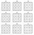
具体的には、まず、視点画像生成部140が、撮像データD0に基づいて複数の視点画像を生成する処理を行う。即ち、図8に示したような撮像データD0に対し、同一の視点方向の画素データ(各ブロック領域U同士の間において互いに同一の位置にある画素から抽出される画素データ)同士を合成する。例えば、撮像データD0の中から全ての画素データ「A」を抽出してこれらを合成する(図9(A))。他の画素データ「B」〜「I」についても同様の処理を行う(図9(B)〜(I))。このようにして、視点画像生成部140は、撮像データD0に基づいて、複数の視点画像(ここでは、第1〜9視点の計9つの視点画像)を生成する。これらの視点画像は、視点画像データD1として、画像合成処理部141へ出力される。
Specifically, first, the viewpoint
上記のような合成処理後の視点画像は、視点画像データD1として、画像補正処理部142へ出力される。画像補正処理部142は、視点画像データD1に対し、例えばデモザイク処理等のカラー補間処理やホワイトバランス調整処理、ガンマ補正処理等を施し、それらの画像処理後の視点画像データを画像データDoutとして出力する。この画像データDoutは、撮像装置1の外部へ出力されるようにしてもよいし、撮像装置1の内部に設けられた記憶部(図示せず)に記憶するようにしてもよい。
The viewpoint image after the synthesis process as described above is output to the image
但し、上記画像データDoutは、視点画像に対応するデータであってもよいし、視点画像生成前の撮像データD0であってもよい。即ち、上記のような視点画像生成処理(抽出して合成する画素データの並べ替え処理)を行わずに、イメージセンサ13から読み出されたデータ配列のままの撮像データD0を外部へ出力するか、あるいは記憶部に記憶するようにしてもよい。
However, the image data Dout may be data corresponding to the viewpoint image, or may be the imaging data D0 before generating the viewpoint image. That is, whether the imaging data D0 that has been read from the
ここで、図10(A)〜(I)に、図9(A)〜(I)に示したデータ配列に対応する視点画像の一具体例(視点画像R1〜R9)を示す。被写体2の画像としては、奥行き方向において互いに異なる位置に配置された3つの被写体「人」,「山」,「花」の画像Ra,Rb,Rcを示している。視点画像R1〜R9は、上記3つの被写体のうち「人」に撮像レンズの焦点が合うようにして撮影されたものであり、「人」よりも奥にある「山」の画像Rbと、「人」よりも手前にある「花」の画像Rcとについてはデフォーカスした画像となっている。撮像装置1では、フォーカスした「人」の画像Raは、視点が変わってもシフトしないが、デフォーカスした画像Rb,Rcは、視点毎に互いに異なる位置にシフトする。尚、図10(A)〜(I)では、各視点画像間の位置シフト(画像Rb,Rcの位置シフト)を誇張して示している。
Here, FIGS. 10A to 10I show specific examples (viewpoint images R1 to R9) of viewpoint images corresponding to the data arrangement shown in FIGS. 9A to 9I. As the image of the subject 2, three images Ra, Rb, and Rc of the subjects “person”, “mountain”, and “flower” arranged at different positions in the depth direction are shown. The viewpoint images R <b> 1 to R <b> 9 were taken so that “person” of the above three subjects is in focus on the imaging lens, and “mountain” image Rb located behind “person” and “ The “flower” image Rc in front of the “person” is a defocused image. In the
上記のような9つの視点画像R1〜R9は、互いに視差を有する多視点画像として様々な用途に利用可能であるが、例えば左視点方向および右視点方向における2つの視点画像を用いて、立体映像表示を行うことができる。この場合、表示される映像の立体感は、それら2つの視点画像間の視差量に応じたものとなる。例えば、図10(D)に示した視点画像R4と、図10(F)に示した視点画像R6とを上記2つの視点画像として用いた場合、表示映像における立体感は、次のようなものとなる。即ち、「山」は「人」よりも奥まって見えるが、その度合いは、図11(A),(B)に示したように、視点画像R4における画像Rb4と視点画像R6における画像Rb6との位置ずれ量(視差量)Wbに応じたものとなる。一方、「花」は「人」よりも手前に飛び出して見えるが、その度合いは、視点画像R4における画像Rc4と視点画像R6における画像Rc6との位置ずれ量Wcに応じたものとなる。そして、位置ずれ量Wb,Wcが大きければ大きい程、「山」はより奥まって、「花」はより飛び出して、それぞれ観察されることとなる。 The nine viewpoint images R1 to R9 as described above can be used for various purposes as multi-viewpoint images having parallax with each other. For example, a stereoscopic video image using two viewpoint images in the left viewpoint direction and the right viewpoint direction is used. Display can be made. In this case, the stereoscopic effect of the displayed video is in accordance with the amount of parallax between the two viewpoint images. For example, when the viewpoint image R4 shown in FIG. 10D and the viewpoint image R6 shown in FIG. 10F are used as the two viewpoint images, the stereoscopic effect in the display video is as follows. It becomes. That is, although “mountain” appears to be deeper than “person”, the degree of the difference between the image Rb4 in the viewpoint image R4 and the image Rb6 in the viewpoint image R6, as shown in FIGS. This is in accordance with the positional deviation amount (parallax amount) Wb. On the other hand, “flower” appears to pop out before “people”, and the degree thereof corresponds to the amount of displacement Wc between the image Rc4 in the viewpoint image R4 and the image Rc6 in the viewpoint image R6. As the positional deviation amounts Wb and Wc are larger, the “mountain” becomes deeper and the “flower” protrudes more and is observed.
(レンズアレイ12Aによる作用)
上述のように、撮像装置1では、撮像レンズ11を通過した光線を、レンズアレイ12Aによって、各視点方向に分離しつつイメージセンサ13へ導くことで、イメージセンサ13の各画素Pにおいて各視点方向の光線をそれぞれ受光可能となっている。ここで、上述のような第1レンズ部S1および第2レンズ部S2を有するレンズアレイ12Aを設けることによる作用について、図12と比較しつつ説明する。
(Operation by
As described above, in the
(比較例)
図12は、本実施の形態の比較例として、焦点距離fのマイクロレンズ(マイクロレンズ102)を用いた場合における、イメージセンサ103への入射光線について表したものである。マイクロレンズ102から、マイクロレンズ102の焦点距離fだけ離れた位置にオンチップレンズ1033が設けられており、マイクロレンズ102を通過した光線がオンチップレンズ1033によって集光され、イメージセンサ103のセンサ部1030へ導かれるようになっている。
(Comparative example)
FIG. 12 shows incident light rays to the
このような比較例では、マイクロレンズ102を通過した主光線のうち、イメージセンサ103のブロック領域Uにおける中央画素P0へ入射する主光線(L100)は、マイクロレンズ102の光軸に沿ってセンサ部1030の受光面に垂直に入射する。このため、この中央画素P0では、マイクロレンズ102を通過した主光線L100がほとんどロスなく受光される。
In such a comparative example, the chief ray (L100) incident on the central pixel P0 in the block region U of the
ところが、マイクロレンズ102を通過した後、ブロック領域Uの周辺画素P1へ向けて入射する主光線(L101)は、画素Pに対して斜めに入射するため、センサ部1030に到達する前に、例えば配線層1031などに吸収され(X)、中央画素P0に比べ、受光量が減少する。また、配線層1031に設けられたメタル1031aに吸収されることにより、いわゆる光電効果によって電子が励起される。これが撮像データにおけるノイズ成分となる。このような画素位置に応じた受光むらやノイズ成分の発生は画質劣化の要因となる。
However, since the principal ray (L101) incident on the peripheral pixel P1 in the block region U after passing through the
(本実施の形態)
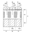
これに対し、本実施の形態では、図13に示したように、レンズアレイ12Aを構成する各マイクロレンズ12A1が、所定の位置関係で配置された第1レンズ部S1および第2レンズS2を有している。これにより、撮像レンズ11および第1レンズ部S1を通過する主光線Lのうち、イメージセンサ13のブロック領域Uにおける中央画素P0へと向かう主光線(L0)は、マイクロレンズ12A1を光軸Z2に沿って通過し、センサ部130の受光面(フォトダイオード130a)に垂直に(略垂直に)入射する。このため、中央画素P0では、マイクロレンズ12A1を通過した主光線L0がロスなくフォトダイオード130aにおいて受光され易い。
(This embodiment)
In contrast, in the present embodiment, as shown in FIG. 13, each micro lens 12A1 constituting the
他方、主光線Lのうち、ブロック領域Uにおける周辺画素P1へ向かう方向へ通過する主光線(L1)は、第2レンズ部S2において、光軸Z2に近づく方向へ向けて屈折される。尚、図示しないが、ブロック領域Uにおいて中央画素と対角線方向において隣接する周辺画素へ向かう主光線についても同様に、第2レンズ部S2において、光軸Z2に近づく方向へ向けて屈折される。これにより、撮像レンズ11および第1レンズ部S1を通過した主光線Lは、各画素Pにおいて受光面130bに略垂直に入射し易くなる。即ち、局所的な領域において光線が配線層130に吸収されるなど、光損失が生じることが低減され、受光量にむらが生じることが抑制される。また、配線層130に吸収される光線が減少することで、光電効果によるノイズの発生が低減される。
On the other hand, the principal ray (L1) passing through the principal ray L in the direction toward the peripheral pixel P1 in the block region U is refracted in the second lens portion S2 toward the direction approaching the optical axis Z2. In addition, although not shown, the principal ray directed toward the peripheral pixel adjacent to the central pixel in the block region U in the diagonal direction is similarly refracted toward the optical axis Z2 in the second lens unit S2. Thereby, the principal ray L that has passed through the
以上のように本実施の形態では、撮像レンズ11、レンズアレイ12Aおよびイメージセンサ13を用いて、視点方向を分離しつつ画像取得を行う撮像装置1において、レンズアレイ12Aとして、第1レンズ部S1と第2レンズ部S2とを所定の位置関係で配置する。このように、レンズアレイ12Aに第2レンズ部S2を設けることで、撮像レンズ11および第1レンズ部S1を通過した主光線を、イメージセンサ13における各画素Pの受光面に略垂直に入射させることができる。これにより、イメージセンサ13では局所的な光損失を低減することができる。よって、レンズアレイ12Aを含む光学系を利用して撮影した画像において、明るさのむらを軽減することが可能となる。
As described above, in the present embodiment, in the
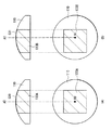
図14(A),(B)に、本実施の形態のレンズアレイ12A(マイクロレンズ12A1)を用いた場合の光線シミュレーションの一例について示す。尚、図14(A)が、本実施の形態に対応する実施例であり、図14(B)は、図12に示した比較例に係るシミュレーション結果である。このように、図14(B)に示した比較例では、受光面1030bへ入射する光線の分布にばらつきが生じているのに対し、図14(A)に示した実施例では、第2レンズ部S2における屈折作用により、受光面130bへ入射する光線の分布にあまりばらつきがみられない。この結果からも、第2レンズ部S2に設けた本実施の形態において、受光量のむらを軽減できることがわかる。
FIGS. 14A and 14B show an example of a ray simulation when the
以下、上記第1の実施の形態の変形例(変形例1,2)について説明する。変形例1,2は、上記第1の実施の形態における撮像装置1において、撮像レンズ11とイメージセンサ13との間に配設されるレンズアレイの他の構成に係るものである。尚、上記実施の形態と同様の構成要素については同一の符号を付し、適宜説明を省略する。
Hereinafter, modified examples (modified examples 1 and 2) of the first embodiment will be described.
<変形例1>
図15は、変形例1に係るレンズアレイ12Bの斜視構成について、イメージセンサ13と共に示したものである。本変形例のレンズアレイ12Bは、上記第1の実施の形態のレンズアレイ12Aと同様、撮像レンズ11(図15には図示せず)側に複数の第1レンズ部S1、イメージセンサ13側に複数の第2レンズ部S2をそれぞれ有し、両者が互いに正対して配置されている。尚、図15においても、簡便化のため、第1レンズ部S1(第2レンズ部S2)をXY方向に3×3の配列で設け、イメージセンサ13としては、そのようなレンズアレイ12Bに対応する9×9の画素からなる領域についてのみ示している。
<
FIG. 15 shows a perspective configuration of a lens array 12 </ b> B according to
但し、本変形例では、レンズアレイ12Bにおいて、第1レンズ部S1と第2レンズ部S2との間が空気層17となっている。即ち、第1レンズ部S1と第2レンズ部S2とが別体として所定の距離(光学的距離は上記第1の実施の形態におけるレンズ間距離と同じ)だけ離隔して配設されている。第1レンズ部S1および第2レンズ部S2の各レンズ形状およびレンズ材料は、上述のように特に限定されるものではないが、ここでは、一例として各レンズ形状が平凸レンズである場合を示している。 However, in this modification, in the lens array 12B, an air layer 17 is formed between the first lens unit S1 and the second lens unit S2. That is, the first lens unit S1 and the second lens unit S2 are separately provided and separated by a predetermined distance (the optical distance is the same as the inter-lens distance in the first embodiment). The lens shapes and lens materials of the first lens portion S1 and the second lens portion S2 are not particularly limited as described above, but here, as an example, a case where each lens shape is a plano-convex lens is shown. Yes.
このような構成においても、第1レンズ部S1は、例えば撮像レンズ11の焦点面に配置され、撮像レンズ11から入射した光線を、複数の視点方向に分離しつつイメージセンサ13へ向かう方向に導くようになっている。第2レンズ部S2は、第1レンズ部S1を通過した主光線を第1レンズ部S1の光軸に近づく方向に向けて屈折させる機能を有する。また詳細には、第1レンズ部S1の主面に第2レンズ部S2の焦点面、第2レンズ部S2の主面に第1レンズ部S1の焦点面がそれぞれ配されるように、第1レンズ部S1および第2レンズ部S2が設けられている。
Even in such a configuration, the first lens unit S1 is disposed, for example, on the focal plane of the
また、このようなレンズアレイ12Bの光出射側には、上記第1の実施の形態と同様、イメージセンサ13が配置され、レンズアレイ12Bを構成する1つのマイクロレンズ(正対する第1レンズ部S1と第2レンズ部S2に相当)には、イメージセンサ13のm×nの画素(ブロック領域U)が割り当てられている。
In addition, as in the first embodiment, the
本変形例のように、レンズアレイ12Bにおいて第1レンズ部S1と第2レンズ部S2とを別体として配置してもよく、このような場合であっても、上記第1の実施の形態と同等の効果を得ることができる。 As in the present modification, the first lens portion S1 and the second lens portion S2 may be arranged separately in the lens array 12B. Even in such a case, the first embodiment is different from the first embodiment. The same effect can be obtained.
<変形例2>
図16は、変形例2に係るレンズアレイ12Aおよびイメージセンサ13の一体化構造を模式的に表したものである。尚、図16では、オンチップレンズの図示を省略している。本変形例では、第1レンズ部S1および第2レンズ部S2を有するレンズアレイ12Aが、イメージセンサ13と一体化して設けられている。即ち、レンズアレイ12Aの第2レンズ部S2とイメージセンサ13とが、図示しないオンチップレンズと樹脂層18を介して積層された構造を有する。このような一体化構造は、イメージセンサ13上に、少なくともオンチップレンズ、樹脂層18、第2レンズ部S2および第1レンズ部S1を積層することにより作製可能である。例えば、イメージセンサ13上に、オンチップレンズ、樹脂層18および第2レンズ部S2を順に形成した後、更に樹脂層を介して第1レンズ部S1を形成することにより一体化構造を作製することができる。あるいは、レンズアレイ12Aを上述したような手法を用いて形成した後、このレンズアレイ12Aを樹脂層18を介してオンチップレンズが形成されたイメージセンサ13上に接着するようにしてもよい。いずれの場合であっても、各層に使用する材料の屈折率を考慮して、第1レンズ部S1および第2レンズ部S2の各レンズ形状を適宜設計すればよい。
<
FIG. 16 schematically shows an integrated structure of the
変形例のように、レンズアレイ12Aをイメージセンサ13およびオンチップレンズと一体的に設けてもよく、このような場合であっても、上記第1の実施の形態と同等の効果を得ることができる。また、レンズアレイ12Aからイメージセンサ13までを一体化構造とすることにより、それぞれの部材同士を位置合わせすることなく、装置内に配設可能となる。また、経時的に部材同士に位置ずれが生じることも抑制され、位置合わせ精度の点においても優れている。
As in the modification, the
<第2の実施の形態>
次に、本発明の第2の実施の形態について説明する。尚、上記第1の実施の形態と同様の構成要素については同一の符号を付し、適宜説明を省略する。
<Second Embodiment>
Next, a second embodiment of the present invention will be described. In addition, the same code | symbol is attached | subjected about the component similar to the said 1st Embodiment, and description is abbreviate | omitted suitably.
[構成]
図17は、第2の実施の形態に係るレンズアレイ12Cの斜視構成について、イメージセンサ13と共に示したものである。本実施の形態のレンズアレイ12Cは、上記第1の実施の形態の第1レンズ部S1に相当するマイクロレンズ12C1を、撮像レンズ11の焦点面に複数有するが、第2レンズ部S2については設けられていない。尚、図17においても、簡便化のため、第1レンズ部S1をXY方向に3×3の配列で設け、イメージセンサ13としては、そのようなレンズアレイ12Bに対応する9×9の画素からなる領域についてのみ示している。本実施の形態では、イメージセンサ13の受光面側に設けられたオンチップレンズ(後述のオンチップレンズ133A〜133C)において、上記第1の実施の形態における第2レンズ部S2と同様の機能を有している。以下、オンチップレンズ133A〜133Cの構成について詳細に説明する。
[Constitution]
FIG. 17 shows a perspective configuration of a lens array 12 </ b> C according to the second embodiment together with the
(オンチップレンズ133A〜133C)
図18は、イメージセンサ13上のオンチップレンズ133A,133Bの断面構成を表したものである。本実施の形態においても、イメージセンサ13上に、上記第1の実施の形態と同様、集光用レンズとして機能するオンチップレンズ133A〜133C(133Cは図18には図示せず)が、画素P毎に設けられている。但し、本実施の形態では、オンチップレンズ133A〜133Cにおける光軸(いわゆる芯)A0〜A2が、画素位置に応じて異なる位置に設けられている。
(On-
FIG. 18 illustrates a cross-sectional configuration of the on-
ブロック領域Uにおいて中央画素P0上に設けられたマイクロレンズ133Aは、XY平面において、光軸A0がレンズ開口形状(XY平面形状)の中心と一致するようなレンズ形状を有している。一方、X方向およびY方向において中央画素P0と隣接する周辺画素P1に配置されたマイクロレンズ133Bでは、光軸A1がレンズ開口形状の中心から内側(中央画素P0に向けて)にシフトしてなるレンズ形状を有している。更に、ブロック領域Uの対角線方向において中央画素P0と隣接する周辺画素P2に配置されたマイクロレンズ133Cでは、光軸A2がレンズの開口形状の中心から内側に向けて、よりシフトしてなるレンズ形状を有している。即ち、中央画素P0(ブロック領域UのXY平面における中心位置)からの距離が大きい程、オンチップレンズは、光軸の位置がより内側へシフトしたようなレンズ形状を有している。
The
尚、このようなオンチップレンズ133A〜133Cは、母体レンズを部分的に切り出した形状を有するが、その際、画素位置に応じて、切り出す領域をシフトさせればよい。即ち、図19(A)に示したように、マイクロレンズ133Aでは、母材レンズ110の中心部分のみを切り出せばよく、図19(B)に示したように、マイクロレンズ133Bでは、母材レンズ110の中心からシフトさせた部分を切り出した形状とすればよい。マイクロレンズ133Cについても同様である。
In addition, although such on-
[作用・効果]
本実施の形態においても、上記第1の実施の形態と同様、図1に示したような撮像レンズ11とイメージセンサ13との間に、レンズアレイ12Cが設けられることにより、撮像レンズ11を通過した光線は、レンズアレイ12Cによって、視点方向毎に分離され、イメージセンサ13の異なる画素において受光される。これにより、イメージセンサ13では、各視点方向からの光線が、互いに異なる画素において受光され、撮像データD0が取得される。このような撮像データD0に対し、上述のような画像処理が施されることにより、複数の視点画像が得られる。
[Action / Effect]
Also in the present embodiment, similarly to the first embodiment, the lens array 12C is provided between the
但し、本実施の形態では、図20に示したように、撮像レンズ11およびマイクロレンズ12C1を通過した主光線Lのうち、イメージセンサ13のブロック領域Uにおける中央画素P0へ向かう主光線L0は、オンチップレンズ133Aを光軸Z2に沿って通過し、センサ部130の受光面130b(フォトダイオード130a)に垂直に(略垂直に)入射する。このため、中央画素P0では、マイクロレンズ12C1を通過した主光線L0がロスなくフォトダイオード130aにおいて受光され易い。
However, in the present embodiment, as shown in FIG. 20, among the principal rays L that have passed through the
他方、主光線Lのうち、周辺画素P1へ向かう方向へ通過した主光線(L1)は、その周辺画素P1上に設けられたオンチップレンズ133Bにおいて、光軸Z2に近づく方向へ向けて屈折される。尚、図20には図示しないが、周辺画素P2へ向かう方向へ通過した主光線は、その周辺画素P2上に設けられたオンチップレンズ133Cにおいて、光軸Z2に近づく方向へ向けて屈折される。これにより、撮像レンズ11およびマイクロレンズ12C1を通過した主光線Lは、各画素Pにおいて受光面130bに略垂直に入射し易くなる。即ち、受光量にむらが生じることが抑制され、また、配線層130に吸収される光線が減少することで、光電効果によるノイズの発生が低減される。
On the other hand, of the principal rays L, the principal ray (L1) that has passed in the direction toward the peripheral pixel P1 is refracted toward the optical axis Z2 in the on-
以上のように本実施の形態では、撮像レンズ11、レンズアレイ12Cおよびイメージセンサ13を用いて、視点方向を分離しつつ画像取得を行う場合、イメージセンサ13のレンズアレイ12C側に、画素位置に応じて光軸がシフトしたレンズ形状を有するオンチップレンズ133A〜133Cを配置する。これにより、撮像レンズ11およびレンズアレイ12Cを通過した主光線を、イメージセンサ13における各画素Pの受光面に略垂直に入射させることができる。よって、上記第1の実施の形態と同等の効果を得ることができる。
As described above, in the present embodiment, when the
以下、上記第2の実施の形態の変形例(変形例3)について説明する。変形例3は、上記第2実施の形態における撮像装置1において、イメージセンサ13上に配設されるオンチップレンズの他の構成に係るものである。尚、上記実施の形態と同様の構成要素については同一の符号を付し、適宜説明を省略する。
Hereinafter, a modification (modification 3) of the second embodiment will be described. The third modification relates to another configuration of the on-chip lens disposed on the
<変形例3>
上記第2の実施の形態では、3×3の画素からなるブロック領域Uにマイクロレンズ12C1が割り当てられた場合を例に挙げたが、割り当て画素数がそれよりも増えた場合であっても上記第2の実施の形態と同様、ブロック領域Uにおける画素位置に応じて、オンチップレンズの光軸を内側にシフトしていればよい。図21に、その一例として5×5の画素を割り当てた場合の一部のマイクロレンズ(133A,133B,133D)について示す。このように、割り当て画素数が増えた場合であっても、同心円状に各オンチップレンズの光軸が配置されるように構成すればよい。
<Modification 3>
In the second embodiment, the case where the microlens 12C1 is assigned to the block region U composed of 3 × 3 pixels is taken as an example. However, even when the number of assigned pixels is increased, the above-described case is described. Similar to the second embodiment, the optical axis of the on-chip lens may be shifted inward according to the pixel position in the block region U. FIG. 21 shows some microlenses (133A, 133B, 133D) when 5 × 5 pixels are allocated as an example. In this way, even when the number of assigned pixels is increased, the optical axes of the on-chip lenses may be arranged concentrically.
<変形例4>
上記第1および第2の実施の形態では、イメージセンサ13として、表面照射型のものを例に挙げて説明したが、イメージセンサ13は、いわゆる裏面照射型であってもよい。図22にその一例を示す。このような裏面照射型のイメージセンサ13では、フォトダイオード130aを含むセンサ部130の光入射側と反対側に配線層131が設けられるため、オンチップレンズ133を通過した光線を配線層131を介さずに、センサ部130において受光することができる。このため、表面照射型に比べ受光感度が高く、約2倍程度の明るさを実現できる。
<Modification 4>
In the first and second embodiments, the front side illumination
以上、実施の形態および変形例を挙げて本発明を説明したが、本発明は上記実施の形態に限定されるものではなく、種々の変形が可能である。例えば、上記実施の形態では、レンズ割り当て画素(画素領域)m×n=3×3である場合を例に挙げて説明したが、各レンズに割り当てられる画素領域は、これに限定されず、例えばm,nが2または4以上であってもよいし、m,nが互いに異なっていてもよい。 Although the present invention has been described with reference to the embodiment and the modifications, the present invention is not limited to the above embodiment, and various modifications can be made. For example, in the above-described embodiment, the case where the lens allocation pixel (pixel area) m × n = 3 × 3 is described as an example. However, the pixel area allocated to each lens is not limited to this. For example, m and n may be 2 or 4 or more, and m and n may be different from each other.
更に、上記実施の形態等では、本発明の撮像装置の一例として、視点画像を生成する画像処理部を備えたものを例に挙げて説明したが、この画像処理部については必ずしも備えていなくともよい。 Furthermore, in the above-described embodiment and the like, as an example of the imaging apparatus of the present invention, an example including an image processing unit that generates a viewpoint image has been described as an example. However, this image processing unit is not necessarily provided. Good.
1…撮像装置、11…撮像レンズ、12A,12B,12C…レンズアレイ、12A1,12C1…マイクロレンズ、13…イメージセンサ、14…画像処理部、15…イメージセンサ駆動部、16…制御部、133,133A〜133C…オンチップレンズ、140…視点画像生成部、142…画像補正処理部、143…奥行き情報取得部、2…被写体、S1…第1レンズ部、S2…第2レンズ部、D0…撮像データ、D1…視点画像データ、Dout…画像データ、R1〜R9…視点画像。
DESCRIPTION OF
Claims (7)
前記撮像レンズの結像面に設けられたレンズアレイを有する光学系と、
前記撮像レンズおよび前記光学系の通過光線を受光して撮像データを取得する撮像素子とを備え、
前記光学系は、前記レンズアレイを構成する各レンズを通過する主光線を、各レンズの光軸に近づく方向に向けて屈折させるように構成されている
撮像装置。 An imaging lens;
An optical system having a lens array provided on the imaging surface of the imaging lens;
An imaging device that receives the passing light of the imaging lens and the optical system and acquires imaging data;
The optical system is configured to refract chief rays passing through each lens constituting the lens array in a direction approaching an optical axis of each lens.
前記撮像レンズの結像面に配置された複数の第1レンズ部と、
それぞれが、各第1レンズ部と正対すると共に、前記第1レンズ部を通過した主光線を前記光軸に近づく方向に向けて屈折させる複数の第2レンズ部と
を有する請求項1に記載の撮像装置。 The lens array is
A plurality of first lens portions disposed on an imaging surface of the imaging lens;
2. Each of the plurality of second lens units facing each first lens unit and refracting a principal ray that has passed through the first lens unit in a direction approaching the optical axis. Imaging device.
請求項2に記載の撮像装置。 The first lens unit and the main surface of the second lens unit are arranged on the focal plane of the first lens unit, and the main surface of the first lens unit is arranged on the focal plane of the second lens unit. The imaging device according to claim 2, wherein a second lens unit is provided.
請求項3に記載の撮像装置。 The imaging device according to claim 3, wherein the plurality of first lens portions and the plurality of second lens portions are integrated in the lens array.
請求項4に記載の撮像装置。 The imaging device according to claim 4, wherein the lens array and the imaging element are provided integrally.
前記光学系として、前記レンズアレイと、前記撮像素子の前記レンズアレイ側に、それぞれが画素毎に配置されると共に、集光機能を有する複数の第3レンズ部とを有し、
前記複数の第3レンズ部が、前記レンズアレイの各レンズを通過した主光線を前記光軸に近づく方向に向けて屈折させる
請求項1に記載の撮像装置。 The imaging element includes a plurality of pixels arranged two-dimensionally,
As the optical system, the lens array, and a plurality of third lens portions that are arranged for each pixel on the lens array side of the image sensor and have a light collecting function,
The imaging device according to claim 1, wherein the plurality of third lens units refract chief rays that have passed through the lenses of the lens array in a direction approaching the optical axis.
前記複数の第3レンズ部はそれぞれ、前記ブロック領域における画素位置に応じて異なる位置に光軸を有する
請求項6に記載の撮像装置。 Each lens in the lens array is arranged opposite to a block region of m × n (m, n is an integer of 1 or more, except for m = n = 1) among the plurality of pixels.
The imaging device according to claim 6, wherein each of the plurality of third lens units has an optical axis at a different position according to a pixel position in the block region.
Priority Applications (3)
| Application Number | Priority Date | Filing Date | Title |
|---|---|---|---|
| JP2011052002A JP5716465B2 (en) | 2011-03-09 | 2011-03-09 | Imaging device |
| CN201210059254.1A CN102685377B (en) | 2011-03-09 | 2012-03-02 | camera device |
| US13/410,438 US9116271B2 (en) | 2011-03-09 | 2012-03-02 | Image pickup apparatus |
Applications Claiming Priority (1)
| Application Number | Priority Date | Filing Date | Title |
|---|---|---|---|
| JP2011052002A JP5716465B2 (en) | 2011-03-09 | 2011-03-09 | Imaging device |
Publications (2)
| Publication Number | Publication Date |
|---|---|
| JP2012189708A true JP2012189708A (en) | 2012-10-04 |
| JP5716465B2 JP5716465B2 (en) | 2015-05-13 |
Family
ID=46795244
Family Applications (1)
| Application Number | Title | Priority Date | Filing Date |
|---|---|---|---|
| JP2011052002A Active JP5716465B2 (en) | 2011-03-09 | 2011-03-09 | Imaging device |
Country Status (3)
| Country | Link |
|---|---|
| US (1) | US9116271B2 (en) |
| JP (1) | JP5716465B2 (en) |
| CN (1) | CN102685377B (en) |
Cited By (8)
| Publication number | Priority date | Publication date | Assignee | Title |
|---|---|---|---|---|
| JP2014119702A (en) * | 2012-12-19 | 2014-06-30 | Casio Comput Co Ltd | Microlens array, light intensity distribution uniformization element having the same provided and projection device having light intensity distribution uniformization element |
| JP2014154755A (en) * | 2013-02-12 | 2014-08-25 | Canon Inc | Imaging device having imaging element with pupil division means for photographic lens, and manufacturing method for imaging element |
| JP2016158154A (en) * | 2015-02-25 | 2016-09-01 | 株式会社リコー | Photoelectric conversion element, image reading device, and image forming apparatus |
| JP2017046296A (en) * | 2015-08-28 | 2017-03-02 | 大日本印刷株式会社 | Imaging module, imaging device |
| WO2017056865A1 (en) * | 2015-09-29 | 2017-04-06 | 大日本印刷株式会社 | Lens sheet, lens sheet unit, imaging module, imaging device |
| WO2017150512A1 (en) * | 2016-03-01 | 2017-09-08 | 三菱電機株式会社 | Image reading device |
| KR20210105416A (en) * | 2019-01-25 | 2021-08-26 | 에이에스엠엘 네델란즈 비.브이. | Wavefront sensors and associated metrology devices |
| JP2023091707A (en) * | 2021-12-20 | 2023-06-30 | 采▲ぎょく▼科技股▲ふん▼有限公司 | Image processing method and image processing system |
Families Citing this family (19)
| Publication number | Priority date | Publication date | Assignee | Title |
|---|---|---|---|---|
| JP5699609B2 (en) | 2011-01-06 | 2015-04-15 | ソニー株式会社 | Image processing apparatus and image processing method |
| JP5710835B2 (en) * | 2012-03-21 | 2015-04-30 | 富士フイルム株式会社 | Imaging device |
| US20140077324A1 (en) * | 2012-09-20 | 2014-03-20 | Sony Corporation | Solid-state image pickup device, method of manufacturing solid-state image pickup device, and electronic apparatus |
| US9398264B2 (en) | 2012-10-19 | 2016-07-19 | Qualcomm Incorporated | Multi-camera system using folded optics |
| US9077879B2 (en) * | 2013-01-09 | 2015-07-07 | Aac Acoustic Technologies (Shenzhen) Co., Ltd. | Array camera |
| US10178373B2 (en) | 2013-08-16 | 2019-01-08 | Qualcomm Incorporated | Stereo yaw correction using autofocus feedback |
| US9383550B2 (en) | 2014-04-04 | 2016-07-05 | Qualcomm Incorporated | Auto-focus in low-profile folded optics multi-camera system |
| US9374516B2 (en) | 2014-04-04 | 2016-06-21 | Qualcomm Incorporated | Auto-focus in low-profile folded optics multi-camera system |
| US10013764B2 (en) | 2014-06-19 | 2018-07-03 | Qualcomm Incorporated | Local adaptive histogram equalization |
| US9541740B2 (en) | 2014-06-20 | 2017-01-10 | Qualcomm Incorporated | Folded optic array camera using refractive prisms |
| US9386222B2 (en) | 2014-06-20 | 2016-07-05 | Qualcomm Incorporated | Multi-camera system using folded optics free from parallax artifacts |
| US9294672B2 (en) | 2014-06-20 | 2016-03-22 | Qualcomm Incorporated | Multi-camera system using folded optics free from parallax and tilt artifacts |
| US9819863B2 (en) | 2014-06-20 | 2017-11-14 | Qualcomm Incorporated | Wide field of view array camera for hemispheric and spherical imaging |
| CN104486555B (en) | 2014-10-28 | 2019-02-12 | 北京智谷睿拓技术服务有限公司 | Image acquisition control method and device |
| US9832381B2 (en) | 2014-10-31 | 2017-11-28 | Qualcomm Incorporated | Optical image stabilization for thin cameras |
| US20170038502A1 (en) * | 2015-08-06 | 2017-02-09 | Qualcomm Incorporated | Methods and apparatus having a two-surface microlens array for low f-number plenoptic cameras |
| CN105590939B (en) * | 2015-12-18 | 2019-07-19 | Oppo广东移动通信有限公司 | Image sensor, output method, phase focusing method, imaging device and terminal |
| GB2576212B (en) * | 2018-08-10 | 2021-12-29 | X Fab Semiconductor Foundries Gmbh | Improvements in lens layers for semiconductor devices |
| CN112099113B (en) * | 2020-09-25 | 2021-09-21 | 清华大学 | Super-surface micro-lens array for image sensor |
Citations (2)
| Publication number | Priority date | Publication date | Assignee | Title |
|---|---|---|---|---|
| JP2007004471A (en) * | 2005-06-23 | 2007-01-11 | Nikon Corp | Image composition method and imaging apparatus |
| JP2010057067A (en) * | 2008-08-29 | 2010-03-11 | Sony Corp | Image pickup apparatus and image processing apparatus |
Family Cites Families (7)
| Publication number | Priority date | Publication date | Assignee | Title |
|---|---|---|---|---|
| US20040223071A1 (en) | 2003-05-08 | 2004-11-11 | David Wells | Multiple microlens system for image sensors or display units |
| JP3729353B2 (en) | 2003-06-18 | 2005-12-21 | 松下電器産業株式会社 | Solid-state imaging device and manufacturing method thereof |
| US20060131683A1 (en) | 2004-12-17 | 2006-06-22 | Eastman Kodak Company | Microlens array |
| JP4334495B2 (en) * | 2005-03-29 | 2009-09-30 | 株式会社東芝 | Stereoscopic image display device |
| US7470556B2 (en) | 2005-06-28 | 2008-12-30 | Aptina Imaging Corporation | Process for creating tilted microlens |
| KR100821480B1 (en) | 2006-12-22 | 2008-04-11 | 동부일렉트로닉스 주식회사 | Image sensor and manufacturing method thereof |
| US8400555B1 (en) * | 2009-12-01 | 2013-03-19 | Adobe Systems Incorporated | Focused plenoptic camera employing microlenses with different focal lengths |
-
2011
- 2011-03-09 JP JP2011052002A patent/JP5716465B2/en active Active
-
2012
- 2012-03-02 US US13/410,438 patent/US9116271B2/en active Active
- 2012-03-02 CN CN201210059254.1A patent/CN102685377B/en not_active Expired - Fee Related
Patent Citations (2)
| Publication number | Priority date | Publication date | Assignee | Title |
|---|---|---|---|---|
| JP2007004471A (en) * | 2005-06-23 | 2007-01-11 | Nikon Corp | Image composition method and imaging apparatus |
| JP2010057067A (en) * | 2008-08-29 | 2010-03-11 | Sony Corp | Image pickup apparatus and image processing apparatus |
Cited By (15)
| Publication number | Priority date | Publication date | Assignee | Title |
|---|---|---|---|---|
| US9500797B2 (en) | 2012-12-19 | 2016-11-22 | Casio Computer Co., Ltd. | Microlens array, light intensity distribution uniformizing element having same, and projection apparatus having light intensity distribution uniformizing element |
| JP2014119702A (en) * | 2012-12-19 | 2014-06-30 | Casio Comput Co Ltd | Microlens array, light intensity distribution uniformization element having the same provided and projection device having light intensity distribution uniformization element |
| JP2014154755A (en) * | 2013-02-12 | 2014-08-25 | Canon Inc | Imaging device having imaging element with pupil division means for photographic lens, and manufacturing method for imaging element |
| JP2016158154A (en) * | 2015-02-25 | 2016-09-01 | 株式会社リコー | Photoelectric conversion element, image reading device, and image forming apparatus |
| JP2017046296A (en) * | 2015-08-28 | 2017-03-02 | 大日本印刷株式会社 | Imaging module, imaging device |
| US11333802B2 (en) | 2015-09-29 | 2022-05-17 | Dai Nippon Printing Co., Ltd. | Lens sheet, lens sheet unit, imaging module, imaging device |
| WO2017056865A1 (en) * | 2015-09-29 | 2017-04-06 | 大日本印刷株式会社 | Lens sheet, lens sheet unit, imaging module, imaging device |
| WO2017150512A1 (en) * | 2016-03-01 | 2017-09-08 | 三菱電機株式会社 | Image reading device |
| US10270944B2 (en) | 2016-03-01 | 2019-04-23 | Mitsubishi Electric Corporation | Image capturing device |
| JPWO2017150512A1 (en) * | 2016-03-01 | 2018-06-28 | 三菱電機株式会社 | Image reading device |
| KR20210105416A (en) * | 2019-01-25 | 2021-08-26 | 에이에스엠엘 네델란즈 비.브이. | Wavefront sensors and associated metrology devices |
| KR102770084B1 (en) | 2019-01-25 | 2025-02-18 | 에이에스엠엘 네델란즈 비.브이. | Wavefront sensors and associated measuring devices |
| JP2023091707A (en) * | 2021-12-20 | 2023-06-30 | 采▲ぎょく▼科技股▲ふん▼有限公司 | Image processing method and image processing system |
| US11832001B2 (en) | 2021-12-20 | 2023-11-28 | Visera Technologies Company Limited | Image processing method and image processing system |
| JP7429731B2 (en) | 2021-12-20 | 2024-02-08 | 采▲ぎょく▼科技股▲ふん▼有限公司 | Image processing method and image processing system |
Also Published As
| Publication number | Publication date |
|---|---|
| CN102685377B (en) | 2017-03-01 |
| JP5716465B2 (en) | 2015-05-13 |
| CN102685377A (en) | 2012-09-19 |
| US9116271B2 (en) | 2015-08-25 |
| US20120229688A1 (en) | 2012-09-13 |
Similar Documents
| Publication | Publication Date | Title |
|---|---|---|
| JP5716465B2 (en) | Imaging device | |
| JP5672989B2 (en) | Imaging device | |
| CN103229498B (en) | Photographing element and camera device | |
| JP5421207B2 (en) | Solid-state imaging device | |
| JP5454424B2 (en) | Imaging method | |
| JP5515396B2 (en) | Imaging device | |
| JP5214754B2 (en) | Solid-state imaging device and portable information terminal | |
| CN102227811B (en) | Solid-state image pickup device and image pickup apparatus | |
| JP2015230355A (en) | Imaging device and image pickup element | |
| JP2014164174A (en) | Solid-state image pickup device, portable information terminal and solid-state imaging system | |
| CN103828346B (en) | Solid camera head | |
| JP2012191351A (en) | Image pickup apparatus and image processing method | |
| CN104106003A (en) | Imaging device | |
| JP2020178120A (en) | Image sensor and image sensor | |
| CN103503447B (en) | The control method of filming apparatus and filming apparatus | |
| JP6089440B2 (en) | Imaging device and imaging apparatus | |
| JP5907668B2 (en) | Imaging device and imaging device | |
| JP5568150B2 (en) | Solid-state imaging device and portable information terminal | |
| JP5537687B2 (en) | Solid-state imaging device | |
| JP6476630B2 (en) | Imaging device | |
| JP6323493B2 (en) | Imaging device and imaging apparatus | |
| JP6051570B2 (en) | Imaging device and imaging apparatus | |
| JP5991461B2 (en) | Imaging apparatus and imaging program thereof | |
| WO2020213610A1 (en) | Image capturing element and image capturing device | |
| JP2018137457A (en) | Imaging device and imaging apparatus |
Legal Events
| Date | Code | Title | Description |
|---|---|---|---|
| A621 | Written request for application examination |
Free format text: JAPANESE INTERMEDIATE CODE: A621 Effective date: 20140224 |
|
| A977 | Report on retrieval |
Free format text: JAPANESE INTERMEDIATE CODE: A971007 Effective date: 20141126 |
|
| A131 | Notification of reasons for refusal |
Free format text: JAPANESE INTERMEDIATE CODE: A131 Effective date: 20141203 |
|
| A521 | Request for written amendment filed |
Free format text: JAPANESE INTERMEDIATE CODE: A523 Effective date: 20150126 |
|
| TRDD | Decision of grant or rejection written | ||
| A01 | Written decision to grant a patent or to grant a registration (utility model) |
Free format text: JAPANESE INTERMEDIATE CODE: A01 Effective date: 20150217 |
|
| A61 | First payment of annual fees (during grant procedure) |
Free format text: JAPANESE INTERMEDIATE CODE: A61 Effective date: 20150302 |
|
| R151 | Written notification of patent or utility model registration |
Ref document number: 5716465 Country of ref document: JP Free format text: JAPANESE INTERMEDIATE CODE: R151 |
|
| R250 | Receipt of annual fees |
Free format text: JAPANESE INTERMEDIATE CODE: R250 |
|
| R250 | Receipt of annual fees |
Free format text: JAPANESE INTERMEDIATE CODE: R250 |
|
| R250 | Receipt of annual fees |
Free format text: JAPANESE INTERMEDIATE CODE: R250 |