JP2012190145A - Semiconductor integrated circuit - Google Patents
Semiconductor integrated circuit Download PDFInfo
- Publication number
- JP2012190145A JP2012190145A JP2011051676A JP2011051676A JP2012190145A JP 2012190145 A JP2012190145 A JP 2012190145A JP 2011051676 A JP2011051676 A JP 2011051676A JP 2011051676 A JP2011051676 A JP 2011051676A JP 2012190145 A JP2012190145 A JP 2012190145A
- Authority
- JP
- Japan
- Prior art keywords
- signal
- power supply
- circuit
- supply voltage
- level
- Prior art date
- Legal status (The legal status is an assumption and is not a legal conclusion. Google has not performed a legal analysis and makes no representation as to the accuracy of the status listed.)
- Withdrawn
Links
Images



Landscapes
- Power Sources (AREA)
- Direct Current Feeding And Distribution (AREA)
- Logic Circuits (AREA)
Abstract
【課題】コンデンサの供給する電源電圧の低下により、誤動作を起こす虞がある。
【解決手段】通常動作より低い消費電力状態である低消費電力モードを有する半導体集積回路であって、前記低消費電力モード状態時に、電源電圧レベルを検出する検出手段と、前記検出した電源電圧レベルを記憶する記憶手段と、前記通常動作時よりも小さい電流を流すことで、前記電源電圧を低下させる擬似負荷手段と、前記擬似負荷手段により電流を流す前に前記記憶手段で記憶した第1の電圧レベルに応じて前記検出手段の検出レベルを第2の電圧レベルに切り換える切換え手段と、前記擬似負荷手段により電流を流すことにより低下した前記電源電圧が、前記第2の電圧レベルとなるかを判定し、前記低消費電力モードを解除するか否かの制御を行う制御手段と、を有する半導体集積回路。
【選択図】図1There is a risk of malfunction due to a decrease in power supply voltage supplied by a capacitor.
A semiconductor integrated circuit having a low power consumption mode that is in a power consumption state lower than a normal operation, wherein the power supply voltage level is detected in the low power consumption mode state, and the detected power supply voltage level Storage means for storing, a pseudo load means for lowering the power supply voltage by flowing a current smaller than that during the normal operation, and a first stored in the storage means before flowing current through the pseudo load means A switching means for switching the detection level of the detection means to a second voltage level according to a voltage level, and whether the power supply voltage lowered by flowing a current through the pseudo load means becomes the second voltage level. Control means for determining and controlling whether or not to release the low power consumption mode.
[Selection] Figure 1
Description
本発明は、半導体集積回路に関するものである。 The present invention relates to a semiconductor integrated circuit.
リモコン等の電池駆動装置に搭載される半導体集積回路(以降、LSIと称す)の分野においては、電池駆動装置の設定データが消失しないように、電池が抜かれたときはLSIの電源電圧には外付けコンデンサからチャージされた電圧が供給されるようになっている。通常、リモコンには使用者に合わせた設定データがRAMに保持されており、この設定データが消失すると、改めてデータを設定する必要性が生じる。 In the field of semiconductor integrated circuits (hereinafter referred to as LSI) mounted on battery drive devices such as remote controls, the power supply voltage of the LSI is external when the battery is removed so that the setting data of the battery drive device is not lost. The voltage charged from the attached capacitor is supplied. Normally, the remote controller holds setting data suitable for the user in the RAM, and if this setting data is lost, it becomes necessary to set the data again.
電池を抜かれ、外付けのコンデンサからチャージされた電圧により電源電圧を供給している場合において、大電流が発生して電源電圧が下がると保持している設定データが消失する虞がある。このため、LSIは、設定データを消失しないように、CPUの動作、および、ウォッチドックタイマ用の低周波クロック以外の周辺回路のクロックが停止している低消費電力状態(以降、STOP状態と称す)になっている。 In the case where the power supply voltage is supplied by the voltage charged from the external capacitor when the battery is removed, there is a possibility that the stored setting data may be lost if a large current is generated and the power supply voltage is lowered. Therefore, the LSI operates in a low power consumption state (hereinafter referred to as a STOP state) in which the operation of the CPU and the clocks of peripheral circuits other than the low-frequency clock for the watchdog timer are stopped so as not to lose the setting data. )It has become.
しかし、電池を抜いたときに、誤ってSTOP状態解除キーが押されると、STOP状態が解除され、CPU及び周辺回路が動作する。CPU及び周辺回路が動作状態になることで大電流が流れ、コンデンサにより供給されている電源電圧は急激に低下する。そして、電源電圧がLSIの最低動作電圧以下となってしまい、周辺回路が誤動作してRAMの値が書き換えられてしまう事態や、RAMがデータを保持する限界電圧(以降、RAM保持電圧と称す)まで電源電圧が低下することで、RAMに設定されたデータが消失する虞がある。 However, if the STOP state release key is accidentally pressed when the battery is removed, the STOP state is released and the CPU and peripheral circuits operate. When the CPU and peripheral circuits are in an operating state, a large current flows, and the power supply voltage supplied by the capacitor rapidly decreases. Then, the power supply voltage becomes lower than the minimum operating voltage of the LSI, the peripheral circuit malfunctions and the value of the RAM is rewritten, or the limit voltage at which the RAM holds data (hereinafter referred to as the RAM holding voltage). If the power supply voltage is lowered to the maximum, the data set in the RAM may be lost.
このような理由で、電池を抜かれて外付けのコンデンサにチャージされた電圧によりLSIの電源電圧を供給するSTOP状態のような低消費電力状態を継続させる要求(必要性)が高まってきた。 For this reason, there has been an increasing demand (necessity) for continuing a low power consumption state such as a STOP state in which the power supply voltage of the LSI is supplied by the voltage charged to the external capacitor after the battery is removed.
低消費電力状態を継続させる従来技術として特許文献1のようなものがある。特許文献1には、レジューム機能(電源を切る直前の状態をメモリへ一時的に保存し、再度電源を入れたときすぐに作業を再開できる機能)のついたコンピュータシステムにおいて、省電力のためにサスペンド状態(データやプログラムを作業時の状態のままにして動作を一時的に停止している状態)から擬似負荷で電流を流し、バッテリ電圧が閾値を下回った場合はレジューム動作を中止しサスペンド状態を維持する技術が開示されている。
There exists a thing like
図9に、特許文献1に記載されているコンピュータシステム10のブロック回路図を示す。図9に示すように、コンピュータシステム10は、論理回路12と、トランジスタTと、電圧検出器20とを有する。
FIG. 9 is a block circuit diagram of the
論理回路12には、入力端子16を介してオペレータからのレジューム要求信号aが入力され、電圧検出器20からハイレベルまたはロウレベルの電圧検出信号bが与えられ、そして論理回路12からはトランジスタTをオン/オフさせるための制御信号が出力される。電圧検出器20には、バッテリ18が接続され、電圧検出器20からは、バッテリ18の電圧値が電圧検出器20の閾値より大きいときハイレベル信号が、バッテリ18の電圧値が閾値よりも小さいときロウレベル信号が出力される。
The
トランジスタTについては、エミッタが接地され、ベースが抵抗R1を介して接地されるとともに抵抗R2を介して論理回路12と接続され、そしてコレクタが抵抗R3を介してバッテリ18および電源回路22に接続される。なお、電圧検出器20の閾値は、レジューム時に必要な電流がバッテリ18から取り出されたとき電源回路22が電源電圧Vccを安定して供給できる最小のバッテリ電圧値に設定される。
For transistor T, the emitter is grounded, the base is grounded via resistor R1 and connected to
また、論理回路14(図9中不図示)には論理回路12の出力信号hおよび電圧検出信号bが入力され、これらの信号に基づいて処理された信号jが、レジューム信号として出力端子24から出力される。
The logic circuit 14 (not shown in FIG. 9) receives the output signal h and the voltage detection signal b of the
コンピュータシステム10は、入力端子16にレジューム要求aが与えられると、トランジスタTにハイレベルが与えられ、トランジスタTが導通する。バッテリ(電池)電圧が所定以下のときには、電圧検出器20からの電圧検出信号bはロウレベルになるため、レジューム信号hが出力せず、レジューム動作が中止される。
In the
このように、特許文献1のコンピュータシステムは、バッテリ(電池)で駆動され、かつレジューム機能を有するコンピュータシステムにおいて、サスペンド状態のときにレジューム要求を入力する入力手段、バッテリの出力電圧を閾値と比較する比較手段、レジューム要求が入力されたとき、出力電圧が閾値以上であれば擬似負荷を前記バッテリに接続し、出力電圧が閾値を下回っていれば擬似負荷のバッテリへの接続を禁止する接続制御手段、および擬似負荷がバッテリに接続されたとき、出力電圧が閾値以上であればレジュームを実行し、出力電圧が閾値を下回ればサスペンド状態を継続するレジューム制御手段を備えることを特徴とする。
As described above, the computer system of
しかし、上述した従来技術は、電源電圧を電圧検出器の閾値でしか判別せず、電源電圧が電圧検出器の閾値を下回る場合は動作を停止するが、閾値を上回る場合は動作許可される構成のため、電源電圧が電池で供給されているか、コンデンサで供給されているかを判別出来ない。 However, the above-described conventional technology only determines the power supply voltage based on the threshold value of the voltage detector, and stops the operation when the power supply voltage falls below the threshold value of the voltage detector, but permits the operation when the power supply voltage exceeds the threshold value. Therefore, it cannot be determined whether the power supply voltage is supplied by a battery or a capacitor.
このため、従来技術をリモコンに適用し、電池が抜かれて電源電圧の供給がコンデンサとなった場合、リモコンの電源に接続されるコンデンサは47μF程度であるので、電圧検出器の閾値を上回ることで動作許可されると、CPU及び周辺回路が動作状態になる。このことにより、LSIに大電流が流れ、コンデンサにより供給される電源電圧は急激に低下し、LSIの最低動作電圧以下となり、LSIの周辺回路が誤動作してRAMの値が書き換えられてしまう問題が起きる。 For this reason, when the conventional technology is applied to the remote control and the battery is removed and the supply of power supply voltage becomes a capacitor, the capacitor connected to the power supply of the remote control is about 47 μF, and thus exceeds the threshold of the voltage detector. When the operation is permitted, the CPU and peripheral circuits are in an operating state. As a result, a large current flows through the LSI, and the power supply voltage supplied by the capacitor drops sharply, becomes lower than the minimum operating voltage of the LSI, and the LSI peripheral circuit malfunctions and the RAM value is rewritten. Get up.
また、RAM保持電圧以下に電源電圧が低下することでRAMに設定されたデータが消失してしまう問題が起きる。 Further, when the power supply voltage is lowered below the RAM holding voltage, there is a problem that data set in the RAM is lost.
これは、リモコンの動作状態では、電圧検出回路により電圧降下を検出させパワーオンクリア(以降、POCと称す)を出力させ、リセットをかけて動作停止させようとしても、赤外線LEDが点灯することでピークの消費電流が0.5A〜1A程度となり、POC出力する前に、電源電圧が急激に低下し最低動作電圧以下となり誤動作してしまうからである。 This is because in the operating state of the remote control, the voltage detection circuit detects a voltage drop, outputs a power-on clear (hereinafter referred to as POC), and resets to stop the operation, so that the infrared LED is lit. This is because the peak current consumption is about 0.5 A to 1 A, and before the POC is output, the power supply voltage rapidly decreases and becomes lower than the minimum operating voltage, resulting in malfunction.
ここで、最低動作電圧とPOC電圧とRAM保持電圧の電圧レベルの関係について記述する。電圧の関係は「POC電圧>最低動作電圧>RAM保持電圧」になり、最低動作電圧に到達する前にPOC発生によりリセットをかけ動作を停止させ、RAMの値が保持し、正常動作する限界が最低動作電圧であるため、前述の関係になっている。 Here, the relationship among the minimum operating voltage, the POC voltage, and the voltage level of the RAM holding voltage will be described. The voltage relationship is “POC voltage> minimum operating voltage> RAM holding voltage”. Before reaching the minimum operating voltage, a reset is generated by POC generation to stop the operation, the RAM value is held, and there is a limit to normal operation Since it is the minimum operating voltage, the above-described relationship is established.
具体的な数値を用いて動作説明する。LSIの最低動作電圧が1.4V、RAM保持電圧が0.9V、POC電圧2.0V、動作停止するための電圧検出回路の閾値電圧を2.1V、擬似負荷5Ω(400mA)、擬似負荷のON時間100μS、電池が抜かれて47μFのコンデンサにて3.2Vの電圧が充電されている状態で計算する。 The operation will be described using specific numerical values. The minimum operating voltage of the LSI is 1.4V, the RAM holding voltage is 0.9V, the POC voltage is 2.0V, the threshold voltage of the voltage detection circuit for stopping the operation is 2.1V, the pseudo load is 5Ω (400 mA), the pseudo load The calculation is performed with the ON time 100 μS, the battery removed, and a voltage of 3.2 V charged with a 47 μF capacitor.
擬似負荷がONする前にコンデンサは3.2Vの電圧が充電されており、擬似負荷5Ω(400mA)、ON時間100μSとしてコンデンサに充電された電圧を計算すると、2.16Vとなり、動作停止する閾値電圧2.1Vより高い電圧のため動作許可される。動作許可により動作開始するが、消費電流によりやがてLSIの電源電圧が低下してPOC出力する事態になる。しかし、POC出力までの反応時間が200μSであるとすると、この間にさらに0.85Vまで低下することになる。よって、LSIの最低動作電圧1.4V、RAM保持電圧0.9Vより低下し、LSIの周辺回路が誤動作してRAMの値が書き換えられてしまう事態や、RAM保持電圧まで電源電圧が低下することでRAMに設定されたデータが消失してしまう事態に陥ってしまう。 Before the pseudo load is turned on, the capacitor is charged with a voltage of 3.2 V, and when the voltage charged in the capacitor is calculated with a pseudo load of 5Ω (400 mA) and an ON time of 100 μS, it becomes 2.16 V. Operation is permitted because the voltage is higher than 2.1V. Although the operation starts when the operation is permitted, the power supply voltage of the LSI is lowered due to the current consumption, and POC is output. However, if the reaction time to the POC output is 200 μS, it will further drop to 0.85 V during this time. Therefore, the minimum operating voltage of the LSI is lower than 1.4V and the RAM holding voltage of 0.9V, the peripheral circuit of the LSI malfunctions and the RAM value is rewritten, and the power supply voltage is lowered to the RAM holding voltage. As a result, the data set in the RAM is lost.
本発明は、通常動作より低い消費電力状態である低消費電力モードを有する半導体集積回路であって、前記低消費電力モード状態時に、電源電圧レベルを検出する検出手段と、前記検出した電源電圧レベルを記憶する記憶手段と、前記通常動作時よりも小さい電流を流すことで、前記電源電圧を低下させる擬似負荷手段と、前記擬似負荷手段により電流を流す前に前記記憶手段で記憶した第1の電圧レベルに応じて前記検出手段の検出レベルを第2の電圧レベルに切り換える切換え手段と、前記擬似負荷手段により電流を流すことにより低下した前記電源電圧が、前記第2の電圧レベルとなるかを判定し、前記低消費電力モードを解除するか否かの制御を行う制御手段と、を有する半導体集積回路である。 The present invention relates to a semiconductor integrated circuit having a low power consumption mode that is in a power consumption state lower than that of a normal operation, the detection means for detecting a power supply voltage level in the low power consumption mode state, and the detected power supply voltage level Storage means for storing, a pseudo load means for lowering the power supply voltage by flowing a current smaller than that during the normal operation, and a first stored in the storage means before flowing current through the pseudo load means A switching means for switching the detection level of the detection means to a second voltage level according to a voltage level, and whether the power supply voltage lowered by flowing a current through the pseudo load means becomes the second voltage level. Control means for determining and controlling whether or not to release the low power consumption mode.
本発明では、擬似負荷手段にて電流を流す前の電源電圧範囲を検出し、検出した電源電圧レベルに応じて検出レベルを低下させるよう変更し、通常動作電流より少ない電流で擬似負荷に電流を流し、電源電圧が上記変更検出レベルまで低下する場合には、例えば電力供給能力が小さいコンデンサ等から電源電圧が供給されていると判断することが可能となる。逆に電源電圧が上記変更検出レベルまで低下しない場合には、十分な電力供給能力を備える電池等が接続されていると判断することが可能となる。 In the present invention, the power supply voltage range before flowing the current is detected by the simulated load means, and the detection level is changed to be lowered according to the detected power supply voltage level, and the current is supplied to the simulated load with a current smaller than the normal operation current. When the power supply voltage drops to the change detection level, it can be determined that the power supply voltage is supplied from, for example, a capacitor having a small power supply capability. Conversely, if the power supply voltage does not drop to the change detection level, it can be determined that a battery or the like having sufficient power supply capability is connected.
本発明は、半導体集積回路の電源電圧を電力供給能力が小さいコンデンサ等のから供給する場合に、電源電圧低下に伴う誤動作を防止することができる。 According to the present invention, when the power supply voltage of a semiconductor integrated circuit is supplied from a capacitor or the like having a small power supply capability, it is possible to prevent a malfunction due to a drop in the power supply voltage.
発明の実施の形態 BEST MODE FOR CARRYING OUT THE INVENTION
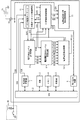
以下、本発明を適用した具体的な実施の形態について、図面を参照しながら詳細に説明する。図1に本実施の形態にかかる半導体集積回路1のブロック構成を示す。
Hereinafter, specific embodiments to which the present invention is applied will be described in detail with reference to the drawings. FIG. 1 shows a block configuration of a semiconductor integrated
図1に示すように、半導体集積回路1は、CPU2と、ROM3と、メモリ4と、発振器5と、割込み回路6と、低周波発振器7と、電圧検出レベル記憶回路8と、電源電圧検出レベル切替回路9と、電源電圧検出回路10と、低周波クロック制御回路11と、STOP解除制御回路12と、電源電圧降下用擬似負荷回路13とを有する。
As shown in FIG. 1, the semiconductor integrated
半導体集積回路1の各構成要素は、通常動作時では電池が供給する電源電圧VDDで動作し、電池が抜かれた状態では、外付けのコンデンサ15が供給する電源電圧VDDで動作する。なお、電源電圧VDDがコンデンサ15で供給される場合は、コンデンサ15が蓄えている電力に限度があるため、通常動作時よりも低消費電力の後述するSTOP状態(低消費電力モード)で、動作する。
Each component of the semiconductor integrated
また、半導体集積回路1は、STOP状態を解除する外部のSTOP解除キー38と接続される。ストップ解除キー38は、半導体集積回路1のSTOP状態を解除する場合、STOP解除キー入力信号S38をロウレベルとする。
Further, the semiconductor integrated
メモリ4は、CPU2が演算処理するプログラムやデータ等が展開される。メモリ4は、揮発性記憶装置であり、最低動作電圧以下となると記憶しているデータ等の保持ができなくなる。例えば、半導体集積回路1が、外付けコンデンサ15が供給する電源電圧VDDで動作するとき、コンデンサ15の供給する電源電圧VDDが低下し、最低動作電圧以下となると記憶しているデータが破壊される可能性がある。
The
ROM3は、不揮発性記憶装置であり、プログラムやデータ等を保持する。
The
発振器5は、CPU2、ROM3、メモリ4等の通常動作時の動作クロックを生成する。
The
低周波発振器7は、STOP状態(後述)の低周波クロック信号CLKを生成する。
The
CPU2は、中央演算装置であり、半導体集積回路1のシステムを制御する。CPU2は、ROM3等から読み出されメモリ4に展開されるプログラムやデータに応じて演算処理を行う。また、半導体集積回路1のシステムをSTOP状態とするSTOP信号S36を出力する。このSTOP信号S36がハイレベルでSTOP状態、STOP信号S36がロウレベルでSTOP解除状態となる。
The
ここで、STOP状態とは、半導体集積回路1を低消費電力モードとするため、発振器5を停止することで、ROM3、メモリ4等のCPU2の周辺回路のクロック動作を停止し、且つ、低周波発振器7の生成する低周波クロックでCPU2、ウォッチドックタイマ(不図示)等の最小限のシステムのみを動作させる状態とする。また、STOP解除状態とは、このSTOP状態を解除した通常動作の状態である。
Here, the STOP state means that the semiconductor integrated
割込み回路6は、STOP解除信号S23に応じて、CPU2に対してSTOP解除状態とさせる割込み制御を行う。
The interrupt
電源電圧検出回路10は、抵抗16〜25と、電源検出スイッチ回路26〜34と、基準電圧回路35と、コンパレータ36、37とを有する。
The power supply
抵抗16は、ノードN25と接地端子GNDとの間に接続される。抵抗17は、ノードN25とN26との間に接続される。抵抗18は、ノードN26とN27との間に接続される。抵抗19は、ノードN27とN28との間に接続される。抵抗20は、ノードN28とN29との間に接続される。抵抗21は、ノードN29とN30との間に接続される。抵抗22は、ノードN30とN31との間に接続される。抵抗23は、ノードN31とN32との間に接続される。抵抗24は、ノードN32とN33との間に接続される。抵抗25は、ノードN33と電源端子VDDとの間に接続される。ノードN25〜N33で抵抗分圧される電圧を、それぞれS25〜S33とする。
電源検出スイッチ回路26は、ノードN25とN34との間に接続され、スイッチON信号S5に応じてON状態が制御される。電源検出スイッチ回路27は、ノードN26とN34との間に接続され、スイッチON信号S6に応じてON状態が制御される。電源検出スイッチ回路28は、ノードN27とN34との間に接続され、スイッチON信号S7に応じてON状態が制御される。電源検出スイッチ回路29は、ノードN28とN34との間に接続され、スイッチON信号S8に応じてON状態が制御される。電源検出スイッチ回路30は、ノードN29とN34との間に接続され、スイッチON信号S9に応じてON状態が制御される。電源検出スイッチ回路31は、ノードN30とN34との間に接続され、スイッチON信号S10に応じてON状態が制御される。電源検出スイッチ回路32は、ノードN31とN34との間に接続され、スイッチON信号S11に応じてON状態が制御される。電源検出スイッチ回路33は、ノードN32とN34との間に接続され、スイッチON信号S12に応じてON状態が制御される。電源検出スイッチ回路34は、ノードN33とN34との間に接続され、スイッチON信号S13に応じてON状態が制御される。
The power
電源検出スイッチ回路26〜34は、スイッチON信号S5〜S13に応じて何れか1つがオン状態となる。このため、電源検出電圧S34は、オンした電源検出スイッチ回路に対応する抵抗分圧となる。例えば、電源検出スイッチ回路33がオン状態となると、電源検出電圧S34は、抵抗分圧S32となる。
Any one of the power
コンパレータ36は、ノードN34の電圧(以下、電源検出電圧と称す)と、基準電圧回路35の生成する基準電圧S35とを比較し、電源電圧検出出力S14を出力する。例えば、基準電圧S35>電源検出電圧S34となると、電源電圧検出出力S14はハイレベルとなる。逆に、基準電圧S35<電源検出電圧S34となるとロウレベル出力する。
The
コンパレータ37は、抵抗分圧されたノードN33の電圧と、基準電圧回路35の生成する基準電圧S35とを比較し、POC出力S22を出力する。例えば、基準電圧S35>ノードN33の電圧S33となると、POC出力S22はハイレベルとなる。逆に、基準電圧S35<ノードN33の電圧S33となると、POC出力S22はロウレベルとなる。POC出力S22がハイレベルとなる場合、半導体集積回路1のシステム全体がリセット(パワーオンクリア)される。
The
電源電圧検出レベル切替回路9は、デコード回路39と、電圧検出レベル切換えセレクタ40と、OR回路41とを有する。
The power supply voltage detection
デコード回路39は、レジスタ信号S2、S3、S4に応じて、デコード回路出力信号S39〜S46の何れか1つをハイレベルとして出力する。なお、これ以降、レジスタ信号S2、S3、S4を、必要に応じて(S4、S3、S2)と記載する。なお、「0」はロウレベル、「1」はハイレベルを表す。デコード回路39は、例えば、(S4、S3、S2)=(1、1、1)ではデコード回路出力信号S39、(S4、S3、S2)=(1、1、0)ではデコード回路出力信号S40、(S4、S3、S2)=(1、0、1)ではデコード回路出力信号S41、(S4、S3、S2)=(1、0、0)ではデコード回路出力信号S42、(S4、S3、S2)=(0、1、1)ではデコード回路出力信号S43、(S4、S3、S2)=(0、1、0)ではデコード回路出力信号S44、(S4、S3、S2)=(0、0、1)ではデコード回路出力信号S45、(S4、S3、S2)=(0、0、0)ではデコード回路出力信号S46をハイレベルとする。
The
OR回路41は、デコード回路出力信号S45、S46を入力し、OR演算結果を出力する。
The OR
電圧検出レベル切換えセレクタ40は、検出レベル切換え信号S18に応じて、スイッチON信号S5〜S13の値を、それぞれデコード回路出力信号S39〜S46の値、ロウレベル(GND)、もしくは、それぞれロウレベル、ロウレベル、デコード回路出力信号S39〜S44の値、OR回路41の出力値のどちらかとして出力する。
In response to the detection level switching signal S18, the voltage detection
電圧検出レベル記憶回路8は、フリップフロップ回路42〜45と、AND回路46と、インバータ回路76〜81とを有する。
The voltage detection
フリップフロップ回路42は、データ入力端子Dにインバータ回路79の出力信号、クロック入力端子に低周波クロックCKL3、リセット端子RにSTOP解除制御リセット信号S15を入力し、データ出力端子Qからレジスタ信号S2を出力する。
The flip-
フリップフロップ回路43は、データ入力端子Dにインバータ回路80の出力信号、クロック入力端子にレジスタ信号S2、リセット端子RにSTOP解除制御リセット信号S15を入力し、データ出力端子Qからレジスタ信号S3を出力する。
The flip-
フリップフロップ回路44は、データ入力端子Dにインバータ回路81の出力信号、クロック入力端子にレジスタ信号S3、リセット端子RにSTOP解除制御リセット信号S15を入力し、データ出力端子Qからレジスタ信号S4を出力する。
The flip-
フリップフロップ回路45は、データ入力端子Dにハイレベル(電源電圧VDD)、クロック入力端子にインバータ回路77の出力、リセット端子RにSTOP解除制御リセット信号S15を入力し、データ出力端子Qから信号S47を出力する。
The flip-
インバータ回路76は、電源電圧検出出力S14を入力し、その反転信号を出力する。インバータ回路77は、低周波クロックCLK3を入力し、その反転信号を出力する。インバータ回路79は、レジスタ信号S2を入力し、その反転信号を出力する。インバータ回路80は、レジスタ信号S3を入力し、その反転信号を出力する。インバータ回路81は、レジスタ信号S4を入力し、その反転信号を出力する。
The
AND回路46は、インバータ回路76の出力と信号S47とを入力し、演算結果をレジスタ初期値処理信号S16として出力する。
The AND
STOP解除制御回路12は、フリップフロップ回路55〜59と、AND回路53、54と、インバータ回路78とを有する。
The STOP
AND回路54は、レジスタ初期値処理信号S16と低周波クロックCKL2とを入力し、演算結果を低周波クロックCLK4として出力する。
The AND
フリップフロップ回路55は、データ入力端子Dにハイレベル(電源電圧VDD)、クロック入力端子に低周波クロックCLK4、リセット端子RにSTOP解除制御リセット信号S15を入力し、データ出力端子Qから検出レベル切替信号S18を出力する。
The flip-
フリップフロップ回路56は、データ入力端子Dに検出レベル切替信号S18、クロック入力端子に低周波クロックCKL2、リセット端子RにSTOP解除制御リセット信号S15を入力し、データ出力端子Qから擬似負荷ON開始信号S20を出力する。
The flip-
フリップフロップ回路57は、データ入力端子Dに擬似負荷ON開始信号S20、クロック入力端子に低周波クロックCKL2、リセット端子RにSTOP解除制御リセット信号S15を入力し、データ出力端子Qから擬似負荷OFF信号S21を出力する。
The flip-
フリップフロップ回路58は、データ入力端子Dに擬似負荷OFF信号S21、クロック入力端子に低周波クロックCKL2、リセット端子RにSTOP解除制御リセット信号S15を入力し、データ出力端子Qから信号S49を出力する。
The flip-
フリップフロップ回路59は、データ入力端子Dに信号S49、クロック入力端子に低周波クロックCKL2、リセット端子RにSTOP解除制御リセット信号S15を入力し、データ出力端子Qから判定処理終了信号S17を出力する。
The flip-
インバータ回路78は、電源電圧検出出力S14を入力し、その反転信号を出力する。
The
AND回路53は、インバータ回路78の出力信号と信号S49とを入力し、演算結果をSTOP解除信号S23として出力する。
The AND
電源電圧降下用擬似負荷回路13は、AND回路60と、抵抗61と、NPNトランジスタ62と、インバータ回路82とを有する。
The power supply voltage drop
インバータ回路82は、擬似負荷OFF信号S21を入力し、その反転信号を出力する。
The
AND回路60は、インバータ回路82の出力信号と擬似負荷ON開始信号S20とを入力し、演算結果をNPNトランジスタ62のベースに出力する。
The AND
抵抗61は、電源配線S24とNPNトランジスタ62のコレクタに接続される。なお、電源配線S24からは、コンデンサ15の電源電圧VDDが供給される。
The resistor 61 is connected to the power supply line S24 and the collector of the
NPNトランジスタ62は、コレクタが抵抗61、エミッタが接地端子GNDに接続され、ベースにAND回路60の出力が入力される。NPNトランジスタ62がオンすると、抵抗61に電流が流れる。このとき、電源電圧VDDがコンデンサ15のみから供給されている場合、抵抗61、NPNトランジスタ62に流れる電流により、電源電圧VDDが低下する。このNPNトランジスタ62がオン時に流れる電流は、抵抗61の抵抗値に応じて調整可能である。半導体集積回路1が通常動作時に電源電圧VDDから流れる電流よりも十分小さい電流値に制限されるように調整される。
In the
低周波クロック制御回路11は、CPU2からのSTOP信号S36がハイレベルとなった場合、STOP解除制御リセット信号S15をロウレベルとする。また、判定処理終了信号S17がハイレベルとなった場合、STOP解除制御リセット信号S15をハイレベルとする。なお、STOP解除制御リセット信号S15がハイレベルの場合は、電圧検出レベル記憶回路8、STOP解除制御回路12のフリップフロップ回路42〜45、55〜59のリセット端子に入力され、フリップフロップ回路42〜45、55〜59が初期化され、それらフリップフロップ回路の出力がロウレベルとなる。
When the STOP signal S36 from the
また、低周波クロック制御回路11は、STOP解除キーラッチを有する。STOP解除キーラッチは、ストップ解除キー38が生成するSTOP解除キー入力信号S38のハイレベルからロウレベルへの立ち下がりをトリガに、STOP解除キー入力信号S38をラッチする。
The low frequency
そして、低周波クロック制御回路11は、このSTOP解除キー入力信号S38をラッチした信号に応じた信号と、低周波発振器7からの低周波クロックCLKで同期をとった信号と、STOP信号S36とをAND演算し、低周波クロックCLK2を生成する。なお、上記STOP解除キー入力信号S38をラッチした信号に応じた信号とは、例えば、STOP解除キー入力信号S38をラッチした信号をインバータにより、反転した信号である。
Then, the low frequency
また、低周波クロック制御回路11は、低周波クロックCLK2と、検出レベル切換え信号S18を反転した信号とを、AND演算し、低周波クロックCLK3を生成する。例えば、検出レベル切換え信号S18がロウレベルのとき、低周波クロックCLK3が生成され、検出レベル切換え信号S18がハイレベルのとき、低周波クロックCLK3が生成されずロウレベルに固定される。
Further, the low frequency
次に、上記半導体集積回路1の動作を説明する。図7に半導体集積回路1の動作タイミングチャートの一例を示す。この動作タイミングチャートの例では、電源検出スイッチ回路29がオンする電源電圧VDD範囲の場合において、電源電圧降下用擬似負荷回路13によって電源電圧低下の判定がなされたときにSTOP解除しない場合を示す。なお、本例の前提として電源電圧VDDを3.1Vとする。
Next, the operation of the semiconductor integrated
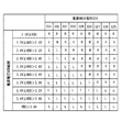
また、図8に、電源電圧VDD範囲と抵抗分圧S25〜S33の選択による電源電圧検出回路10が出力する電源電圧検出出力S14の信号レベルの表を示す。なお、図8では、電源電圧検出出力S14がロウレベル出力される場合は"L"、ハイレベル出力される場合は"H"と記載する。
FIG. 8 shows a table of signal levels of the power supply voltage detection output S14 output from the power supply
図7の時刻T1は、STOP状態に入る前のSTOP解除状態である。時刻T2は、STOP状態である。時刻T3は、STOP解除キーがラッチされた状態と電源検出レベルの電源検出スイッチ回路26がONの状態である。時刻T4は、電源検出レベルの電源検出スイッチ回路27がONの状態である。時刻T5は、電源検出レベルの電源検出スイッチ回路28がONの状態である。時刻T6は、電源検出スイッチ回路28のON時に電源電圧検出出力S14がロウレベルに変化したことで、擬似負荷をONする前の電源電圧VDD範囲を記憶した状態と電源検出スイッチ回路28から電源検出スイッチ回路30をONにし、検出レベルを低下した状態である。時刻T7は、擬似負荷をONし始めた状態である。時刻T8は、擬似負荷をOFFした状態である。時刻T9は、電源電圧VDD検出レベルに応じて判定し、STOP解除信号を出力する状態である。時刻T10は、電源電圧VDDの判定が終了し、保持されたフリップフロップ回路にリセットをかけ、STOP解除キーを待つ状態である。
Time T1 in FIG. 7 is a STOP release state before entering the STOP state. Time T2 is in the STOP state. At time T3, the STOP release key is latched and the power
まず、STOP状態に入る前のSTOP解除状態の時刻T1について説明する。この時点では、CPU2からのSTOP信号S36がロウレベルであり、STOP解除制御リセット信号S15がハイレベルになる。ハイレベルのSTOP解除制御リセット信号S15が、電圧検出レベル記憶回路8、STOP解除制御回路12のフリップフロップ回路42〜45、55〜59のリセット端子に入力され、フリップフロップ回路42〜45、55〜59が初期化される。このため、レジスタ信号S2、S3、S4、信号S47、検出レベル切換え信号S18、擬似負荷ON開始信号S20、擬似負荷OFF信号S21、擬似負荷ON後の検出レベル判定開始信号S49、判定処理終了信号S17はロウレベルとなる。
First, the time T1 in the STOP release state before entering the STOP state will be described. At this time, the STOP signal S36 from the
また、上記のようにレジスタ信号(S4、S3、S2)=(0、0、0)となるため、電源電圧検出レベル切替回路9のデコード回路39が出力するデコード回路出力信号S46のみがハイレベルになる。検出レベル切換え信号S18がロウレベルであり、電圧検出レベル切換えセレクタ40から出力されるスイッチON信号S12のみがハイレベルになり、電源電圧検出回路10の電源検出スイッチ回路33のみがONする。
Since the register signals (S4, S3, S2) = (0, 0, 0) as described above, only the decode circuit output signal S46 output from the
ここで、抵抗16〜25の抵抗分圧S25〜S33を具体的な電源電圧VDDを元に説明する。
Here, the resistance voltage divisions S25 to S33 of the
上述したように電源検出スイッチ回路33のみがONされる状態では、抵抗分圧S32が選択され電源検出電圧S34となり、電源電圧VDDが3.1Vなので、図8に示すように、電源電圧検出出力S14はロウレベルになる。
In the state where only the power supply
そして、ロウレベルの電源電圧検出出力S14が、電圧検出レベル記憶回路8のインバータ回路76に入力され、その出力はハイレベルになる。AND回路46は、ハイレベルのインバータ回路76の出力、ロウレベルのフリップフロップ回路45の出力信号S47を入力し、ロウレベルのレジスタ初期値処理信号S16を出力する。
Then, the low-level power supply voltage detection output S14 is input to the
低周波クロック制御回路11からの低周波クロックCLK2、CLK3はSTOP状態で出力され、時刻T1のタイミングではロウレベルとなる。また、STOP解除制御回路12の2入力AND回路53に入力する擬似負荷ON後の検出レベル判定開始信号S49がロウレベルのため、STOP解除信号S23はロウレベルとなる。
The low frequency clocks CLK2 and CLK3 from the low frequency
電源電圧降下用擬似負荷回路13のAND回路60に入力される擬似負荷ON開始信号S20がロウレベルであるため、AND回路60の出力である擬似負荷ON信号S50もロウレベルとなる。NPNトランジスタ62は、擬似負荷ON信号S50がロウレベルのため、電流が流れていないOFF状態である。
Since the pseudo load ON start signal S20 input to the AND
次に、STOP状態となった時刻T2の状態について説明する。まず、時刻T2前に、CPU2からハイレベルのSTOP信号S36が出力され半導体集積回路1はSTOP状態になる。そして、STOP解除制御リセット信号S15がハイレベルからロウレベルになる。このSTOP状態において、電池が抜き取られて、半導体集積回路1は、コンデンサ15のみによる電源電圧VDDで動作する(図1のブロック図の状態)。
Next, the state at time T2 when the STOP state is set will be described. First, before time T2, a high-level STOP signal S36 is output from the
この状態でSTOP解除キー38のスイッチが押され、STOP解除キー入力信号S38がハイレベルからロウレベルに変化する。STOP解除キー38は、通常ハイレベルにプルアップされているものとする。なお、従来技術では、コンデンサにより電源電圧を供給しているにもかかわらず、STOP解除キーによりSTOP状態を解除したような場合に、コンデンサが供給する電源電圧が低下し、装置が誤動作を引き起こす問題が発生していた。
In this state, the switch of the
そして、STOP解除キー入力信号S38のロウレベルへの立ち下がりをトリガにしてSTOP解除キー入力信号S38をラッチする。時刻T2のタイミングで、STOP解除キー入力信号S38をラッチした信号に応じた信号と、低周波クロックCLKで同期をとった信号と、STOP信号S36とをAND演算することで作成される低周波クロックCLK2が、低周波クロック制御回路11から出力される。
Then, the STOP cancellation key input signal S38 is latched with the falling edge of the STOP cancellation key input signal S38 to the low level as a trigger. A low-frequency clock generated by ANDing the signal corresponding to the signal obtained by latching the STOP release key input signal S38, the signal synchronized with the low-frequency clock CLK, and the STOP signal S36 at the time T2. CLK2 is output from the low-frequency
また、低周波クロックCLK2と、検出レベル切換え信号S18を反転した信号とを、AND演算することで作成される低周波クロックCLK3が、低周波クロック制御回路11から出力される。
Further, the low frequency
この低周波クロックCLK3の立ち上がりで、時刻T2に電圧検出レベル記憶回路8のフリップフロップ回路42は、インバータ回路79が出力するレジスタ信号S2の反転信号をラッチする。このため、出力のレジスタ信号S2が、ロウレベルからハイレベルに遷移する。なお、レジスタ信号S2は、この後、低周波クロックCLK2の立ち上がり毎に出力レベルが反転する。
At the rising edge of the low frequency clock CLK3, the flip-
フリップフロップ回路43は、レジスタ信号S2の立ち上がりで、インバータ回路80が出力するレジスタ信号S3の反転信号をラッチする。このため、出力のレジスタ信号S3が、ロウレベルからハイレベルに遷移する。なお、レジスタ信号S3は、この後、レジスタ信号S2の立ち上がり毎に出力レベルが反転する。つまり、低周波クロックCLK2の立ち上がり2回毎に出力レベルが反転する。
The flip-
フリップフロップ回路44は、レジスタ信号S3の立ち上がりで、インバータ回路81が出力するレジスタ信号S4の反転信号をラッチする。このため、出力のレジスタ信号S4が、ロウレベルからハイレベルに遷移する。なお、レジスタ信号S4は、この後、レジスタ信号S3の立ち上がり毎に出力レベルが反転する。つまり、低周波クロックCLK2の立ち上がり4回毎に出力レベルが反転する。
The flip-
時刻T2において、(S4、S3、S2)=(1、1、1)になり、電源電圧検出レベル切替回路9のデコード回路39の出力信号はデコード回路出力信号S39のみがハイレベルになる。このため、電圧検出レベル切換えセレクタ40から出力されるスイッチON信号S5のみがハイレベルになる。
At time T2, (S4, S3, S2) = (1, 1, 1), and only the decode circuit output signal S39 becomes the high level as the output signal of the
そして、スイッチON信号S5のみがハイレベルになることから、電源電圧検出回路10の電源検出スイッチ回路26のみがONし、抵抗分圧S25が選択される。ここで、電源電圧VDDが3.1Vであるので、図8より電源電圧検出出力S14はロウレベルからハイレベルに遷移する。
Since only the switch ON signal S5 becomes high level, only the power supply
電圧検出レベル記憶回路8のフリップフロップ回路45は、クロック入力端子にインバータ回路77を経由して低周波クロックCLK3を入力する。このため、時刻T2のタイミングでは、フリップフロップ回路45は、クロック入力端子に立ち下がりのクロックが入力され、データ入力端子Dのハイレベルを取り込まず、出力信号S47はロウレベルのままとなる。よって、時刻T2のタイミングで、電源電圧検出出力S14がロウレベルで出力される期間のレジスタ初期値処理信号S16のハイレベルへの変化を止める。
The flip-
そして、時刻T2のタイミングより低周波クロックCLKの半クロック後で、インバータ回路77を介して、フリップフロップ回路45のクロック入力端子に立ち上がり入力され、フリップフロップ回路45はハイレベルのデータを取り込む。このため、信号S47はロウレベルからハイレベルに遷移する。この信号S47と、インバータ回路76の出力とをAND演算するAND回路46から出力されるレジスタ初期値処理信号S16は、圧検出出力S14がハイレベルからロウレベルに遷移するまで、ロウレベルのままとなる。
Then, after a half clock of the low frequency clock CLK from the timing of the time T2, it rises and is input to the clock input terminal of the flip-
次に、電源検出レベルの電源検出スイッチ回路26がON状態の時刻T3について説明する。
Next, the time T3 when the power
時刻T3のタイミングで、電圧検出レベル記憶回路8のフリップフロップ回路42に入力する低周波クロックCLK3が立ち上がり、インバータ回路79が出力するロウレベルのデータをラッチする。このため、レジスタ信号S2が、ハイレベルからロウレベルに遷移し、(S4、S3、S2)=(1、1、0)になる。
At the timing of time T3, the low frequency clock CLK3 input to the flip-
これにより、電源電圧検出レベル切替回路9のデコード回路39の出力信号はデコード回路出力信号S40のみがハイレベルになる。このため、電圧検出レベル切換えセレクタ40から出力されるスイッチON信号S6のみがハイレベルになる。
As a result, only the decode circuit output signal S40 becomes the high level as the output signal of the
そして、スイッチON信号S6のみがハイレベルになることから、電源電圧検出回路10の電源検出スイッチ回路27のみがONし、抵抗分圧S26が選択される。ここで、電源電圧VDDが3.1Vであるので、図8より電源電圧検出出力S14はハイレベルのままのため、レジスタ初期値処理信号S16もロウレベルのままになる。
Since only the switch ON signal S6 becomes high level, only the power supply
次に、電源検出レベルの電源検出スイッチ回路27がON状態の時刻T4について説明する。
Next, the time T4 when the power
時刻T4のタイミングでもフリップフロップ回路42に入力する低周波クロックCLK3が立ち上がり、インバータ回路79が出力するハイレベルのデータをラッチする。このため、レジスタ信号S2がロウレベルからハイレベルに遷移し、フリップフロップ回路43が、インバータ回路79が出力するロウレベルのデータをラッチする。このため、(S4、S3、S2)=(1、0、1)になり、電源電圧検出レベル切替回路9のデコード回路39の出力信号はデコード回路出力信号S41のみがハイレベルになる。このため、電圧検出レベル切換えセレクタ40から出力されるスイッチON信号S7のみがハイレベルになる。
Also at the timing of time T4, the low frequency clock CLK3 input to the flip-
そして、スイッチON信号S7のみがハイレベルになることから、電源電圧検出回路10の電源検出スイッチ回路28のみがONし、抵抗分圧S27が選択される。ここで、電源電圧VDDが3.1Vであるので、図8より電源電圧検出出力S14はハイレベルのままのため、レジスタ初期値処理信号S16もロウレベルのままになる。
Since only the switch ON signal S7 is at a high level, only the power supply
次に、電源検出レベルの電源検出スイッチ回路28がON状態の時刻T5について説明する。
Next, time T5 when the power
時刻T5のタイミングでもフリップフロップ回路42に入力する低周波クロックCLK3が立ち上がり、インバータ回路79が出力するロウレベルのデータをラッチする。このため、レジスタ信号S2が、ハイレベルからロウレベルに遷移し、(S4、S3、S2)=(1、0、0)になる。
Even at the timing of time T5, the low-frequency clock CLK3 input to the flip-
これにより、電源電圧検出レベル切替回路9のデコード回路39の出力信号はデコード回路出力信号S42のみがハイレベルになる。このため、電圧検出レベル切換えセレクタ40から出力されるスイッチON信号S8のみがハイレベルになる。
As a result, only the decode circuit output signal S42 becomes the high level as the output signal of the
そして、スイッチON信号S8のみがハイレベルになることから、電源電圧検出回路10の電源検出スイッチ回路29のみがONし、抵抗分圧S28が選択される。ここで、電源電圧VDDが3.1Vであるので、図8より電源電圧検出出力S14はハイレベルからロウレベルに遷移する。
Since only the switch ON signal S8 is at a high level, only the power supply
次に、電源検出スイッチ回路28のON状態時に電源電圧検出出力S14がロウレベルに変化したことで擬似負荷をONする前の電源電圧VDD範囲を記憶した状態と、電源検出スイッチ回路30をONし検出レベルを低下した状態の時刻T6について説明する。なお、この時刻T6は、上述した電源電圧検出出力S14がハイレベルからロウレベルに遷移したタイミングである。
Next, when the power supply
電源電圧検出出力S14のロウレベルになり、AND回路46が出力するレジスタ初期値処理信号S16がロウレベルからハイレベルに遷移する。そして、そのレジスタ初期値処理信号S16が、STOP解除制御回路12のAND回路54に入力される。AND回路54は、一方の入力に低周波クロックCLK2を入力しているため、レジスタ初期値処理信号S16がハイレベルに遷移した時刻T6のタイミングで、低周波クロックCLK4を出力する。
The power supply voltage detection output S14 becomes low level, and the register initial value processing signal S16 output from the AND
この低周波クロックCLK4がフリップフロップ回路55のクロック入力端子に入力され、低周波クロックCLK4の立ち上がりのタイミングで、フリップフロップ回路55がハイレベルのデータをラッチする。このため、フリップフロップ回路55の出力である検出レベル切換え信号S18がロウレベルからハイレベルに遷移する。検出レベル切換え信号S18がハイレベルになることにより、低周波クロック制御回路11から出力される低周波クロックCLK3はロウレベルに固定される。
The low-frequency clock CLK4 is input to the clock input terminal of the flip-
低周波クロックCLK3がロウレベルに固定されると、電圧検出レベル記憶回路8のフリップフロップ回路42から出力されるレジスタ信号S2の値も固定される。更に、フリップフロップ回路43から出力されるレジスタ信号S3の値、フリップフロップ回路44から出力されるレジスタ信号S4の値も固定され、(S4、S3、S2)=(1、0、0)となる。この状態が、電源電圧降下用擬似負荷回路13の擬似負荷で電流を流す前の電源電圧VDDの範囲を検出し、記憶した状態である。
When the low frequency clock CLK3 is fixed at the low level, the value of the register signal S2 output from the flip-
そして、(S4、S3、S2)=(1、0、0)が固定されデコード回路出力信号S42のみがハイレベルの状態で、検出レベル切換え信号S18がハイレベルとなることから、電圧検出レベル切換えセレクタ40のセレクタが切り替わる。このため、電圧検出レベル切換えセレクタ40から出力されるスイッチON信号S10のみがハイレベルの状態に切り替わる。そして、スイッチON信号S10により、電源検出スイッチ回路31がONし、抵抗分圧S30が選択される。
Since (S4, S3, S2) = (1, 0, 0) is fixed and only the decode circuit output signal S42 is at a high level, the detection level switching signal S18 is at a high level. The selector of the
上記抵抗分圧S30が選択されることになり図8より、電源電圧検出出力S14がロウレベルの限界電圧は「2.8V≧VDD>2.6V」になる。この状態が、擬似負荷で電流を流した後に電源電圧VDDが低下するか判断するための、電源電圧VDDを降下させる前に記憶した電源電圧レベルに応じて低下させた変更レベルになる。 The resistance voltage division S30 is selected, and from FIG. 8, the limit voltage of the low level of the power supply voltage detection output S14 becomes “2.8V ≧ VDD> 2.6V”. This state is a change level that is lowered in accordance with the power supply voltage level stored before the power supply voltage VDD is lowered to determine whether the power supply voltage VDD is lowered after the current is passed through the pseudo load.
次に、擬似負荷をONし始めた状態の時刻T7について説明する。 Next, the time T7 when the pseudo load is turned on will be described.
STOP解除制御回路12において、時刻T7のタイミングで、低周波クロックCLK2の立ち上がりにより、検出レベル切換え信号S18のハイレベルをフリップフロップ回路56がラッチする。このため、擬似負荷ON開始信号S20がロウレベルからハイレベルに遷移する。
In the STOP
擬似負荷ON開始信号S20がロウレベルからハイレベルに遷移することで、電源電圧降下用擬似負荷回路13のAND回路60の出力である擬似負荷ON信号S50がハイレベルになりNPNトランジスタ62がONする。このため、電源配線S24に接続された抵抗61により制限された電流が流れる。
As the pseudo load ON start signal S20 transitions from the low level to the high level, the pseudo load ON signal S50, which is the output of the AND
次に、擬似負荷をOFFした状態の時刻T8について説明する。 Next, time T8 in a state where the pseudo load is turned off will be described.
時刻T8のタイミングで、擬似負荷ON開始信号S20のハイレベルをフリップフロップ回路57がラッチする。このため、擬似負荷OFF信号S21がロウレベルからハイレベルに遷移する。
At the timing of time T8, the flip-
擬似負荷OFF信号S21がロウレベルからハイレベル遷移することで、電源電圧降下用擬似負荷回路13のAND回路60の出力である擬似負荷ON信号S50がロウレベルになることでNPNトランジスタ62がOFFし、電流を流すことを止める。
When the pseudo load OFF signal S21 transits from a low level to a high level, the pseudo load ON signal S50, which is the output of the AND
ここで、半導体集積回路1がコンデンサ15にて供給された電圧のみで動作しているため、電源電圧VDDが3.1Vから電圧が低下する。そして、時刻T7〜T8の期間で、電源電圧VDDが「2.8V≧VDD>2.6V」まで低下したとき、電源電圧検出出力S14がハイレベルになる。そして、この時点でSTOP解除制御回路12のAND回路53に入力する擬似負荷ON後の検出レベル判定開始信号S49がロウレベルのため、STOP解除信号S23はロウレベルになる。
Here, since the semiconductor integrated
次に、電源電圧検出レベルに応じて判定し、STOP解除信号S23を出力する状態の時刻T9について説明する。 Next, the time T9 in which the determination is made according to the power supply voltage detection level and the STOP release signal S23 is output will be described.
時刻T9のタイミングで、擬似負荷OFF信号S21のハイレベルを、フリップフロップ回路58がラッチする。このため、擬似負荷ON後の検出レベル判定開始信号S49がロウレベルからハイレベルに遷移する。
At the timing of time T9, the flip-
電源電圧検出出力S14がハイレベルのため、擬似負荷ON後の検出レベル判定開始信号S49がロウレベルからハイレベルに遷移することで、AND回路53の出力であるSTOP解除信号S23は、ロウレベルのままとなる。このため、割込み回路6に対して割り込み動作を発生させず、CPU2からのSTOP信号S36がハイレベルを保持し、STOP解除しない。
Since the power supply voltage detection output S14 is at a high level, the detection level determination start signal S49 after the pseudo load is turned on transitions from the low level to the high level, so that the STOP release signal S23 that is the output of the AND
これは低下させた変更検出レベルまで電源電圧VDDが低下したことで、電源電圧VDDをコンデンサ15のみで供給していると判断し、STOP解除を行わない制御を行うためである。
This is because it is determined that the power supply voltage VDD is supplied only by the
次に、電源電圧VDDの判定が終了し、保持されたフリップフロップ回路にリセットをかけ、STOP解除キーを待つ状態の時刻T10について説明する。 Next, the time T10 when the determination of the power supply voltage VDD is completed, the held flip-flop circuit is reset, and a STOP release key is waited for will be described.
時刻T10のタイミングで、擬似負荷ON後の検出レベル判定開始信号S49のハイレベルをフリップフロップ回路59がラッチする。このため、判定処理終了信号S17がロウレベルからハイレベルに遷移する。
At the timing of time T10, the flip-
判定処理終了信号S17がロウレベルからハイレベルに遷移するため、低周波クロック制御回路11の出力のSTOP解除制御リセット信号S15はハイレベルになる。STOP解除制御リセット信号S15がハイレベルになりフリップフロップ回路42〜44、55〜59が、リセットされて、初期化されSTOP解除待ちの状態にもどる。
Since the determination processing end signal S17 transits from the low level to the high level, the STOP cancellation control reset signal S15 output from the low frequency
尚、時刻T7〜T8の期間、擬似負荷ON後も「2.8V≧VDD>2.6V」まで電源電圧VDDが低下しない場合は、電源電圧検出出力S14はロウレベルである。そして、擬似負荷ON後の検出レベル判定開始信号S49がハイレベルになることで、STOP解除信号S23はハイレベルになる。割込み回路6にハイレベルのSTOP解除信号S23が入力され、CPU2からのSTOP信号S36がロウレベルになり、STOP状態を解除する。
In the period from time T7 to time T8, when the power supply voltage VDD does not decrease to “2.8V ≧ VDD> 2.6V” even after the pseudo load is turned on, the power supply voltage detection output S14 is at a low level. Then, when the detection level determination start signal S49 after the pseudo load is turned on becomes high level, the STOP release signal S23 becomes high level. A high-level STOP cancellation signal S23 is input to the interrupt
これは低下させた変更検出レベルまで電源電圧VDDが低下しないことで、電源電圧VDDをコンデンサ15のみで供給していない状態(電池が接続されいる状態)であると判断し、STOP解除を行う制御を行うためである。 This is because the power supply voltage VDD does not drop to the lowered change detection level, so that it is determined that the power supply voltage VDD is not supplied only by the capacitor 15 (the battery is connected), and the STOP is released. Is to do.
また、擬似負荷で電流を流す前の電源電圧VDDが最初から低い場合、例えば電源電圧VDDが2.3Vの場合はPOC(パワーオンクリア)が発生する電圧2.0Vに近いため、擬似負荷で電流を流すことで電源電圧VDDが低下し、2.0V以下(但し、半導体集積回路1の最低動作電圧より高いとする)になりPOC出力S22をハイレベルにする。POC出力S22をハイレベルにすることで、半導体集積回路1内部のCPU2と周辺回路が初期化され、発振器5、低周波発振器7が停止状態になり、メモリ4はアクセスが停止し、揮発メモリのRAMはデータ保持されている状態(以降リセット状態と称する)となる。
In addition, when the power supply voltage VDD is low from the beginning before the current flows in the pseudo load, for example, when the power supply voltage VDD is 2.3 V, it is close to the voltage of 2.0 V at which POC (power on clear) occurs. By supplying a current, the power supply voltage VDD is lowered to 2.0 V or less (provided that it is higher than the minimum operating voltage of the semiconductor integrated circuit 1), and the POC output S22 is set to the high level. By setting the POC output S22 to the high level, the
ここで、擬似負荷で電流を流した後に電源電圧VDDが降下するか判断する検出レベルの設定の例を説明する。コンデンサ15をCとし、NPNトランジスタ62と抵抗61の合成抵抗の擬似負荷をRとし、擬似負荷で電流を流している時間をtとする。そして、擬似負荷で電流を流す前の電圧レベルをV0として、低下させる検出レベルをVとした関係式は以下のようになる。
Here, an example of setting a detection level for determining whether or not the power supply voltage VDD drops after flowing a current with a pseudo load will be described. The
V=V0×exp(−t/(R×C)) V = V0 × exp (−t / (R × C))
このとき、t=2mS、R=300Ω、V0=3.1V、C=47μFとした場合、 At this time, when t = 2 mS, R = 300Ω, V0 = 3.1 V, and C = 47 μF,
V=3.1V×exp(−2mS/(300Ω×47μF))=2.69となり、V0より約0.4V低下する。このことから、擬似負荷Rで電流を流した後に電源電圧VDDが降下したかを判断する検出レベルは、擬似負荷Rで電流を流す前の電源電圧VDDより約0.4V程度低い検出レベルに設定する。 V = 3.1V × exp (−2 mS / (300Ω × 47 μF)) = 2.69, which is about 0.4 V lower than V0. Therefore, the detection level for determining whether the power supply voltage VDD has dropped after the current is passed through the pseudo load R is set to a detection level that is about 0.4 V lower than the power supply voltage VDD before the current is passed through the pseudo load R. To do.
以上のような本実施の形態の半導体集積回路1は、電池が抜かれ、電源電圧VDDをコンデンサ15から供給する場合に、電源電圧低下に伴う誤動作を防止できる効果を有する。
The semiconductor integrated
これは、上述したように、擬似負荷で電流を流す前の電源電圧レベルを検出し、検出した電源電圧VDDに応じて検出レベルを低下させ、その低下した検出レベルに対し、電源電圧VDDが低下した場合は電源電圧VDDがコンデンサにて供給されていると判断してSTOP解除させないからである。 As described above, this is because the power supply voltage level before flowing current with the pseudo load is detected, the detection level is lowered according to the detected power supply voltage VDD, and the power supply voltage VDD is lowered with respect to the lowered detection level. In this case, it is determined that the power supply voltage VDD is supplied by the capacitor and the STOP is not released.
従来技術では、電源電圧を電圧検出器の閾値でしか判別せず、電源電圧が電圧検出器の閾値を下回る場合は動作を停止するが、閾値を上回る場合は動作許可される構成のため、電源電圧が電池で供給されているか、コンデンサで供給されているかを判別出来なかった。このため、従来技術では、コンデンサで電源電圧が供給されているにもかかわらず、通常動作と同じ電量を消費し、それに伴う電圧の低下で、RAM等に設定されたデータが消失してしまう問題が起きていた。 In the prior art, the power supply voltage is determined only by the threshold value of the voltage detector. When the power supply voltage falls below the threshold value of the voltage detector, the operation is stopped, but when it exceeds the threshold value, the operation is permitted. It was not possible to determine whether the voltage was supplied by a battery or a capacitor. For this reason, in the prior art, even though the power supply voltage is supplied by the capacitor, the same amount of electricity as that in the normal operation is consumed, and the data set in the RAM or the like is lost due to a decrease in the voltage. Was happening.
しかし、本実施の形態の半導体集積回路1は、上記機能により電源電圧が電池もしくはコンデンサで供給されているかを判別可能となり、コンデンサで供給されている場合は、STOP状態を解除しない。このため、従来技術で問題となっていた、電源電圧の低下が発生せず、RAM等に設定されたデータが消失してしまう問題も回避することが可能となる。
However, the semiconductor integrated
更に、電池が抜き取られた状態でのメモリに記憶されているデータ保持時間を長くすることができる効果を有する。これは、電源電圧VDDにコンデンサ15が接続されているかを判断するために擬似負荷回路に流す電流を小さくしたためである。
Furthermore, there is an effect that it is possible to lengthen the data holding time stored in the memory with the battery removed. This is because the current flowing through the pseudo load circuit is reduced in order to determine whether the
なお、本発明は上記実施の形態に限られたものでなく、趣旨を逸脱しない範囲で適宜変更することが可能である。 Note that the present invention is not limited to the above-described embodiment, and can be changed as appropriate without departing from the spirit of the present invention.
1 半導体集積回路
2 CPU
3 ROM
4 メモリ
5 発振器
6 割込み回路
7 低周波発振器
8 電圧検出レベル記憶回路
9 電源電圧検出レベル切替回路
10 電源電圧検出回路
11 低周波クロック制御回路
12 STOP解除制御回路
13 電源電圧降下用擬似負荷回路
1 Semiconductor integrated
3 ROM
4
Claims (10)
前記低消費電力モード状態時において、
電源電圧レベルを検出する検出手段と、
前記検出した電源電圧レベルを記憶する記憶手段と、
前記通常動作時よりも小さい電流を流すことで、前記電源電圧を低下させる擬似負荷手段と、
前記擬似負荷手段により電流を流す前に前記記憶手段で記憶した第1の電圧レベルに応じて前記検出手段の検出レベルを第2の電圧レベルに切り換える切換え手段と、
前記擬似負荷手段により電流を流すことにより低下した前記電源電圧が、前記第2の電圧レベルとなるかを判定し、前記低消費電力モードを解除するか否かの制御を行う制御手段と、を有する
半導体集積回路。 A semiconductor integrated circuit having a low power consumption mode which is a lower power consumption state than a normal operation,
In the low power consumption mode state,
Detection means for detecting a power supply voltage level;
Storage means for storing the detected power supply voltage level;
Pseudo load means for lowering the power supply voltage by flowing a current smaller than that during normal operation;
Switching means for switching the detection level of the detection means to a second voltage level in accordance with the first voltage level stored in the storage means before passing a current through the pseudo load means;
Control means for determining whether or not the power supply voltage lowered by flowing current through the pseudo load means becomes the second voltage level, and controlling whether or not to release the low power consumption mode; A semiconductor integrated circuit.
請求項1に記載の半導体集積回路。 The semiconductor integrated circuit according to claim 1, wherein the power supply voltage is supplied by a battery during the normal operation, and is supplied by a capacitor during the low power consumption mode.
外部の解除キー生成手段からの解除キー信号に応じて、前記低周波動作クロックを第1、第2のクロックとして出力する低周波クロック制御手段と、を更に有する
請求項1または請求項2に記載の半導体集積回路。 A low-frequency oscillator that generates a low-frequency operation clock that is an operation clock of the semiconductor integrated circuit in the low-power consumption mode at a frequency lower than the operation clock during the normal operation;
The low-frequency clock control means for outputting the low-frequency operation clock as the first and second clocks in response to a release key signal from an external release key generation means. Semiconductor integrated circuit.
前記第1のクロックに応じて、第1の値から第2の値に遷移するレジスタ信号を生成するレジスタと、
前記第1のクロックに応じて、第1の信号を生成する第1のラッチ回路と、
前記第1の信号と、前記検出手段が生成する電圧検出出力に応じて、処理信号を生成する第1の論理回路と、を有する
請求項3に記載の半導体集積回路。 The storage means
A register that generates a register signal that transitions from a first value to a second value in response to the first clock;
A first latch circuit for generating a first signal in response to the first clock;
The semiconductor integrated circuit according to claim 3, further comprising: a first logic circuit that generates a processing signal in accordance with the first signal and a voltage detection output generated by the detection unit.
前記記憶手段からの前記レジスタ信号の値に応じて、デコード回路出力信号を生成するデコード回路と、
前記制御手段からの検出レベル切換え信号に応じて、前記第1の値に相当する前記デコード回路出力信号から前記第2の値に相当する前記デコード回路出力信号に切り替えるセレクタと、を有する
請求項4に記載の半導体集積回路。 The switching means is
A decode circuit for generating a decode circuit output signal in accordance with the value of the register signal from the storage means;
5. A selector for switching from the decode circuit output signal corresponding to the first value to the decode circuit output signal corresponding to the second value in response to a detection level switching signal from the control means. A semiconductor integrated circuit according to 1.
前記電源電圧の供給端子と、接地端子との間に直列接続された複数の抵抗と、
前記切換え手段からの前記スイッチ信号に応じて、前記電源電圧を前記複数の抵抗によって分圧した複数の抵抗分圧のうち1つを選択するスイッチ回路と、
基準電圧を生成する基準電圧生成回路と、
前記基準電圧と、前記スイッチ回路の選択した抵抗分圧とを比較し、その比較結果に応じた前記電圧検出出力を生成する比較器と、を有する
請求項5に記載の半導体集積回路。 The detection means includes
A plurality of resistors connected in series between the supply terminal of the power supply voltage and a ground terminal;
A switch circuit that selects one of a plurality of resistance divided voltages obtained by dividing the power supply voltage by the plurality of resistors in response to the switch signal from the switching means;
A reference voltage generation circuit for generating a reference voltage;
The semiconductor integrated circuit according to claim 5, further comprising: a comparator that compares the reference voltage with a resistance voltage selected by the switch circuit and generates the voltage detection output according to the comparison result.
前記記憶手段の生成する前記処理信号と前記低周波クロック制御手段からの第2のクロックとに応じた第3のクロック信号に基づき、前記検出レベル切換え信号を生成する第2のラッチ回路と、
前記検出レベル切換え信号に応じて、擬似負荷オン信号を生成する第3のラッチ回路と、
前記擬似負荷オン信号に応じて、擬似負荷オフ信号S21を生成する第4のラッチ回路と、
前記擬似負荷オフ信号に応じて、検出レベル判定開始信号S49を生成する第5のラッチ回路と、
前記検出レベル判定開始信号S49と、前記電圧検出出力とに応じて、解除信号S23を生成する第2の論理回路と、を有する
請求項6に記載の半導体集積回路。 The control means includes
A second latch circuit for generating the detection level switching signal based on a third clock signal corresponding to the processing signal generated by the storage means and a second clock from the low frequency clock control means;
A third latch circuit for generating a pseudo load on signal in response to the detection level switching signal;
A fourth latch circuit for generating a pseudo load off signal S21 in response to the pseudo load on signal;
A fifth latch circuit for generating a detection level determination start signal S49 in response to the pseudo load off signal;
The semiconductor integrated circuit according to claim 6, further comprising: a second logic circuit that generates a release signal S23 according to the detection level determination start signal S49 and the voltage detection output.
前記電源電圧が供給される供給配線と、接地端子との間に直列に接続される擬似抵抗と、トランジスタとを有し、
前記トランジスタは、前記擬似負荷オン信号に応じてオン状態、前記擬似負荷オフ信号に応じてオフ状態となる
請求項7に記載の半導体集積回路。 The pseudo load means includes
A supply line to which the power supply voltage is supplied, a pseudo resistor connected in series between a ground terminal, and a transistor;
8. The semiconductor integrated circuit according to claim 7, wherein the transistor is turned on in response to the pseudo load on signal and turned off in response to the pseudo load off signal.
請求項8に記載の半導体集積回路。 9. The semiconductor integrated circuit according to claim 8, wherein the low frequency clock control means stops the first clock in response to the detection level switching signal from the control means.
請求項8に記載の半導体集積回路。 9. The semiconductor integrated circuit according to claim 8, further comprising an interrupt control unit that performs an interrupt process for canceling the low power consumption mode in response to the cancel signal from the control means.
Priority Applications (1)
| Application Number | Priority Date | Filing Date | Title |
|---|---|---|---|
| JP2011051676A JP2012190145A (en) | 2011-03-09 | 2011-03-09 | Semiconductor integrated circuit |
Applications Claiming Priority (1)
| Application Number | Priority Date | Filing Date | Title |
|---|---|---|---|
| JP2011051676A JP2012190145A (en) | 2011-03-09 | 2011-03-09 | Semiconductor integrated circuit |
Publications (1)
| Publication Number | Publication Date |
|---|---|
| JP2012190145A true JP2012190145A (en) | 2012-10-04 |
Family
ID=47083252
Family Applications (1)
| Application Number | Title | Priority Date | Filing Date |
|---|---|---|---|
| JP2011051676A Withdrawn JP2012190145A (en) | 2011-03-09 | 2011-03-09 | Semiconductor integrated circuit |
Country Status (1)
| Country | Link |
|---|---|
| JP (1) | JP2012190145A (en) |
Cited By (1)
| Publication number | Priority date | Publication date | Assignee | Title |
|---|---|---|---|---|
| CN108984330A (en) * | 2018-05-31 | 2018-12-11 | 深圳市江波龙电子有限公司 | A kind of method, apparatus and electronic equipment of control storage equipment |
-
2011
- 2011-03-09 JP JP2011051676A patent/JP2012190145A/en not_active Withdrawn
Cited By (1)
| Publication number | Priority date | Publication date | Assignee | Title |
|---|---|---|---|---|
| CN108984330A (en) * | 2018-05-31 | 2018-12-11 | 深圳市江波龙电子有限公司 | A kind of method, apparatus and electronic equipment of control storage equipment |
Similar Documents
| Publication | Publication Date | Title |
|---|---|---|
| US9052892B2 (en) | Power supply management integrated circuit | |
| JP5021954B2 (en) | Low voltage malfunction prevention circuit and method, and power supply circuit and electronic device using the same | |
| KR101365309B1 (en) | System and method for detection of multiple current limits | |
| US7876144B2 (en) | Start-up circuit and start-up method | |
| CN1319169C (en) | Semiconductor integrated circuit having controllable internal power source and voltage | |
| TWI582780B (en) | Ultra-deep power-down mode for memory devices | |
| US9841805B2 (en) | Power management circuit and electronic device employing the same | |
| CN103959648B (en) | Charge saving power gating apparatus and method | |
| KR101443419B1 (en) | Method and circuit for preventing high voltage memory disturb | |
| JP2013061918A (en) | Semiconductor device | |
| JP2011077814A (en) | Semiconductor device, and power supply control method for the same | |
| JP5936415B2 (en) | Semiconductor integrated circuit, information processing apparatus and control method | |
| JP3258923B2 (en) | Semiconductor integrated circuit device | |
| KR20110103884A (en) | Semiconductor integrated circuit and electronic information equipment | |
| KR100897767B1 (en) | Microcontroller units and methods to increase data retention time | |
| JP5475889B2 (en) | Data processing apparatus and data processing system | |
| KR100672989B1 (en) | Electronics and power consumption prevention method to prevent power consumption by regulator in power down mode | |
| US9501113B2 (en) | Voltage detection system and controlling method of the same | |
| TWI471719B (en) | Reset control method , apparatus and system in power management integrated circuit and article of manufacture having machine accessible medium | |
| JP2012190145A (en) | Semiconductor integrated circuit | |
| JP5458825B2 (en) | Voltage regulator circuit | |
| JP7165151B2 (en) | semiconductor equipment | |
| JP2009105699A (en) | Semiconductor integrated circuit and starting method thereof | |
| JP2020170377A (en) | Power control circuit, power management circuit and electronic equipment | |
| JP2014068219A (en) | Clock generation circuit and semiconductor device using the same |
Legal Events
| Date | Code | Title | Description |
|---|---|---|---|
| A300 | Withdrawal of application because of no request for examination |
Free format text: JAPANESE INTERMEDIATE CODE: A300 Effective date: 20140513 |