JP2012190819A - Solid electrolytic capacitor, and method of manufacturing the same - Google Patents
Solid electrolytic capacitor, and method of manufacturing the same Download PDFInfo
- Publication number
- JP2012190819A JP2012190819A JP2011050370A JP2011050370A JP2012190819A JP 2012190819 A JP2012190819 A JP 2012190819A JP 2011050370 A JP2011050370 A JP 2011050370A JP 2011050370 A JP2011050370 A JP 2011050370A JP 2012190819 A JP2012190819 A JP 2012190819A
- Authority
- JP
- Japan
- Prior art keywords
- layer forming
- cathode layer
- main surface
- metal substrate
- valve action
- Prior art date
- Legal status (The legal status is an assumption and is not a legal conclusion. Google has not performed a legal analysis and makes no representation as to the accuracy of the status listed.)
- Granted
Links
Images

Landscapes
- Fixed Capacitors And Capacitor Manufacturing Machines (AREA)
Abstract
Description
本発明は、固体電解コンデンサ、及びその製造方法に関する。 The present invention relates to a solid electrolytic capacitor and a method for manufacturing the same.
電子機器の高密度実装化、高周波化に伴って電子部品の一つである固体電解コンデンサは小型化と等価直列抵抗(以下ESRと示すことがある)低減の両立が求められている。 Along with the high density mounting and high frequency of electronic equipment, a solid electrolytic capacitor, which is one of electronic components, is required to achieve both a reduction in size and a reduction in equivalent series resistance (hereinafter sometimes referred to as ESR).
従来の固体電解コンデンサは、誘電体酸化皮膜、固体電解質、および陰極層が表面に形成された弁作用金属基体が複数積み重ねられた積層体から構成されている。このような固体電解コンデンサは、例えば特許文献1に開示されている。
A conventional solid electrolytic capacitor is composed of a dielectric oxide film, a solid electrolyte, and a laminate in which a plurality of valve action metal substrates having a cathode layer formed on the surface thereof are stacked. Such a solid electrolytic capacitor is disclosed in
一方、固体電解質、陰極層は未形成で誘電体酸化皮膜のみ形成された弁作用金属基体が複数積み重ねられた積層体を作製し、積層体作製後に、積層体を構成する弁作用金属基体間の隙間および積層体の外表面を被覆するように固体電解質を形成する製造方法により、積層体を構成する弁作用金属基体間の隙間に陰極層を有さない固体電解コンデンサを製造することができる。このような固体電解コンデンサは、例えば特許文献2に開示されている。
On the other hand, a multilayer body in which a plurality of valve action metal substrates each having a solid electrolyte and a cathode layer that are not formed and having only a dielectric oxide film are stacked is manufactured, and after the laminate is manufactured, between the valve action metal substrates constituting the laminate A solid electrolytic capacitor having no cathode layer in the gap between the valve metal substrates constituting the laminate can be produced by the production method of forming the solid electrolyte so as to cover the gap and the outer surface of the laminate. Such a solid electrolytic capacitor is disclosed in
特許文献1の固体電解コンデンサは、積層体を構成する弁作用金属基体間に陰極層が形成されているため、小型化の妨げになるという問題があった。
The solid electrolytic capacitor of
また、特許文献2の固体電解コンデンサは、積層体を構成する弁作用金属基体間の隙間に陰極層を有さないため小型化が可能である。しかし、弁作用金属基体間の隙間には陰極層に比べて、導電率が十分高く無い固体電解質しか有していないため、弁作用金属基体間の隙間の導電率が不十分となり、固体電解コンデンサのESRが大きくなるという問題があった。
In addition, the solid electrolytic capacitor of
そこで本発明は、小型化やESR低減が可能な固体電解コンデンサ及びその製造方法を提供することを目的とする。 Accordingly, an object of the present invention is to provide a solid electrolytic capacitor that can be reduced in size and reduced in ESR, and a method for manufacturing the same.
上記問題点を解決するために、本発明に係る固体電解コンデンサは、互いに対向する第1の主面、第2の主面、およびそれらを連接する側面を有し、陽極引出部と陰極層形成部を有する弁作用金属基体と、前記弁作用金属基体の複数が積み重ねられ、陽極引出部および/または陰極層形成部にて互いに接合されてなる積層体と、前記弁作用金属基体の少なくとも陰極層形成部における第1の主面、第2の主面、および側面に形成された誘電体酸化皮膜と、前記弁作用金属基体の陰極層形成部における誘電体酸化皮膜を被覆するように形成された固体電解質とを備える固体電解コンデンサであって、前記積層体を構成する少なくとも1つ以上の弁作用金属基体の、第1の主面および/または第2の主面には、少なくとも陰極層形成部を含み、少なくとも一端が前記陰極層形成部における側面に露出するように凹部が形成され、前記弁作用金属基体の陰極層形成部における凹部には、導電体が配置されていることを特徴としている。 In order to solve the above-described problems, a solid electrolytic capacitor according to the present invention has a first main surface, a second main surface, and side surfaces connecting them, which are opposed to each other, and an anode lead portion and a cathode layer are formed. A valve action metal substrate having a portion, a laminate in which a plurality of the valve action metal substrates are stacked and joined to each other at an anode lead portion and / or a cathode layer forming portion, and at least a cathode layer of the valve action metal substrate The dielectric oxide film formed on the first main surface, the second main surface, and the side surface in the forming portion, and the dielectric oxide film in the cathode layer forming portion of the valve action metal substrate are formed so as to be covered. A solid electrolytic capacitor including a solid electrolyte, wherein at least one cathode layer forming portion is provided on at least one of the first main surface and / or the second main surface of at least one valve metal substrate constituting the laminate. Including, small Kutomo one end is concave so as to expose the formed on the side surface of the cathode layer forming portion, the recess in the cathode layer forming part of the valve metal substrate, a conductor is characterized in that it is arranged.
本発明に係る固体電解コンデンサは、弁作用金属基体に形成された凹部に、固体電解質より導電率が高い導電体が配置されているため、積層体を構成する弁作用金属基体間の隙間の導電率が高まり、固体電解コンデンサのESRを低減することができる。 In the solid electrolytic capacitor according to the present invention, since a conductor having a higher conductivity than the solid electrolyte is disposed in the recess formed in the valve action metal substrate, the conduction of the gap between the valve action metal substrates constituting the laminate is performed. The rate is increased, and the ESR of the solid electrolytic capacitor can be reduced.
また、導電体は、弁作用金属基体の第1の主面から実質的に突出していないことが望ましく、その場合には、固体電解コンデンサの小型化の妨げとなることが無い。 Further, it is desirable that the conductor does not substantially protrude from the first main surface of the valve action metal substrate, and in that case, there is no hindrance to downsizing of the solid electrolytic capacitor.
また、本発明に係る固体電解コンデンサの製造方法は、互いに対向する第1の主面、第2の主面、およびそれらを連接する側面を有し、陽極引出部と陰極層形成部を有する弁作用金属基体を準備し、前記弁作用金属基体の複数を積み重ね、陽極引出部および/または陰極層形成部にて互いに接合する積層体形成工程であって、前記積層体形成工程は、前記積層体を構成する少なくとも1つ以上の弁作用金属基体の、第1の主面および/または第2の主面に、少なくとも陰極層形成領域を含み少なくとも一端が前記弁作用金属基体の陰極層形成部における側面に露出するように凹部を形成する凹部形成工程と、前記積層体を構成する弁作用金属基体の少なくとも陰極層形成部における第1の主面、第2の主面、および側面に誘電体酸化皮膜を形成する誘電体皮膜形成工程とを含み、前記積層体形成工程の後に、前記弁作用金属基体の陰極層形成部における誘電体酸化皮膜を被覆するように固体電解質を形成する固体電解質形成工程と、前記固体電解質形成工程の後に、前記弁作用金属基体の陰極層形成部における凹部に導電体を配置する導電体配置工程を有することを特徴としている。 In addition, the method for manufacturing a solid electrolytic capacitor according to the present invention includes a first main surface, a second main surface, and a side surface connecting the first main surface and the second main surface that face each other, and a valve having an anode lead portion and a cathode layer forming portion. A laminated body forming step of preparing a working metal base, stacking a plurality of the valve metal bases, and bonding them together at an anode lead portion and / or a cathode layer forming portion, wherein the laminated body forming step comprises: At least one cathode layer forming region on at least one of the first main surface and / or the second main surface of at least one valve metal substrate constituting the at least one end in the cathode layer forming portion of the valve metal substrate. A step of forming a recess so as to be exposed on the side surface; and dielectric oxidation on the first main surface, the second main surface, and the side surface of at least the cathode layer forming portion of the valve action metal substrate constituting the laminate. Shape the film A solid electrolyte forming step of forming a solid electrolyte so as to cover the dielectric oxide film in the cathode layer forming portion of the valve action metal substrate after the laminated body forming step, It is characterized by having a conductor arrangement step of arranging a conductor in the recess in the cathode layer forming portion of the valve action metal substrate after the solid electrolyte formation step.
本発明に係る固体電解コンデンサの製造方法では、積層体を形成した後に、積層体を構成する弁作用金属基体に対し、固体電解質および導電体の形成を一括して行うことができ、製造工程を効率化できる。 In the method for manufacturing a solid electrolytic capacitor according to the present invention, after forming the multilayer body, the solid electrolyte and the conductor can be collectively formed on the valve metal substrate constituting the multilayer body. Increase efficiency.
本発明では、小型化やESR低減が可能な固体電解コンデンサを効率的に製造することができる。 In the present invention, it is possible to efficiently manufacture a solid electrolytic capacitor that can be reduced in size and reduced in ESR.
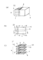
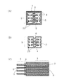
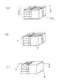
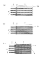
以下に、本発明の実施形態に係る固体電解コンデンサ及びその製造方法について説明する。ここで、図1(A)は、固体電解コンデンサ11の外観を示す斜視図であり、図1(B)は、固体電解コンデンサ11の外観を示す平面図であり、図1(C)は、固体電解コンデンサ11の分解斜視図である。また、図2(A)は、図1(B)の線X−Xに沿う断面図であり、図2(B)は、図1(B)の線Y−Yに沿う断面図であり、図2(C)は、図1(B)の線Z−Zに沿う断面図である。
Below, the solid electrolytic capacitor and its manufacturing method which concern on embodiment of this invention are demonstrated. Here, FIG. 1 (A) is a perspective view showing the appearance of the solid
固体電解コンデンサ11は、図1(C)に示すように、第1の主面12、第2の主面13、およびそれらを連接する側面14を有し、図1(B)、(C)に示すように絶縁層4により離間された陽極引出部2および陰極層形成部3を有している弁作用金属基体1と、4枚の弁作用金属基体が積み重ねられた積層体9を有している。
As shown in FIG. 1C, the solid
弁作用金属基体1は、例えば箔状、平板状の形態であり、材質としては、例えば、アルミニウム、タンタル、ニオブ、チタン、ジルコニウム及びこれらの合金が挙げられる。また、幅及び厚さは、製造する固体電解コンデンサ11のサイズや静電容量によって適宜選択される。
The valve
絶縁層4の構成材料は、例えばポリフェニルスルホン、ポリエーテルスルホン、シアン酸エステル樹脂、フッ素樹脂(テトラフルオロエチレン、テトラフルオロエチレン・パーフルオロアルキルビニルエーテル共重合体等)、低分子量ポリイミドや、それらの誘導体や前駆体等の絶縁性樹脂が挙げられる。特に低分子量ポリイミド、ポリエーテルスルホン、フッ素樹脂及びそれらの前駆体が好ましい。
The constituent material of the
また、図1(B)、(C)に示すように弁作用金属基体1の第1の主面12には、弁作用金属基体1の長手方向の両端面に相当する二つの側面14に端部が露出するように凹部5が形成されている。
Further, as shown in FIGS. 1B and 1C, the first
ここで、凹部5とは弁作用金属基体1の主面に対して窪んでおり、後述する導電体8を配置しうる領域を指す。
Here, the
また、図2(A)、(B)、(C)に示すように弁作用金属基体1の第1の主面12、第2の主面13、および側面14には、弁作用金属基体の酸化物からなる誘電体酸化皮膜6が形成されている。
Further, as shown in FIGS. 2A, 2B, and 2C, the first
また、図2(A)、(B)に示すように、4枚の弁作用金属基体1は、陽極引出部2および陰極層形成部3にて、接合部10を介して電気的に接合されている。(図1(C)では接合部10の表記を省略している)。
Further, as shown in FIGS. 2A and 2B, the four
また、図2(A)、(C)に示すように弁作用金属基体1の陰極層形成部3における誘電体酸化皮膜6の外表面を被覆するように固体電解質7が形成されている。具体的には、固体電解質7は、陰極層形成部3における弁作用金属基体1間の隙間、凹部5、および積層体9の外表面を被覆するように形成されている。
Further, as shown in FIGS. 2A and 2C, a
固体電解質7の材質は、例えば、チオフェン化合物、多環状スルフィド化合物、ピロール化合物、フラン化合物、アニリン化合物等を繰り返し単位として含む導電性高分子が挙げられる。
Examples of the material of the
また、図1(B)、(C)、図2(A)、(C)に示すように、弁作用金属基体1の第1の主面12における陰極層形成部3に形成された凹部5には、導電体8が充填されている。
Further, as shown in FIGS. 1B, 1 C, 2 A, and 2 C, the
また、図1(A)、図2(A)、(C)に示すように、導電体8は、弁作用金属基体1の第1の主面12における陰極層形成部3に形成された凹部5に配置されるとともに、積層体9の外表面に形成された固体電解質7を被覆するように形成されている。
Further, as shown in FIGS. 1A, 2A, and 2C, the
導電体8とは、固体電解質7に対し導電率が高いものであり、例えば銀、銅、ニッケルを含有するペースト皮膜、金属めっき皮膜が挙げられる。
The
以上のような構造の固体電解コンデンサ11では、陰極層に蓄積された電荷が、固体電解質7より導電率が高い導電体8を媒体として放出されるため、ESRを低減することができる。
In the solid
また、導電体8は、弁作用金属基体1に形成された凹部5に形成されており、弁作用金属基体1の第1の主面12から実質的に突出しておらず、この場合には、固体電解コンデンサ11の小型化の妨げとなることが無い。
Further, the
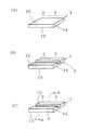
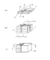
次に固体電解コンデンサ11の製造方法の一例を説明する。図3〜図5は、本発明に係る固体電解コンデンサ11の製造方法を示す斜視図である。また、図6〜図7は、本発明に係る固体電解コンデンサ11の製造方法を示す断面図である。図6(A)、(B)、(C)は、それぞれ図3(C)の線A−A、図4(A)の線B−B、図4(B)の線C1−C1およびC2−C2に沿う断面図である。また、図7(A)、(B)、(C)は、それぞれ図4(C)の線D−D、図5(A)の線E−E、図5(C)の線F−Fに沿う断面図である。以下では、図3〜図5に基づいて説明し、適宜図6〜図7を参照する。
Next, an example of a method for manufacturing the solid
まず、図3(A)に示すように、互いに対向する第1の主面12、第2の主面13、およびそれらを連接する側面14を有する箔状の弁作用金属基体1を準備する。
First, as shown in FIG. 3A, a foil-like
そして、弁作用金属基体1の長辺の一端から任意の長さの領域であって陽極端子となる領域を陽極引出部2、他端から任意の長さの領域であって容量形成部となる領域を陰極層形成部3と定義した。なお、陽極引出部2および陰極層形成部3の大きさは、固体電解コンデンサの所望の静電容量に応じて適宜設定すれば良い。
Then, a region having an arbitrary length from one end of the long side of the
ここで、弁作用金属基体1の陰極層形成部3における表面は粗面化しておくことが好ましい。このようにすることで、固体電解コンデンサ11の静電容量をより大きくすることができる。
Here, it is preferable that the surface in the cathode
次に、図3(B)に示すように、弁作用金属基体1の第1の主面12に、弁作用金属基体1の長手方向の両端面に相当する二つの側面14に露出し、弁作用金属基体1の長辺と略平行になるように凹部5を形成する。
Next, as shown in FIG. 3 (B), the first
凹部5は、プレス、スクライブ、レーザー加工などによって形成することができ、幅0.5〜2.5mm、深さ10〜25μmであることが好ましい。
The
次に、図3(C)に示すように、弁作用金属基体1の第1の主面12、第2の主面13、および側面14の表面に誘電体酸化皮膜6を形成する(図6(A)参照)。
Next, as shown in FIG. 3C, a
誘電体酸化皮膜6の形成方法は、例えば弁作用金属基体1を、リン酸、ホウ酸、アジピン酸等の電解液に浸漬し通電する陽極酸化法が挙げられる。
Examples of the method of forming the
次に、図4(A)に示すように、弁作用金属基体1の第1の主面12、第2の主面13、および側面14に、陽極引出部2および陰極層形成部3を区分するための、帯状の絶縁層4を形成する(図6(B)参照)。
Next, as shown in FIG. 4A, the
絶縁層4の形成方法は、例えば弁作用金属基体1の第1の主面12および第2の主面に、ポリフェニルスルホン、ポリエーテルスルホン、シアン酸エステル樹脂、フッ素樹脂(テトラフルオロエチレン、テトラフルオロエチレン・パーフルオロアルキルビニルエーテル共重合体等)、低分子量ポリイミドや、それらの誘導体や前駆体等の絶縁性樹脂を、弁作用金属基体1の第1の主面12、第2の主面13、および側面14に帯状に塗布した後に硬化させることが挙げられる。
The insulating
次に、図4(B)に示すように、弁作用金属基体1を4枚積み重ね、弁作用金属基体1の陽極引出部2および陰極層形成部3の所定の領域にて、接合部10によって互いに接合することに積層体9を形成する(図6(C)参照)。なお、図4(B)における、線C1に沿う断面図とC2に沿う断面図は同じ態様となる。また、図4(B)では接合部10の表記を省略している。
Next, as shown in FIG. 4 (B), four valve
弁作用金属基体1同士の接合は、例えば、所定の領域にて抵抗溶接やレーザー溶接を行い、弁作用金属基体1を溶融させる。これにより、隣接する弁作用金属基体1に由来する溶融金属同士が直接接触し、表面張力などにより一体化し、その後、溶融金属が一体化した状態で固化させることによって行うことができる。
For joining the valve
次に、積層体9を構成する弁作用金属基体1の陰極層形成領域3を、チオフェン化合物、多環状スルフィド化合物、ピロール化合物、フラン化合物、アニリン化合物等のモノマー溶液に浸漬した後に、酸化剤とドーパントの混合溶液に浸漬する操作を繰り返す。この操作によって、図4(C)に示すように、積層体9を構成する弁作用金属基体1における陰極層形成部3における誘電体酸化皮膜6の表面を被覆(すなわち、陰極層形成部3における弁作用金属基体1間の隙間および凹部5を充填し、積層体9の外表面を被覆)するように半硬化状態の固体電解質7Hが形成される。(図7(A)参照)。
Next, after immersing the cathode
ここで、弁作用金属基体1間の隙間は、表面が粗面化されている弁作用金属基体を用いている場合、単に弁作用金属基体1同士を重ね合わせるだけで、自然に形成される。
Here, when the valve action metal base | substrate with which the surface is roughened is used, the clearance gap between the valve action metal base |
次に、図5(A)に示すように、凹部5に、後述する導電体8を配置する領域を確保するために、凹部5に充填されている半硬化状態の固体電解質7Hの一部を除去する(図7(B)参照)。ここで、凹部5に充填されている半硬化状態の固体電解質7Hは、後述する固体電解質7が、凹部5において、凹部5の容積に対し20〜70%の体積となるように除去することが好ましい。
Next, as shown in FIG. 5A, a part of the semi-cured
半硬化状態の固体電解質7Hの一部を除去する方法として、例えば、弁作用金属基体1の陰極層形成部3側の側面14に露出している凹部5の端部から、流体(洗浄液、不活性気体等)14を注入し、半硬化状態の固体電解質7Hを押し出すことが挙げられる。このとき、絶縁層4の形成厚みが、陰極層形成部3に残留させる半硬化状態の固体電解質7Hの厚み以下となるように形成されていれば、流体に押し出される半硬化状態の固体電解質7Hは、弁作用金属基体1の陽極引出部側の側面14に露出している凹部5の端部より、積層体9の外部へ排出することができる。
As a method for removing a part of the semi-cured
また、弁作用金属基体1の陽極引出部に半硬化状態の固体電解質7Hが残留しないように、半硬化状態の固体電解質7Hの一部を除去した後に、弁作用金属基体1の陽極引出部を洗浄することが好ましい。
In addition, after removing a part of the semi-cured
次に、半硬化状態の固体電解質7Hを乾燥して、図5(B)に示すように固体電解質7を形成する。
Next, the semi-cured
次に、図5(C)に示すように、導電体8を、凹部5に配置するとともに積層体9の外表面に形成された固体電解質7を被覆するように形成する(図7(C)参照)。導電体8の凹部5への配置および積層体9の外表面への形成は、積層体9における固体電解質11が形成されている領域を、銀、銅、ニッケル等を含有するペースト溶液に浸漬することにより、ペースト溶液を凹部5へ浸透させるとともに積層体外部に塗布し、その後、ペースト溶液を乾燥することによって行える。
Next, as shown in FIG. 5C, the
以上のように、積層体を形成した後に、積層体を構成する弁作用金属基体に対し、固体電解質の形成および導電体の配置を一括して行うことにより、製造工程を効率化できる。 As described above, after forming the laminated body, the manufacturing process can be made more efficient by collectively forming the solid electrolyte and arranging the conductor on the valve metal substrate constituting the laminated body.
なお、導電体8は固体電解コンデンサ11の陰極として機能するため、弁作用金属基体1の陽極引出部2には形成されないようにする必要がある。
In addition, since the
以上の工程で、固体電解コンデンサ11が作製される。
The solid
なお、以上の工程を経た後に弁作用金属基体1の陽極引出部に形成された誘電体酸化皮膜を除去した後に陽極外部端子を接続し、積層体9の外表面に形成された導電体8に陰極外部端子を接続し、その後、陽極外部端子および陰極外部端子の一部が露出した状態で、積層体9をエポキシ樹脂等の絶縁樹脂で封入しても良い。
After the above steps, the dielectric oxide film formed on the anode lead portion of the
なお、上記実施形態に示した固体電解コンデンサ及びその製造方法は一例であって、これ以外にも本発明の範囲内であれば種々の変形を行うことは差し支えない。 The solid electrolytic capacitor and the manufacturing method thereof shown in the above embodiment are merely examples, and other various modifications may be made within the scope of the present invention.
弁作用金属基体の第1の主面には複数の凹部が形成されていても良く、また、第1の主面および第2の主面の双方に形成されていても良い。 A plurality of recesses may be formed on the first main surface of the valve metal substrate, or may be formed on both the first main surface and the second main surface.
弁作用金属基体の剛性を妨げない範囲で、凹部の形成数および陰極層形成部の側面における露出部の面積を多くすることにより、積層体に占める導電体の形成量および導電体の引出部が多くなり、ESRを更に低減することができる。 By increasing the number of recessed portions and the area of the exposed portion on the side surface of the cathode layer forming portion as long as the rigidity of the valve metal base is not hindered, the amount of the conductor occupying the laminate and the conductor lead-out portion can be reduced. The ESR can be further reduced.
また、弁作用金属基体の第1の主面や第2の主面における凹部の形成位置は、一端が弁作用金属基体の陰極層形成部における側面に露出している限り特に限定されず、上記実施形態に示すような、弁作用金属基体の長辺と略平行な位置関係に限定されるものではない。 Further, the formation position of the recesses on the first main surface and the second main surface of the valve action metal substrate is not particularly limited as long as one end is exposed on the side surface of the cathode layer formation portion of the valve action metal substrate. It is not limited to the positional relationship substantially parallel to the long side of the valve action metal substrate as shown in the embodiment.
また、弁作用金属基体の主面から投影した凹部の形状は、上記実施形態のように矩形であるものに限定されず、曲線部を含むような形状であっても良い。 Moreover, the shape of the recessed part projected from the main surface of the valve action metal base | substrate is not limited to what is a rectangle like the said embodiment, A shape including a curve part may be sufficient.
また、凹部の断面形状は、導電体を配置しうる形状であれば特に限定されない。 Further, the cross-sectional shape of the recess is not particularly limited as long as the conductor can be disposed.
また、積層体を構成する弁作用金属基体の全てに凹部が形成されている必要はなく、凹部が形成されている弁作用金属基体および凹部が形成されていない弁作用金属基体を併用して積層体を作製してもよい。 Further, it is not necessary that all the valve action metal bases constituting the laminate are formed with recesses, and the valve action metal base with recesses formed and the valve action metal base with no recesses are used in combination. You may make a body.
また、積層体を構成する弁作用金属基体の枚数や凹部が形成されている弁作用金属基体および凹部が形成されていない弁作用金属基体の構成比率は、固体電解コンデンサに求められる特性に応じて適宜設定することができる。 In addition, the number of valve action metal bases constituting the laminate and the composition ratio of the valve action metal bases in which recesses are formed and the valve action metal bases in which no recesses are formed depend on the characteristics required for the solid electrolytic capacitor. It can be set appropriately.
積層体を作製する際の、弁作用金属基体同士の接合位置、接合数は特に上記実施形態の接合形態に限定されるものではなく、例えば陽極引出部と陰極層形成部の一方のみに設けるようにしても良い。 The joint position and the number of joints between the valve action metal bases when producing the laminated body are not particularly limited to the joint form of the above embodiment, and for example, provided only in one of the anode lead part and the cathode layer forming part. Anyway.
また、誘電体酸化皮膜の形成は、積層体を形成した後に行っても良い。このようにすることで、弁作用金属基体同士を接合する際に、誘電体酸化皮膜を介さないため、弁作用金属基体間をより安定して接合することができる。 In addition, the dielectric oxide film may be formed after the laminate is formed. By doing in this way, when joining valve action metal bases, since a dielectric oxide film is not interposed, between valve action metal bases can be joined more stably.
また、固体電解質の形成は、電解重合や導電性高分子化合物の溶解液を塗布する方法により行っても良い。電解重合で固体電解質の形成を行う場合には、凹部
における固体電解質が所望の体積まで形成した段階で形成を停止することができるため、上記実施形態で示した、凹部における半硬化状態の固体電解質の一部を除去する操作を省略することができる。
The solid electrolyte may be formed by electrolytic polymerization or a method of applying a conductive polymer compound solution. In the case of forming a solid electrolyte by electrolytic polymerization, since the formation can be stopped at a stage where the solid electrolyte in the recess is formed to a desired volume, the semi-cured solid electrolyte in the recess shown in the above embodiment The operation of removing a part of the can be omitted.
次に本発明に係る実施例を示す。この実施例は、上記発明の実施形態に沿ったものであり、適宜図1〜図7を参照して説明する。 Next, examples according to the present invention will be described. This example is in accordance with the embodiment of the present invention, and will be described with reference to FIGS.
幅3.5mm、長さ13mm、厚さ110μmのアルミニウム箔を4枚準備した。そして、アルミニウム箔の長辺の一端から6.2mmの領域を陽極引出部と定義し、他端から6mmの領域を陰極層形成部と定義した。
Four aluminum foils having a width of 3.5 mm, a length of 13 mm, and a thickness of 110 μm were prepared. And the area | region 6.2 mm from the one end of the long side of aluminum foil was defined as the anode extraction part, and the area |
次に、このアルミニウム箔の一方主面から見て、短辺を2等分する線分を中心として幅1mm、深さ20μmの凹部を、端部がアルミニウム箔の長手方向の両端面に相当する側面に露出するように、レーザー加工によって形成した(図2(B)参照)。 Next, as viewed from one main surface of the aluminum foil, a recess having a width of 1 mm and a depth of 20 μm centering on a line segment that bisects the short side corresponds to both end surfaces in the longitudinal direction of the aluminum foil. It formed by laser processing so that it might be exposed to a side surface (refer FIG. 2 (B)).
次に、アルミニウム箔をアジピン酸アンモニウム水溶液に浸漬し、アルミニウム箔を正極側、アジピン酸アンモニウム溶液中に設置した対極を負極とし、3.5Vの電圧を印加することによって、アルミニウム箔の表面に酸化アルミニウム皮膜を形成した。 Next, the aluminum foil is immersed in an aqueous solution of ammonium adipate, the aluminum foil is used as the positive electrode, the counter electrode installed in the ammonium adipate solution is used as the negative electrode, and a voltage of 3.5 V is applied to oxidize the surface of the aluminum foil. An aluminum film was formed.
次に、アルミニウム箔の陰極層形成部おける短辺から6.4mmの位置を中心として、ポリイミド樹脂を、幅0.8mmにて、アルミニウム箔の両主面、凹部内、および側面に塗布した。そして、180℃で1時間乾燥させることによってポリイミド樹脂硬化体からなる絶縁層を形成した。(図3(A)参照)。 Next, a polyimide resin was applied to both the main surface, the concave portion, and the side surface of the aluminum foil with a width of 0.8 mm centering on the position of 6.4 mm from the short side in the cathode layer forming portion of the aluminum foil. And the insulating layer which consists of a polyimide resin hardening body was formed by making it dry at 180 degreeC for 1 hour. (See FIG. 3A).
次に、凹部、酸化アルミニウム皮膜、および絶縁層が形成されたアルミニウム箔を4枚積み重ねて積層体を作製した。 Next, four aluminum foils each having a recess, an aluminum oxide film, and an insulating layer were stacked to prepare a laminate.
そして、アルミニウム箔の主面からみて、陽極引出部および陰極層形成部の長辺を2等分する線分上において、長辺から0.5mmおよび3.0mmの位置を抵抗溶接により接合することによって積層体を作製した。 Then, the positions of 0.5 mm and 3.0 mm from the long side are joined by resistance welding on the line segment that bisects the long side of the anode lead portion and the cathode layer forming portion as viewed from the main surface of the aluminum foil. Thus, a laminate was produced.
次に、積層体を構成するアルミニウム箔における陰極層形成部を、3,4−エチレンジオキシチオフェンを含むイソプロパノール溶液に浸漬した後に、過硫酸アンモニウムとアントラキノン2スルホン酸ナトリウムの混合溶液に浸漬する操作を20回繰り返す。この操作によって、積層体を構成するアルミニウム箔における陰極層形成部に半硬化状態のポリエチレンジオキシチオフェンが形成される。 Next, an operation of immersing the cathode layer forming portion in the aluminum foil constituting the laminate in an isopropanol solution containing 3,4-ethylenedioxythiophene and then immersing in a mixed solution of ammonium persulfate and sodium anthraquinone disulfonate. Repeat 20 times. By this operation, polyethylenedioxythiophene in a semi-cured state is formed in the cathode layer forming part in the aluminum foil constituting the laminate.
次に、凹部を充填するように形成された半硬化状態のポリエチレンジオキシチオフェンに対しエアーを噴射し、後述するポリエチレンジオキシチオフェンが凹部の容積に対し20%残留するように除去した。 Next, air was sprayed on the semi-cured polyethylenedioxythiophene formed so as to fill the recess, and the later-described polyethylenedioxythiophene was removed so that 20% of the volume of the recess remained.
次に、半硬化状態のポリエチレンジオキシチオフェンが塗布された積層体をオーブン中にて乾燥することにより重合反応を進行させ、ポリエチレンジオキシチオフェンを形成した。 Next, the laminate coated with the semi-cured polyethylene dioxythiophene was dried in an oven to advance the polymerization reaction, thereby forming polyethylene dioxythiophene.
次に、積層体におけるポリエチレンジオキシチオフェンが形成された領域を、銅ペースト溶液に浸漬し、乾燥することによって、銅ペースト皮膜を、凹部に配置するとともに積層体の外表面を被覆するように銅ペースト皮膜を形成した。 Next, the region in which the polyethylene dioxythiophene is formed in the laminate is dipped in a copper paste solution and dried, so that the copper paste film is placed in the recess and the copper is coated to cover the outer surface of the laminate. A paste film was formed.
次に、アルミニウム箔の陽極引出部に陽極リードフレームを、積層体の外表面に形成された銅ペースト皮膜に陰極リードフレームを接続した。その後、リードフレームの一部が露出し、外形寸法7.3×4.3×1.9mmとなるようにエポキシ樹脂で封止することによって固体電解コンデンサを作製した。この固体電解コンデンサの体積、静電容量、体積容量効率、ESRを測定した結果を表1に示す。
(比較例1)
凹部が形成されていないアルミニウム箔を用いて、積層体を構成するアルミニウム箔間に銅ペースト皮膜を設けないようにしたこと以外は、実施例1と同様の方法で固体電解コンデンサを作製した。この固体電解コンデンサの体積、静電容量、体積容量効率、ESRを測定した結果を表1に示す。
(比較例2)
凹部が形成されていないアルミニウム箔を準備して、アルミニウム箔の表面に酸化アルミニウム皮膜を形成した。そして、アルミニウム箔の陰極層形成部に、ポリエチレンジオキシチオフェン、カーボン含有層、銀含有層を形成した後に、4枚のアルミニウム箔の陽極引出部同士を接合して積層体を作製した。
Next, the anode lead frame was connected to the anode lead portion of the aluminum foil, and the cathode lead frame was connected to the copper paste film formed on the outer surface of the laminate. Thereafter, a part of the lead frame was exposed and sealed with an epoxy resin so as to have an outer dimension of 7.3 × 4.3 × 1.9 mm, thereby producing a solid electrolytic capacitor. Table 1 shows the results of measuring the volume, capacitance, volume capacity efficiency, and ESR of this solid electrolytic capacitor.
(Comparative Example 1)
A solid electrolytic capacitor was produced in the same manner as in Example 1 except that an aluminum foil having no recess was used and no copper paste film was provided between the aluminum foils constituting the laminate. Table 1 shows the results of measuring the volume, capacitance, volume capacity efficiency, and ESR of this solid electrolytic capacitor.
(Comparative Example 2)
An aluminum foil having no recesses was prepared, and an aluminum oxide film was formed on the surface of the aluminum foil. And after forming polyethylenedioxythiophene, a carbon containing layer, and a silver containing layer in the cathode layer formation part of aluminum foil, the anode drawer parts of four aluminum foils were joined, and the laminated body was produced.
次に、アルミニウム箔の陽極引出部およびアルミニウム箔の陰極層形成部に形成された銀含有層にリードフレームを接続し、その後、リードフレームの一部が露出し、外形寸法7.3×4.3×1.9mmとなるようにエポキシ樹脂で封止することによって固体電解コンデンサを作製した。 Next, a lead frame is connected to the silver-containing layer formed in the anode lead portion of the aluminum foil and the cathode layer forming portion of the aluminum foil, and then a part of the lead frame is exposed, and the outer dimensions are 7.3 × 4. A solid electrolytic capacitor was produced by sealing with an epoxy resin so as to be 3 × 1.9 mm.
なお、アルミニウム箔の陰極層形成部へのカーボン含有層および銀含有層の形成は、酸化アルミニウム皮膜およびポリエチレンジオキシチオフェンが形成されたアルミニウム箔を、カーボンペースト溶液、銀ペースト溶液の順に浸漬して乾燥することによって行った。また、これら以外の構成は、実施例1と同様とした。 In addition, the carbon-containing layer and the silver-containing layer are formed on the cathode layer forming portion of the aluminum foil by immersing the aluminum foil in which the aluminum oxide film and the polyethylene dioxythiophene are formed in the order of the carbon paste solution and the silver paste solution. This was done by drying. Other configurations were the same as in Example 1.
この固体電解コンデンサの体積、静電容量、体積容量効率、ESRを測定した結果を表1に示す。 Table 1 shows the results of measuring the volume, capacitance, volume capacity efficiency, and ESR of this solid electrolytic capacitor.
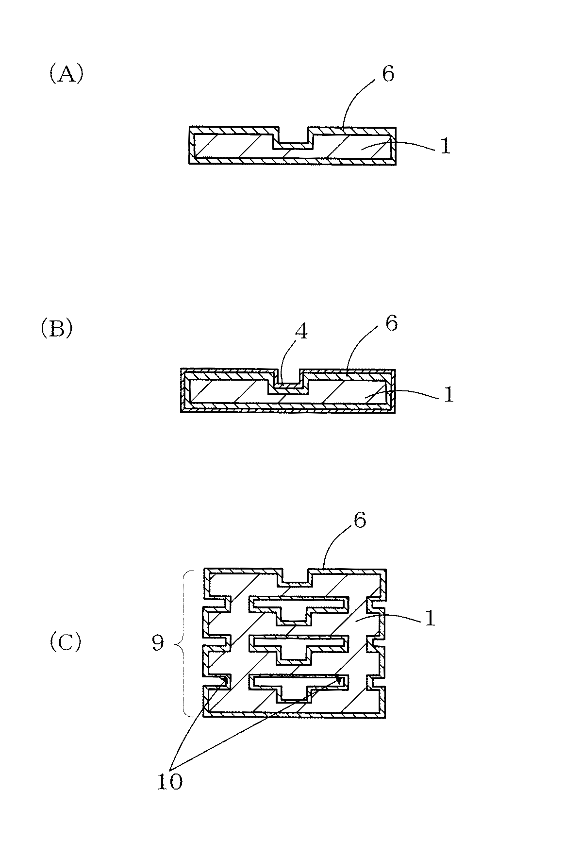
表1に示すように、本発明に係る実施例の固体電解コンデンサは、比較例1の固体電解コンデンサに対し、ESRを低減することができ、比較例2の固体電解コンデンサに対し体積容量効率を向上すなわち小型化することができた。 As shown in Table 1, the solid electrolytic capacitor of the example according to the present invention can reduce ESR with respect to the solid electrolytic capacitor of Comparative Example 1, and has a volume capacity efficiency higher than that of the solid electrolytic capacitor of Comparative Example 2. It was possible to improve or downsize.
1 弁作用金属基体
2 陽極引出部
3 陰極層形成部
4 絶縁層
5 凹部
6 誘電体酸化皮膜
7 固体電解質
7H 半硬化状態の固体電解質
8 導電体
9 積層体
10 接合部
11 固体電解コンデンサ
12 第1の主面
13 第2の主面
14 側面
DESCRIPTION OF
Claims (2)
前記弁作用金属基体の複数が積み重ねられ、陽極引出部および/または陰極層形成部にて互いに接合されてなる積層体と、
前記弁作用金属基体の少なくとも陰極層形成部における第1の主面、第2の主面、および側面に形成された誘電体酸化皮膜と、
前記弁作用金属基体の陰極層形成部における誘電体酸化皮膜を被覆するように形成された固体電解質とを備える固体電解コンデンサであって、
前記積層体を構成する少なくとも1つ以上の弁作用金属基体の、第1の主面および/または第2の主面には、少なくとも陰極層形成部を含み、少なくとも一端が前記陰極層形成部における側面に露出するように凹部が形成され、
前記弁作用金属基体の陰極層形成部における凹部には、導電体が配置されていることを特徴とする固体電解コンデンサ。 A valve metal substrate having a first main surface, a second main surface, and a side surface connecting them, and having an anode lead portion and a cathode layer forming portion;
A laminate in which a plurality of the valve action metal bases are stacked and joined to each other at the anode lead part and / or the cathode layer forming part,
A dielectric oxide film formed on at least a first main surface, a second main surface, and a side surface of at least the cathode layer forming portion of the valve action metal substrate;
A solid electrolytic capacitor comprising a solid electrolyte formed so as to cover a dielectric oxide film in a cathode layer forming portion of the valve action metal substrate,
The first main surface and / or the second main surface of at least one or more valve metal substrates constituting the laminate includes at least a cathode layer forming portion, and at least one end thereof is in the cathode layer forming portion. A recess is formed to be exposed on the side,
A solid electrolytic capacitor, wherein a conductor is disposed in a recess in the cathode layer forming portion of the valve metal substrate.
前記弁作用金属基体の複数を積み重ね、陽極引出部および/または陰極層形成部にて互いに接合する積層体形成工程であって、
前記積層体形成工程は、前記積層体を構成する少なくとも1つ以上の弁作用金属基体の、第1の主面および/または第2の主面に、少なくとも陰極層形成領域を含み少なくとも一端が前記弁作用金属基体の陰極層形成部における側面に露出するように凹部を形成する凹部形成工程と、
前記積層体を構成する弁作用金属基体の少なくとも陰極層形成部における第1の主面、第2の主面、および側面に誘電体酸化皮膜を形成する誘電体皮膜形成工程とを含み、
前記積層体形成工程の後に、前記弁作用金属基体の陰極層形成部における誘電体酸化皮膜を被覆するように固体電解質を形成する固体電解質形成工程と、
前記固体電解質形成工程の後に、前記弁作用金属基体の陰極層形成部における凹部に導電体を配置する導電体配置工程を有することを特徴とする固体電解コンデンサの製造方法。 Preparing a valve metal substrate having a first main surface, a second main surface, and a side surface connecting them, and having an anode lead portion and a cathode layer forming portion;
A stack forming step of stacking a plurality of the valve action metal bases and bonding them together at an anode lead part and / or a cathode layer forming part,
The laminated body forming step includes at least one cathode layer forming region on at least one of the first main surface and / or the second main surface of at least one valve action metal substrate constituting the laminated body. A recess forming step of forming a recess so as to be exposed on the side surface of the cathode layer forming portion of the valve action metal substrate;
A dielectric film forming step of forming a dielectric oxide film on at least the first main surface, the second main surface, and the side surface in the cathode layer forming portion of the valve metal substrate constituting the laminate,
After the laminate formation step, a solid electrolyte formation step of forming a solid electrolyte so as to cover a dielectric oxide film in the cathode layer formation portion of the valve action metal substrate,
A method for producing a solid electrolytic capacitor, comprising a conductor arranging step of arranging a conductor in a recess in a cathode layer forming portion of the valve metal substrate after the solid electrolyte forming step.
Priority Applications (1)
| Application Number | Priority Date | Filing Date | Title |
|---|---|---|---|
| JP2011050370A JP5754179B2 (en) | 2011-03-08 | 2011-03-08 | Manufacturing method of solid electrolytic capacitor |
Applications Claiming Priority (1)
| Application Number | Priority Date | Filing Date | Title |
|---|---|---|---|
| JP2011050370A JP5754179B2 (en) | 2011-03-08 | 2011-03-08 | Manufacturing method of solid electrolytic capacitor |
Publications (2)
| Publication Number | Publication Date |
|---|---|
| JP2012190819A true JP2012190819A (en) | 2012-10-04 |
| JP5754179B2 JP5754179B2 (en) | 2015-07-29 |
Family
ID=47083717
Family Applications (1)
| Application Number | Title | Priority Date | Filing Date |
|---|---|---|---|
| JP2011050370A Expired - Fee Related JP5754179B2 (en) | 2011-03-08 | 2011-03-08 | Manufacturing method of solid electrolytic capacitor |
Country Status (1)
| Country | Link |
|---|---|
| JP (1) | JP5754179B2 (en) |
Cited By (1)
| Publication number | Priority date | Publication date | Assignee | Title |
|---|---|---|---|---|
| JP2015204387A (en) * | 2014-04-15 | 2015-11-16 | パナソニックIpマネジメント株式会社 | electrolytic capacitor |
Citations (6)
| Publication number | Priority date | Publication date | Assignee | Title |
|---|---|---|---|---|
| JPS59108311A (en) * | 1982-12-13 | 1984-06-22 | 松下電器産業株式会社 | Electrode for aluminum solid electrolyde condenser |
| JPH05159988A (en) * | 1991-12-10 | 1993-06-25 | Nippon Chemicon Corp | Solid electrolytic capacitor and its manufacture |
| JPH0822932A (en) * | 1994-07-06 | 1996-01-23 | Nec Kansai Ltd | Chip solid electrolytic capacitor |
| JP2005005340A (en) * | 2003-06-10 | 2005-01-06 | Hitachi Aic Inc | Feedthrough electrolytic capacitor |
| JP2010147274A (en) * | 2008-12-19 | 2010-07-01 | Nec Tokin Corp | Solid electrolytic capacitor |
| JP2010171261A (en) * | 2009-01-23 | 2010-08-05 | Sanyo Electric Co Ltd | Solid-state electrolytic capacitor |
-
2011
- 2011-03-08 JP JP2011050370A patent/JP5754179B2/en not_active Expired - Fee Related
Patent Citations (6)
| Publication number | Priority date | Publication date | Assignee | Title |
|---|---|---|---|---|
| JPS59108311A (en) * | 1982-12-13 | 1984-06-22 | 松下電器産業株式会社 | Electrode for aluminum solid electrolyde condenser |
| JPH05159988A (en) * | 1991-12-10 | 1993-06-25 | Nippon Chemicon Corp | Solid electrolytic capacitor and its manufacture |
| JPH0822932A (en) * | 1994-07-06 | 1996-01-23 | Nec Kansai Ltd | Chip solid electrolytic capacitor |
| JP2005005340A (en) * | 2003-06-10 | 2005-01-06 | Hitachi Aic Inc | Feedthrough electrolytic capacitor |
| JP2010147274A (en) * | 2008-12-19 | 2010-07-01 | Nec Tokin Corp | Solid electrolytic capacitor |
| JP2010171261A (en) * | 2009-01-23 | 2010-08-05 | Sanyo Electric Co Ltd | Solid-state electrolytic capacitor |
Cited By (1)
| Publication number | Priority date | Publication date | Assignee | Title |
|---|---|---|---|---|
| JP2015204387A (en) * | 2014-04-15 | 2015-11-16 | パナソニックIpマネジメント株式会社 | electrolytic capacitor |
Also Published As
| Publication number | Publication date |
|---|---|
| JP5754179B2 (en) | 2015-07-29 |
Similar Documents
| Publication | Publication Date | Title |
|---|---|---|
| JP7300616B2 (en) | Electrolytic capacitor and manufacturing method thereof | |
| KR101119053B1 (en) | Solid electrolytic capacitor and method for producing solid electrolytic capacitor | |
| JP5466722B2 (en) | Solid electrolytic capacitor | |
| JP7245997B2 (en) | Electrolytic capacitor and manufacturing method thereof | |
| JP5534106B2 (en) | Solid electrolytic capacitor manufacturing method and solid electrolytic capacitor | |
| JP2003133183A (en) | Solid electrolytic capacitor and method of manufacturing the same | |
| CN101471185B (en) | Solid electrolytic capacitor with small leakage current and method for manufacturing the same | |
| CN114830275B (en) | Solid electrolytic capacitors | |
| CN108140493A (en) | Solid electrolytic capacitor and method for manufacturing solid electrolytic capacitor | |
| JP5570864B2 (en) | Solid electrolytic capacitor and manufacturing method thereof | |
| JP2015109329A (en) | Method for forming solid electrolytic capacitor | |
| KR101116120B1 (en) | Solid electrolytic capacitor element and solid electrolytic capacitor | |
| JP2008186841A (en) | Manufacturing method of solid electrolytic capacitor | |
| JP5754179B2 (en) | Manufacturing method of solid electrolytic capacitor | |
| CN103531361B (en) | Solid electrolytic capacitor And Manufacturing approach | |
| JPWO2012042950A1 (en) | Solid electrolytic capacitor and manufacturing method thereof | |
| JP2004087713A (en) | Aluminum solid electrolytic capacitors | |
| JP4899758B2 (en) | Lead frame member for solid electrolytic capacitors | |
| JP4899759B2 (en) | Lead frame member for solid electrolytic capacitors | |
| JP2007180328A (en) | Multilayer solid electrolytic capacitor and capacitor module | |
| WO2006129639A1 (en) | Solid electrolytic capacitor and method for manufacturing same | |
| JP2010147274A (en) | Solid electrolytic capacitor | |
| JP2007227716A (en) | Laminated solid electrolytic capacitor and manufacturing method therefor | |
| JP2008091390A (en) | Lead frame member for solid electrolytic capacitors | |
| JP6492424B2 (en) | Manufacturing method of solid electrolytic capacitor |
Legal Events
| Date | Code | Title | Description |
|---|---|---|---|
| A621 | Written request for application examination |
Free format text: JAPANESE INTERMEDIATE CODE: A621 Effective date: 20131213 |
|
| RD02 | Notification of acceptance of power of attorney |
Free format text: JAPANESE INTERMEDIATE CODE: A7422 Effective date: 20140110 |
|
| A977 | Report on retrieval |
Free format text: JAPANESE INTERMEDIATE CODE: A971007 Effective date: 20140821 |
|
| A131 | Notification of reasons for refusal |
Free format text: JAPANESE INTERMEDIATE CODE: A131 Effective date: 20140826 |
|
| TRDD | Decision of grant or rejection written | ||
| A01 | Written decision to grant a patent or to grant a registration (utility model) |
Free format text: JAPANESE INTERMEDIATE CODE: A01 Effective date: 20150428 |
|
| A61 | First payment of annual fees (during grant procedure) |
Free format text: JAPANESE INTERMEDIATE CODE: A61 Effective date: 20150511 |
|
| R150 | Certificate of patent or registration of utility model |
Ref document number: 5754179 Country of ref document: JP Free format text: JAPANESE INTERMEDIATE CODE: R150 |
|
| LAPS | Cancellation because of no payment of annual fees |