JP2012190820A - Housing structure of electronic apparatus - Google Patents
Housing structure of electronic apparatus Download PDFInfo
- Publication number
- JP2012190820A JP2012190820A JP2011050381A JP2011050381A JP2012190820A JP 2012190820 A JP2012190820 A JP 2012190820A JP 2011050381 A JP2011050381 A JP 2011050381A JP 2011050381 A JP2011050381 A JP 2011050381A JP 2012190820 A JP2012190820 A JP 2012190820A
- Authority
- JP
- Japan
- Prior art keywords
- claw portion
- electronic device
- case
- fitting
- claw
- Prior art date
- Legal status (The legal status is an assumption and is not a legal conclusion. Google has not performed a legal analysis and makes no representation as to the accuracy of the status listed.)
- Pending
Links
Images


Classifications
-
- H—ELECTRICITY
- H05—ELECTRIC TECHNIQUES NOT OTHERWISE PROVIDED FOR
- H05K—PRINTED CIRCUITS; CASINGS OR CONSTRUCTIONAL DETAILS OF ELECTRIC APPARATUS; MANUFACTURE OF ASSEMBLAGES OF ELECTRICAL COMPONENTS
- H05K5/00—Casings, cabinets or drawers for electric apparatus
- H05K5/10—Casings, cabinets or drawers for electric apparatus comprising several parts forming a closed casing
- H05K5/15—Casings, cabinets or drawers for electric apparatus comprising several parts forming a closed casing assembled by resilient members
Landscapes
- Engineering & Computer Science (AREA)
- Microelectronics & Electronic Packaging (AREA)
- Casings For Electric Apparatus (AREA)
- Packaging Frangible Articles (AREA)
Abstract
【課題】本発明は、少なくとも2個の部材で構成した筐体を各部材の爪部で構成している突起部で嵌合する構造において、組立性、耐落下性、耐振動性等に優れ、かつ分解が容易な嵌合構造を提供することを目的とする。
【解決手段】本発明の電子機器の筐体構造は、少なくとも第1ケースと第2ケースの2個を1または複数の爪部で嵌合する略直方体または多面体の電子機器であって、第1ケースは内側に少なくとも1つの爪部を有し、第2ケースは外向きに少なくとも1つの爪部を有し、第1ケースの爪部と第2ケースの爪部は所定の衝撃で生じる撓み量に応じて配置することを特徴とする。
【選択図】 図1The present invention has a structure in which a casing constituted by at least two members is fitted with a projection portion constituted by a claw portion of each member, and is excellent in assemblability, drop resistance, vibration resistance, and the like. An object of the present invention is to provide a fitting structure that can be easily disassembled.
A housing structure of an electronic device according to the present invention is a substantially rectangular parallelepiped or polyhedral electronic device in which at least two of a first case and a second case are fitted with one or a plurality of claws. The case has at least one claw portion on the inside, the second case has at least one claw portion outward, and the claw portion of the first case and the claw portion of the second case are bent by a predetermined impact. It arrange | positions according to.
[Selection] Figure 1
Description
本発明は、電子機器の筐体構造に関し、特に嵌合に関するものである。 The present invention relates to a housing structure of an electronic device, and particularly relates to fitting.
従来、電子機器内の各ユニットの嵌合用爪の嵌合長さを十分確保できるように大きくし、嵌合用爪をたわませることなくユニットをスライドさせる実装構造にすることにより、過度の落下衝撃等が加わっても、嵌合部が外れることがないようにしていた。(例えば、特許文献1参照。)。 Conventionally, excessive drop impact has been achieved by making the mounting structure that slides the unit without bending the fitting claws, and increasing the fitting length of the fitting claws of each unit in the electronic equipment. The fitting portion is prevented from being disengaged even when such as is added. (For example, refer to Patent Document 1).
前述の従来技術には、落下衝撃性の高い電子機器の実装構造ではあるが、分解の容易性までは考慮がなされていなかった。 Although the above-described conventional technology has a mounting structure for an electronic device having a high drop impact property, the ease of disassembly has not been considered.
本発明の電子機器の筐体構造は、少なくとも第1ケースと第2ケースの2個を1または複数の爪部で嵌合する略直方体または多面体の電子機器であって、第1ケースは内側に少なくとも1つの爪部を有し、第2ケースは外向きに少なくとも1つの爪部を有し、第1ケースの爪部と第2ケースの爪部は所定の衝撃で生じる撓み量に応じて配置することを特徴とする。 The housing structure of the electronic device according to the present invention is a substantially rectangular parallelepiped or polyhedral electronic device in which at least two of the first case and the second case are fitted with one or a plurality of claws, and the first case is on the inside. It has at least one claw part, the second case has at least one claw part facing outward, and the claw part of the first case and the claw part of the second case are arranged according to the amount of bending caused by a predetermined impact. It is characterized by doing.
また、本発明の電子機器の筐体構造は、第1ケースと第2ケースが少なくとも2つの面に少なくとも各1個の爪部を配置することを特徴とする。 The electronic device casing structure of the present invention is characterized in that the first case and the second case each have at least one claw portion disposed on at least two surfaces.
さらに、本発明の電子機器の筐体構造は、2つの面が略対向していることを特徴とする。 Furthermore, the housing structure of the electronic device of the present invention is characterized in that two surfaces are substantially opposed to each other.
さらにまた、本発明の電子機器の筐体構造は、爪部が筐体の重心に対して配置することを特徴とする。 Furthermore, the housing structure of the electronic device according to the present invention is characterized in that the claw portion is disposed with respect to the center of gravity of the housing.
また、さらに本発明の電子機器の筐体構造は、爪部が最大の撓み量の約50%の比率の位置に配置することを特徴とする。 Further, the electronic device casing structure of the present invention is characterized in that the claw portion is disposed at a position having a ratio of about 50% of the maximum deflection amount.
さらに、本発明の電子機器の筐体構造は、爪部が嵌合している面と略平行している辺の約20%から約80%の位置に配置することを特徴とする。 Furthermore, the housing structure of the electronic device according to the present invention is characterized by being arranged at a position of about 20% to about 80% of a side substantially parallel to the surface on which the claw portion is fitted.
本発明によれば、少なくとも2個の部材で構成した筐体を各部材の爪部で構成している突起部で嵌合する構造において、組立性、耐落下性、耐振動性等に優れ、かつ分解が容易な嵌合構造を提供できる。 According to the present invention, in a structure in which a casing constituted by at least two members is fitted with a protrusion constituted by a claw portion of each member, the assembly, drop resistance, vibration resistance, etc. are excellent. In addition, a fitting structure that can be easily disassembled can be provided.
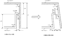
一般的な底面が開口している直方体に衝撃が加わった場合の撓みの概念について、図7を用いて説明する。図7は、底面が開口している直方体に衝撃が加わった場合の撓みの概念を説明するための説明図で、図7(A)が上カバー710の上面図であり、図7(B)が上カバー710の側面図である。
図7において、上カバー710は、長辺L1が辺x11と辺x12、短辺L3が辺y11と辺y12、高さL2で構成していて、底面が開口している直方体である。
上カバー710に衝撃等が加わった場合の撓み量は、長辺L1方向においては中央部分が最大f3maxとなり、高さL2方向においては底面方向が最大f3maxとなる。短辺L3方向においても撓みは生じるが、長辺L1方向より小である。
The concept of bending when an impact is applied to a rectangular parallelepiped having a general bottom surface will be described with reference to FIG. FIG. 7 is an explanatory diagram for explaining the concept of bending when an impact is applied to a rectangular parallelepiped whose bottom surface is open. FIG. 7 (A) is a top view of the upper cover 710, and FIG. 7 (B). FIG. 6 is a side view of the upper cover 710.
In FIG. 7, the upper cover 710 is a rectangular parallelepiped having a long side L1 constituted by a side x11 and a side x12, a short side L3 constituted by a side y11 and a side y12, and a height L2, and an open bottom.
The amount of deflection when an impact or the like is applied to the upper cover 710 is maximum f3max at the center in the direction of the long side L1, and maximum f3max in the bottom direction in the direction of the height L2. Although bending also occurs in the direction of the short side L3, it is smaller than the direction of the long side L1.
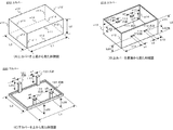
本発明による電子機器の筐体構造の一実施例について図1を用いて説明する。
図1は本発明の一実施例である電子機器の構造を示す斜視図である。図1は嵌合のための爪部を上カバー110と下カバー120に各2個配置した場合である。
図1(A)は、上カバー110を上面から見た斜視図であり、上カバー110は長辺L1、短辺L3、高さL2、底面が開口している直方体である。上面は辺x11,辺x12,辺y11,辺y12で構成している。側面は辺z11,辺z12,辺z13,辺z14で構成している。底面は辺x13,辺x14,辺y13,辺y14で構成している。
An embodiment of a housing structure of an electronic device according to the present invention will be described with reference to FIG.
FIG. 1 is a perspective view showing the structure of an electronic apparatus according to an embodiment of the present invention. FIG. 1 shows a case where two claw portions for fitting are arranged on the
FIG. 1A is a perspective view of the
図1(B)は、上カバー110を底面から見た斜視図であり、嵌合用の爪部111と爪部112を配置している。
爪部111は幅がa1であり、辺x12からL21の長さと、辺z14またはz13のb11の長さの位置に配置している。なお、b11は辺z14とz13の近い方の辺とする。
爪部112は幅がa2であり、辺x11からL22の長さと、辺z11またはz12のb12の長さの位置に配置している。なお、b12は辺z11とz12の近い方の辺とする。
FIG. 1B is a perspective view of the
The claw portion 111 has a width of a1, and is arranged at a position having a length of side x12 to L21 and a length of b11 of side z14 or z13. Note that b11 is the side closer to the sides z14 and z13.
The
図1(C)は、下カバー120を上から見た斜視図であり、下カバー120は長辺L1、短辺L3で略平板の直方体である。下カバー120は嵌合用の柱状の爪部121および爪部122を配置している。爪部121は幅がa5であり、高さがL25である。爪部122は幅がa6であり、高さがL26である。なお、爪部121および爪部122は、柱状であるため、L1方向の位置による撓み量の増減がほとんどない。
FIG. 1C is a perspective view of the lower cover 120 as viewed from above, and the lower cover 120 is a substantially flat rectangular parallelepiped having a long side L1 and a short side L3. The lower cover 120 has a columnar claw portion 121 and a
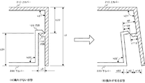
次に、上カバー110と下カバー120を嵌合した状態で所定の衝撃等が加わった場合に撓みが発生して、嵌合が外れる現象について図2を用いて説明する。図2は本発明の一実施例である電子機器の嵌合用爪部の撓みを説明するための説明図である。
図2(A)は撓みがない状態を説明するための嵌合爪部の断面図である。図2(B)は撓みが有る状態を説明するための嵌合爪部の断面図である。
Next, a phenomenon in which bending occurs when a predetermined impact or the like is applied while the
FIG. 2A is a cross-sectional view of the fitting claw portion for explaining a state where there is no deflection. FIG. 2B is a cross-sectional view of the fitting claw portion for explaining a state where there is bending.
図2(A)において、上カバー110の爪部112は下カバー120の爪部122と嵌合した状態である。上カバー110の角度k11と、下カバー120の角度k12は90°である。
図2(B)は、上カバー110と下カバー120を嵌合した状態で衝撃等が加わった場合に撓みが発生した状態を示している。
上カバー110の撓み量はc12であり、簡略的に角度で表すとk11からk11’と変化して90°より大きくなった場合である。
下カバー120の撓み量はc22であり、簡略的に角度で表すとk12からk12’と変化して90°より小さくなった場合である。
2A, the
FIG. 2B shows a state in which bending occurs when an impact or the like is applied while the
The amount of deflection of the
The amount of bending of the lower cover 120 is c22, which is a case where it is changed from k12 to k12 ′ in a simple angle and smaller than 90 °.
図2(B)において、上カバー110と下カバー120の爪部が嵌合している間隔がc2からd2と変化して、爪部112の奥行きc112と爪部122の奥行きc122の関係が式1を満たした場合に、嵌合が外れることになる。
d2>c112+c122 ・・・ (式1)
In FIG. 2B, the interval at which the claw portions of the
d2> c112 + c122 (Formula 1)
図2は、爪部112と爪部122の撓み量による嵌合が外れる内容について記載しているが、爪部111と爪部121の関係も同様である。
Although FIG. 2 describes the content of disengagement due to the amount of bending of the
次に、爪部の配置と撓み率の関係について図1と図3を用いて説明する。図3は本発明の一実施例である電子機器の嵌合用爪部の配置と爪部の撓み量の関係を示す図である。
図3は上カバー110の爪部112の配置における撓み比率Gの関係を示す図である。横軸がL2に対するL22の位置であり、数値の0が辺x11に接する位置であり、数値の1.0が辺x13に接する位置である。縦軸が爪部112の撓み比率を(%)で表示している。所定の衝撃等を加えた場合に、0%は撓みがないことを示し、100%は撓み量が最大となることを示している。
Next, the relationship between the arrangement of the claw portions and the deflection rate will be described with reference to FIGS. FIG. 3 is a diagram showing the relationship between the arrangement of the fitting claws and the amount of bending of the claws of an electronic apparatus according to an embodiment of the present invention.
FIG. 3 is a diagram showing the relationship of the deflection ratio G in the arrangement of the
撓み量δは式2により求めることができる。ここでWは爪部の撓みにかかる力であり、Lは爪部の位置の比率であり、Eは材質により異なる縦弾性係数であり、Iは形状により異なる断面二次モーメントである。
δ=WxL3/(3xExI) ・・・ (式2)
The amount of deflection δ can be obtained from Equation 2. Here, W is a force applied to the deflection of the claw portion, L is a ratio of the position of the claw portion, E is a longitudinal elastic modulus that varies depending on the material, and I is a cross-sectional secondary moment that varies depending on the shape.
δ = WxL 3 / (3xExI) (Formula 2)
図3は、撓み比率の一例として式2のL3のみを使用してb12/L1=0.5即ち図1のL1の中央位置における撓み比率を表したグラフである。L1の中央位置は撓み量δが最大(f3max)となることから、この中央位置を1とした時の長さ方向の比率pを式3から求めることができる。
p=1−2x|0.5−b12/L1| ・・・ (式3)
Figure 3 is a graph showing the percentage deflection at L1 center of b12 / L1 = 0.5 That is, FIG. 1 using only L 3 of formula 2 as an example of the ratio deflection. Since the deflection amount δ is maximum (f3max) at the center position of L1, the ratio p in the length direction when this center position is set to 1 can be obtained from Equation 3.
p = 1−2x | 0.5−b12 / L1 | (Formula 3)
図3のb12/L1=0.4はL1の中央位置から左右のいずれかに20%(p=0.8)移動させた場合の撓み比率を表したグラフである。b12/L1=0.3はL1の中央位置から左右のいずれかに40%(p=0.6)移動させた場合の撓み比率gを表したグラフである。このL1の中央位置から左右のいずれかに移動させた時の総合撓み比率Gを表したグラフである。 B12 / L1 = 0.4 in FIG. 3 is a graph showing the deflection ratio when moved 20% (p = 0.8) to the left or right from the center position of L1. b12 / L1 = 0.3 is a graph showing the deflection ratio g when 40% (p = 0.6) is moved from the central position of L1 to either the left or right. It is a graph showing the total bending ratio G when it moves to either the right or left from the center position of this L1.
L2方向の位置による撓み比率gは、式4から求めることができる。
g=(L22/L2)3 ・・・ (式4)
The deflection ratio g depending on the position in the L2 direction can be obtained from Equation 4.
g = (L22 / L2) 3 (Formula 4)
L1方向の位置による撓み比率g’は、式5から求めることができる。
g’=p3 ・・・ (式5)
The deflection ratio g ′ depending on the position in the L1 direction can be obtained from Equation 5.
g ′ = p 3 (Formula 5)
図1の辺x11、辺z12、辺x13、z11で囲まれた面の総合撓み比率Gは、式6から求めることができる。
G=gxg’ ・・・ (式6)
The total deflection ratio G of the surface surrounded by the side x11, the side z12, the side x13, and z11 in FIG.
G = gxg ′ (Formula 6)
次に本発明の一実施例の詳細について図1〜図3を用いて説明する。
図1および図2において、上カバー110と下カバー120を嵌合した状態で所定の衝撃が加わった場合に、下カバー120の爪部122に撓みが発生せず、上カバー110のみに撓みが発生した場合、嵌合状態を維持できるL22を求めるための一実施例について説明する。なお、L26はL22に連動(L26=L2−L22)して増減するものとする。
Next, details of one embodiment of the present invention will be described with reference to FIGS.
In FIG. 1 and FIG. 2, when a predetermined impact is applied with the
撓みが発生した時の条件は、L1=50mm、L2=30mm、L3=40mm、爪部112の幅a2=4mm、爪部112の奥行きc122=2.0mm、c2=2.0mm、b12=23mm、最大の撓み量f3max=4.0mmとする。
上記条件から、撓み量c22=0、撓み量c12=f3max=4.0mmとなる。
The conditions when bending occurred are L1 = 50 mm, L2 = 30 mm, L3 = 40 mm,
From the above conditions, the deflection amount c22 = 0 and the deflection amount c12 = f3max = 4.0 mm.
嵌合の境界点におけるL22’を求める。嵌合の境界点においては式7が成立する。
d2=c112+c122 ・・・ (式7)
L22 ′ at the boundary point of fitting is obtained. Equation 7 is established at the mating boundary point.
d2 = c112 + c122 (Expression 7)
撓み比率g’を求める。
爪部112は幅a2=4mmがあるため、L1の中央から2mm移動した点(b12=23mm)が衝撃を加えた場合の最終的に嵌合が外れる点となる。
式3からp=約0.93となり、式6からg’=約0.8となる。
A deflection ratio g ′ is obtained.
Since the
From Equation 3, p = approximately 0.93, and from Equation 6, g ′ = approximately 0.8.
式8から爪部112の位置L22’を求める。図3から求めても良い。
L22’=(c122/(c12xg’))(1/3)xL2 ・・・ (式8)
式8から爪部112の位置L22’は、約25.6mmとなる。
The position L22 ′ of the
L22 ′ = (c122 / (c12xg ′)) (1/3) xL2 (Expression 8)
From Expression 8, the position L22 ′ of the
上述条件の衝撃等が加わった場合に、L22がL22’未満の場合は嵌合が外れることがなく、L22がL22’以上の場合は嵌合が外れることになる。 When an impact or the like under the above conditions is applied, the fitting is not released when L22 is less than L22 ', and the fitting is released when L22 is L22' or more.
次に、嵌合に余裕度を持たせるための一実施例について説明する。
嵌合の余裕度は、最大の撓み量f3maxに余裕度jを乗じる。それから上述の式を用いて計算することにより、余裕度jを考慮したL22を求めることができる。
例えば、余裕度j=5%とすると、L22は、25.2mmとなる。
余裕度jは、5%〜20%程度とする。余裕度jを大きくし過ぎると、組立性や分解性が悪くなる。
Next, an embodiment for providing a margin for fitting will be described.
The margin of fitting is obtained by multiplying the maximum deflection amount f3max by the margin j. Then, by calculating using the above formula, L22 considering the margin j can be obtained.
For example, if the margin j = 5%, L22 is 25.2 mm.
The margin j is about 5% to 20%. If the margin j is excessively increased, the assemblability and the disassembly will deteriorate.
図1および図2において、上カバー110と下カバー120を嵌合した状態で所定の衝撃等が加わった場合に、上カバー110の爪部112に撓みが発生せず、下カバー120の爪部122のみに撓みが発生した場合、嵌合状態を維持できるL26を求めるための一実施例について説明する。なお、L22はL26に連動(L22=L2−L26)して増減するものとする。
1 and 2, when a predetermined impact or the like is applied in a state where the
撓みが発生した時の条件は、L1=50mm、L2=30mm、L3=40mm、爪部122の幅a2=4mm、爪部122の奥行き2mm、c2=2mm、L26’’=15mm、最大の撓み量f3max=2.6mmとする。
上記条件から、撓み量c12=0、撓み量c22=f3max=2.6mmとなる。
The conditions when bending occurred are L1 = 50 mm, L2 = 30 mm, L3 = 40 mm,
From the above conditions, the deflection amount c12 = 0 and the deflection amount c22 = f3max = 2.6 mm.
嵌合の境界点におけるL26’を求める。嵌合の境界点においては上述の式7が成立する。
上記条件から、撓みが発生した場合の角度k12’を式9から求める。
k12’=cos−1(c22/L26’’) ・・・ (式9)
式9からk12’は、約80°なる。
L26 ′ at the fitting boundary point is obtained. The above Equation 7 is established at the fitting boundary point.
From the above conditions, the angle k12 ′ when the bending occurs is obtained from Equation 9.
k12 ′ = cos −1 (c22 / L26 ″) (Equation 9)
From Equation 9 k12 ′ is approximately 80 °.
嵌合の境界点であるL26’は、式10から求める。
L26’=c122/cos(k12’) ・・・ (式10)
式10からL26’は、約11.5mmとなる。
L26 ′, which is a fitting boundary point, is obtained from Equation 10.
L26 ′ = c122 / cos (k12 ′) (Equation 10)
From Equation 10 L26 ′ is about 11.5 mm.
上述条件で所定の衝撃等が加わった場合に、L26がL26’未満の場合は嵌合が外れることがなく、L26がL26’以上の場合は嵌合が外れることになる。 When a predetermined impact or the like is applied under the above-described conditions, the fitting is not released when L26 is less than L26 ', and the fitting is released when L26 is L26' or more.
次に、嵌合に余裕度を持たせるための一実施例について説明する。
嵌合の余裕度は、最大の撓み量f3maxに余裕度iを乗じる。それから上述の式を用いて計算することにより、余裕度iを考慮したL26を求めることができる。
例えば、余裕度i=5%とすると、L26は、約11.0mmとなる。
余裕度iは、5%〜20%程度とする。余裕度iを大きくし過ぎると、組立性や分解性が悪くなる。
Next, an embodiment for providing a margin for fitting will be described.
The margin of fitting multiplies the maximum deflection amount f3max by the margin i. Then, by calculating using the above formula, L26 in consideration of the margin i can be obtained.
For example, if the margin i = 5%, L26 is about 11.0 mm.
The margin i is about 5% to 20%. If the margin i is too large, the assemblability and the disassembly will deteriorate.
さらに、上カバー110と下カバー120を嵌合した状態で衝撃等が加わった場合に、上カバー110の爪部112と、下カバー120の爪部122の両方に撓みが発生した場合は、式3〜式10に基づいて連立方程式を作成することにより、L22とL26を求めることができる。
Furthermore, when an impact or the like is applied in a state where the
本発明による電子機器の筐体構造の他の一実施例について図4を用いて説明する。
図4は本発明の他の一実施例である電子機器の構造を示す斜視図である。図4は嵌合のための爪部を上カバー210と下カバー220に各4個配置した場合である。
図4(A)は、上カバー210を上面から見た斜視図であり、上カバー210は長辺L1、短辺L3、高さL2、底面が開口している直方体である。上面は辺x11,辺x12,辺y11,辺y12で構成している。側面は辺z11,辺z12,辺z13,辺z14で構成している。底面は辺x13,辺x14,辺y13,辺y14で構成している。
Another embodiment of the housing structure of the electronic device according to the present invention will be described with reference to FIG.
FIG. 4 is a perspective view showing the structure of an electronic apparatus according to another embodiment of the present invention. FIG. 4 shows a case where four claw portions for fitting are arranged on each of the
FIG. 4A is a perspective view of the
図4(B)は、上カバー210を底面から見た斜視図であり、嵌合用に爪部111〜爪部114の4個を配置している。爪部111は幅がa1であり、辺x12からL21の長さと、辺z14からb11の長さの位置に配置している。 爪部112は幅がa2であり、辺x11からL22の長さと、辺z11からb12の長さの位置に配置している。爪部113は幅がa3であり、辺x12からL23の長さと、辺z13からb13の長さの位置に配置している。爪部114は幅がa4であり、辺x11からL24の長さと、辺z12からb14の長さの位置に配置している。
FIG. 4B is a perspective view of the
図4(C)は、下カバー220を上から見た斜視図であり、下カバー220は長辺L1、短辺L3で略平板の直方体である。下カバー220は嵌合用の柱状の爪部121〜爪部124の4個を配置している。爪部121は幅がa5であり、高さがL25である。爪部122は幅がa6であり、高さがL26である。爪部123は幅がa7であり、高さがL27である。爪部124は幅がa8であり、高さがL28である。なお、爪部121〜爪部124は、柱状であるため、L1方向の位置による撓み量の増減がほとんどない。
FIG. 4C is a perspective view of the
次に、上カバー210と下カバー220を嵌合した状態で衝撃等が加わった場合に撓みが発生して、嵌合が外れる現象について図5を用いて説明する。図5は本発明の他の一実施例である電子機器の嵌合用爪部の撓みを説明するための説明図である。
図5(A)は撓みがない状態を説明するための嵌合爪部の断面図である。図5(B)は撓みが有る状態を説明するための嵌合爪部の断面図である。
Next, a phenomenon in which bending occurs when an impact or the like is applied while the
FIG. 5A is a cross-sectional view of the fitting claw portion for explaining a state where there is no deflection. FIG. 5B is a cross-sectional view of the fitting claw portion for explaining a state where there is bending.
図5(A)において、上カバー210の爪部112は下カバー220の爪部122と嵌合した状態である。上カバー210の角度k21と、下カバー220の角度k22は90°である。
図5(B)は、上カバー210と下カバー220を嵌合した状態で衝撃等が加わった場合に撓みが発生した状態を示している。
上カバー210の撓み量はc12であり、簡略的に角度で表すとk21からk21’と変化して90°より大きくなった場合である。
下カバー220の撓み量はc22であり、簡略的に角度で表すとk22からk22’と変化して90°より小さくなった場合である。
5A, the
FIG. 5B shows a state in which bending occurs when an impact or the like is applied while the
The amount of bending of the
The amount of bending of the
図5(B)において、上カバー210と下カバー220の爪部が嵌合している間隔がc2からd2と変化して、爪部112の奥行きc112と爪部122の奥行きc122の関係が式1を満たした場合に、嵌合が外れることになる。
In FIG. 5B, the interval between the claw portions of the
図5は、爪部112と爪部122の撓み量による嵌合が外れる内容について記載しているが、爪部111と爪部121の関係、爪部113と爪部123の関係、爪部114と爪部124の関係も同様である。
FIG. 5 describes the content of disengagement due to the amount of bending of the
次に本発明の他の一実施例の詳細について図3〜図5を用いて説明する。
図4および図5において、上カバー210と下カバー220を嵌合した状態で所定の衝撃等が加わった場合に、下カバー220の爪部122に撓みが発生せず、上カバー210のみに撓みが発生した場合、嵌合状態を維持できるL22を求めるための一実施例について説明する。なお、L26はL22に連動(L26=L2−L22)して増減するものとする。
Next, details of another embodiment of the present invention will be described with reference to FIGS.
4 and 5, when a predetermined impact or the like is applied in a state where the
撓みが発生した時の条件は、L1=50mm、L2=30mm、L3=40mm、爪部112の幅a2=4mm、爪部112の奥行きc122=2.0mm、c2=2.0mm、b12=23mm、最大の撓み量f3max=6.0mm、b12/L1=0.4(b12=20mm、p=0.8)とする。
上記条件から、撓み量c22=0、撓み量c12=f3max=6.0mmとなる。
The conditions when bending occurred are L1 = 50 mm, L2 = 30 mm, L3 = 40 mm,
From the above conditions, the deflection amount c22 = 0 and the deflection amount c12 = f3max = 6.0 mm.
次に、b12/L1=0.4(p=0.8)の位置による撓み比率g’を式5から求めると、g’=約0.51となる。 Next, when the bending ratio g ′ at the position of b12 / L1 = 0.4 (p = 0.8) is obtained from Equation 5, g ′ = about 0.51.
嵌合の境界点におけるL22’を式8から求める。
式8から爪部112の位置L22’は、約26.0mmとなる。
L22 ′ at the fitting boundary point is obtained from Equation 8.
From Expression 8, the position L22 ′ of the
上述条件で所定の衝撃等が加わった場合に、L22がL22’未満の場合は嵌合が外れることがなく、L22がL22’以上の場合は嵌合が外れることになる。
嵌合に余裕度を持たせるための一実施例については上述と同様である。
When a predetermined impact or the like is applied under the above-described conditions, the fitting is not released when L22 is less than L22 ′, and the fitting is released when L22 is L22 ′ or more.
One embodiment for providing a margin for fitting is the same as described above.
図4および図5において、上カバー210と下カバー220を嵌合した状態で所定の衝撃等が加わった場合に、上カバー210の爪部112に撓みが発生せず、下カバー220の爪部122に撓みが発生した場合は、上述の上カバー110と下カバー120を嵌合した状態で所定の衝撃等が加わった場合に、上カバー110に撓みが発生せず、下カバー120の爪部122に撓みが発生した場合と同様である。
4 and 5, when a predetermined impact or the like is applied in a state where the
また、上カバー210と下カバー220を嵌合した状態で衝撃等が加わった場合に、下カバー220の爪部122にも撓みが発生した場合は、式3〜式10に基づいて連立方程式を作成することにより、爪部112と爪部122の配置を決めることができる。
In addition, when an impact or the like is applied with the
本発明による電子機器の筐体構造の更に他の一実施例について説明する。
図1の下カバー120および図4の下カバー220は、上述において、長辺L1、短辺L3で略平板の直方体として説明したが、上カバー110および上カバー210と同じ形状とすることもできる。この場合の撓み量と爪部の配置は、上カバー110および上カバー210と同様となる。
Another embodiment of the casing structure of the electronic device according to the present invention will be described.
The lower cover 120 in FIG. 1 and the
本発明は、組立性、耐落下性、耐振動性等に優れ、かつ分解が容易な嵌合構造を提供することを目的としているため、耐落下性、耐振動性等に優れているための爪部の配置の一実施例について図4と図5を用いて説明する。
図5において、爪部112は、撓み量の50%以下になる位置に配置することが実験結果から耐落下性、耐振動性等に優れている。
The present invention aims to provide a fitting structure that is excellent in assembling, drop resistance, vibration resistance, etc. and that can be easily disassembled, and is therefore excellent in drop resistance, vibration resistance, etc. An example of the arrangement of the claw portions will be described with reference to FIGS.
In FIG. 5, it is excellent in drop resistance, vibration resistance, etc. from the experimental results that the
また、図1の爪部112、図4の爪部112と爪部114は、L1の長さに対して約20%〜約80%の位置に配置するとことが実験結果から耐落下性、耐振動性等に優れている。
Further, the experimental results show that the
図4において、爪部111と爪部113が配置している面と略対向している面の対称とする位置に爪部112と爪部114を配置することにより、耐落下性、耐振動性等が向上する。
In FIG. 4, drop resistance and vibration resistance are provided by disposing the
さらに、筐体の重心に対して、爪部111〜爪部114を配置することにより、耐落下性、耐振動性等が向上する。 Furthermore, by arranging the claw portions 111 to 114 with respect to the center of gravity of the housing, drop resistance, vibration resistance, and the like are improved.
次に、組立性の向上および分解が容易な嵌合構造について図4を用いて説明する。
爪部111〜爪部114の配置は、耐落下性、耐振動性等を重視し過ぎると組立性や分解性が悪くなる可能性があるため、組立性や分解性を考慮した配置とする。例えば、耐落下性や耐振動性等の余裕度を小さくした爪部111〜爪部114の配置とする。
Next, a fitting structure that can be easily assembled and disassembled will be described with reference to FIG.
The arrangement of the claw part 111 to the claw part 114 is made in consideration of the assembling property and the disassembling property because there is a possibility that the assembling property and the disassembling property are deteriorated when the drop resistance, the vibration resistance and the like are too important. For example, it is set as the arrangement | positioning of the nail | claw part 111-the nail | claw part 114 which made small margins, such as fall resistance and vibration resistance.
図6は、本発明の一実施例である上カバーを補強した場合の斜視図である。
図6の上カバー310は、上カバー110や上カバー210と比較して撓み量を小さくするために、筐体の内側又は外側に補強構造用のリブや突起を設けたものである。
上カバー310にリブv1〜リブv4を設けることにより、上カバー310の撓み量を小さくすることができる。このことにより、耐落下性、耐振動性等が向上する。
FIG. 6 is a perspective view when the upper cover according to the embodiment of the present invention is reinforced.
The upper cover 310 in FIG. 6 is provided with ribs or protrusions for reinforcing structures on the inner side or the outer side of the housing in order to reduce the amount of bending compared to the
By providing the ribs v1 to v4 on the upper cover 310, the amount of bending of the upper cover 310 can be reduced. This improves the drop resistance, vibration resistance, and the like.
本発明の実施例の説明では、筐体外形を直方体で説明したが、多面体でも略直方体でも本発明を適用できることは云うまでもない。
また、本発明の実施例の説明および図面では、爪部の接触部分の形状を四角形としたが、半円でも三角形でも本発明を適用できることは云うまでもない。
以上本発明について詳細に説明したが、本発明は、ここに記載された電子機器の筐体構造に限定されるものではなく、上述の式や図面の内容を適宜に組み合わせることにより、電子機器の用途に応じた最適な嵌合構造の筐体とすることができる。このため、上記以外の電子機器の筐体構造にも広く適用することができることは云うまでもない。
In the description of the embodiments of the present invention, the outer shape of the casing is described as a rectangular parallelepiped, but it goes without saying that the present invention can be applied to a polyhedron or a substantially rectangular parallelepiped.
In the description of the embodiments of the present invention and the drawings, the shape of the contact portion of the claw portion is a quadrangle, but it goes without saying that the present invention can be applied to a semicircle or a triangle.
Although the present invention has been described in detail above, the present invention is not limited to the housing structure of the electronic device described here, and by appropriately combining the above formulas and the contents of the drawings, It can be set as the housing | casing of the optimal fitting structure according to a use. For this reason, it cannot be overemphasized that it can apply widely also to the housing | casing structure of electronic devices other than the above.
110,210,310:上カバー、120,220:下カバー、111〜114,121〜124:爪部。 110, 210, 310: upper cover, 120, 220: lower cover, 111-114, 121-124: claw portion.
Claims (6)
前記第1ケースは、内側に少なくとも1つの爪部を有し、
前記第2ケースは、外向きに少なくとも1つの爪部を有し、
前記第1ケースの爪部と前記第2ケースの爪部は、所定の衝撃で生じる撓み量に応じて配置することを特徴とする電子機器の筐体構造。 In a substantially rectangular parallelepiped or polyhedral electronic device that fits at least two of the first case and the second case with one or a plurality of claws,
The first case has at least one claw portion on the inside,
The second case has at least one claw portion outwardly;
A housing structure of an electronic device, wherein the claw portion of the first case and the claw portion of the second case are arranged according to a bending amount caused by a predetermined impact.
前記第1ケースと前記第2ケースは、少なくとも2つの面に少なくとも各1個の爪部を配置することを特徴とする電子機器の筐体構造。 The housing structure of the electronic device according to claim 1,
The first case and the second case each have at least one claw portion disposed on at least two surfaces, and a housing structure for an electronic device.
前記2つの面は、略対向していることを特徴とする電子機器の筐体構造。 The housing structure of the electronic device according to claim 2,
The housing structure of an electronic device, wherein the two surfaces are substantially opposed to each other.
爪部は、筐体の重心に対して配置することを特徴とする電子機器の筐体構造。 In the housing structure of the electronic device according to claim 2 to claim 3,
A housing structure of an electronic device, wherein the claw portion is disposed with respect to the center of gravity of the housing.
爪部は、最大の撓み量の約50%の比率の位置に配置することを特徴とする電子機器の筐体構造。 In the housing structure of the electronic device according to claim 1,
The claw portion is disposed at a position at a ratio of about 50% of the maximum deflection amount.
爪部は、爪部が嵌合している面と略平行している辺の約20%から約80%の位置に配置することを特徴とする電子機器の筐体構造。 In the housing structure of the electronic device according to any one of claims 1 to 5,
2. A housing structure of an electronic device, wherein the claw portion is disposed at a position of about 20% to about 80% of a side substantially parallel to a surface to which the claw portion is fitted.
Priority Applications (3)
| Application Number | Priority Date | Filing Date | Title |
|---|---|---|---|
| JP2011050381A JP2012190820A (en) | 2011-03-08 | 2011-03-08 | Housing structure of electronic apparatus |
| PCT/JP2011/068483 WO2012120706A1 (en) | 2011-03-08 | 2011-08-13 | Casing structure of electronic device |
| CN2011203138585U CN202340348U (en) | 2011-03-08 | 2011-08-16 | Frame structure of electronic equipment |
Applications Claiming Priority (1)
| Application Number | Priority Date | Filing Date | Title |
|---|---|---|---|
| JP2011050381A JP2012190820A (en) | 2011-03-08 | 2011-03-08 | Housing structure of electronic apparatus |
Publications (1)
| Publication Number | Publication Date |
|---|---|
| JP2012190820A true JP2012190820A (en) | 2012-10-04 |
Family
ID=46489030
Family Applications (1)
| Application Number | Title | Priority Date | Filing Date |
|---|---|---|---|
| JP2011050381A Pending JP2012190820A (en) | 2011-03-08 | 2011-03-08 | Housing structure of electronic apparatus |
Country Status (3)
| Country | Link |
|---|---|
| JP (1) | JP2012190820A (en) |
| CN (1) | CN202340348U (en) |
| WO (1) | WO2012120706A1 (en) |
Cited By (1)
| Publication number | Priority date | Publication date | Assignee | Title |
|---|---|---|---|---|
| JP2023007901A (en) * | 2021-07-02 | 2023-01-19 | パナソニックIpマネジメント株式会社 | Engagement structure of housing |
Families Citing this family (1)
| Publication number | Priority date | Publication date | Assignee | Title |
|---|---|---|---|---|
| JP6191338B2 (en) * | 2013-09-04 | 2017-09-06 | ソニー株式会社 | Housing and housing parts |
Citations (9)
| Publication number | Priority date | Publication date | Assignee | Title |
|---|---|---|---|---|
| JPS59158594A (en) * | 1983-02-28 | 1984-09-08 | 株式会社村田製作所 | Shield case of high frequency device |
| JPS6144884U (en) * | 1984-08-28 | 1986-03-25 | シャープ株式会社 | Cabinet mounting device |
| JPH1154950A (en) * | 1997-05-30 | 1999-02-26 | Lucent Technol Inc | Portable device with clamshell housing |
| JP2002064284A (en) * | 2000-08-22 | 2002-02-28 | Hitachi Kokusai Electric Inc | Electronic device mounting structure |
| JP2008269743A (en) * | 2007-04-24 | 2008-11-06 | Teac Corp | Optical disk device |
| JP2009152260A (en) * | 2007-12-19 | 2009-07-09 | Meidensha Corp | Housing of electronic apparatus |
| JP2010081293A (en) * | 2008-09-26 | 2010-04-08 | Kyocera Corp | Camera module |
| JP2010147094A (en) * | 2008-12-16 | 2010-07-01 | Sony Corp | Case body |
| JP2011004029A (en) * | 2009-06-17 | 2011-01-06 | Hochiki Corp | Fixing structure of electronic apparatus |
Family Cites Families (4)
| Publication number | Priority date | Publication date | Assignee | Title |
|---|---|---|---|---|
| JPH055712Y2 (en) * | 1987-08-28 | 1993-02-15 | ||
| JPH0568850U (en) * | 1992-02-19 | 1993-09-17 | 株式会社ユニシアジェックス | Case assembly structure |
| JP4770691B2 (en) * | 2006-10-13 | 2011-09-14 | パナソニック電工株式会社 | Case mating structure |
| JP5090709B2 (en) * | 2006-10-30 | 2012-12-05 | 京セラ株式会社 | Mobile terminal and method for assembling mobile terminal |
-
2011
- 2011-03-08 JP JP2011050381A patent/JP2012190820A/en active Pending
- 2011-08-13 WO PCT/JP2011/068483 patent/WO2012120706A1/en not_active Ceased
- 2011-08-16 CN CN2011203138585U patent/CN202340348U/en not_active Expired - Fee Related
Patent Citations (9)
| Publication number | Priority date | Publication date | Assignee | Title |
|---|---|---|---|---|
| JPS59158594A (en) * | 1983-02-28 | 1984-09-08 | 株式会社村田製作所 | Shield case of high frequency device |
| JPS6144884U (en) * | 1984-08-28 | 1986-03-25 | シャープ株式会社 | Cabinet mounting device |
| JPH1154950A (en) * | 1997-05-30 | 1999-02-26 | Lucent Technol Inc | Portable device with clamshell housing |
| JP2002064284A (en) * | 2000-08-22 | 2002-02-28 | Hitachi Kokusai Electric Inc | Electronic device mounting structure |
| JP2008269743A (en) * | 2007-04-24 | 2008-11-06 | Teac Corp | Optical disk device |
| JP2009152260A (en) * | 2007-12-19 | 2009-07-09 | Meidensha Corp | Housing of electronic apparatus |
| JP2010081293A (en) * | 2008-09-26 | 2010-04-08 | Kyocera Corp | Camera module |
| JP2010147094A (en) * | 2008-12-16 | 2010-07-01 | Sony Corp | Case body |
| JP2011004029A (en) * | 2009-06-17 | 2011-01-06 | Hochiki Corp | Fixing structure of electronic apparatus |
Cited By (2)
| Publication number | Priority date | Publication date | Assignee | Title |
|---|---|---|---|---|
| JP2023007901A (en) * | 2021-07-02 | 2023-01-19 | パナソニックIpマネジメント株式会社 | Engagement structure of housing |
| JP7773829B2 (en) | 2021-07-02 | 2025-11-20 | パナソニックオートモーティブシステムズ株式会社 | Housing locking structure |
Also Published As
| Publication number | Publication date |
|---|---|
| WO2012120706A1 (en) | 2012-09-13 |
| CN202340348U (en) | 2012-07-18 |
Similar Documents
| Publication | Publication Date | Title |
|---|---|---|
| JP5943419B2 (en) | Vibration generator | |
| KR101685962B1 (en) | Vibrator | |
| US20200366177A1 (en) | Vibration generator | |
| CN102290953A (en) | Linear vibrator | |
| JP6456572B2 (en) | Automotive electronics | |
| JP2006147305A (en) | Floating connector | |
| JP6229854B2 (en) | Electronics | |
| JP4892075B2 (en) | Electronics | |
| KR101514527B1 (en) | Vibrator | |
| KR20160016732A (en) | Optical image stabilizer actuator | |
| JPWO2018163546A1 (en) | Protection member, connector with protection member, and mounting structure of protection member | |
| JP2012190820A (en) | Housing structure of electronic apparatus | |
| JPWO2014155719A1 (en) | Battery pack and electronic device | |
| KR20160057265A (en) | Camera Module | |
| KR101712849B1 (en) | Optical image stabilizer actuator | |
| JP5219313B2 (en) | Contact terminals and electronics | |
| EP3113156A1 (en) | Picture frame | |
| JP5983301B2 (en) | Electronics | |
| KR20120101800A (en) | Linear vibrator and manufacturing of thereof | |
| JP5153019B2 (en) | Electronics | |
| JP2017055271A (en) | Information processor | |
| CN215300731U (en) | Circuit board assembly, camera module and electronic equipment | |
| KR101507477B1 (en) | Actuator for camera module | |
| JP6305743B2 (en) | Piezoelectric vibration actuator | |
| JP7005159B2 (en) | Mounting member, member having it, equipment |
Legal Events
| Date | Code | Title | Description |
|---|---|---|---|
| A621 | Written request for application examination |
Free format text: JAPANESE INTERMEDIATE CODE: A621 Effective date: 20140212 |
|
| A131 | Notification of reasons for refusal |
Free format text: JAPANESE INTERMEDIATE CODE: A131 Effective date: 20141023 |
|
| A521 | Request for written amendment filed |
Free format text: JAPANESE INTERMEDIATE CODE: A523 Effective date: 20141208 |
|
| A131 | Notification of reasons for refusal |
Free format text: JAPANESE INTERMEDIATE CODE: A131 Effective date: 20150122 |
|
| A02 | Decision of refusal |
Free format text: JAPANESE INTERMEDIATE CODE: A02 Effective date: 20150528 |