JP2012191402A - Leaky coaxial cable and method of manufacturing the same - Google Patents
Leaky coaxial cable and method of manufacturing the same Download PDFInfo
- Publication number
- JP2012191402A JP2012191402A JP2011052725A JP2011052725A JP2012191402A JP 2012191402 A JP2012191402 A JP 2012191402A JP 2011052725 A JP2011052725 A JP 2011052725A JP 2011052725 A JP2011052725 A JP 2011052725A JP 2012191402 A JP2012191402 A JP 2012191402A
- Authority
- JP
- Japan
- Prior art keywords
- lcx
- cable
- outer conductor
- leakage
- conductor
- Prior art date
- Legal status (The legal status is an assumption and is not a legal conclusion. Google has not performed a legal analysis and makes no representation as to the accuracy of the status listed.)
- Pending
Links
Images




Landscapes
- Manufacturing Of Electric Cables (AREA)
- Waveguide Aerials (AREA)
Abstract
【課題】製造コストを上昇させることがなく、また、ケーブルの長さ方向について結合損失が安定化されたLCXを提供し、また、ケーブルの長さ方向について結合損失が安定化されたLCXを低廉なコストで製造することができるLCXの製造方法を提供する。
【解決手段】中心導体102と、中心導体102を被覆した絶縁体103と、絶縁体103の外側を覆う外部導体104とが同軸構造となされ、外部導体104に漏洩電磁界形成用の複数のスロット部101が形成され、外部導体104が外被105で覆われた漏洩同軸ケーブルであって、外部導体104は、スロット部101となる開孔の形状がレジストインクにより印刷されて固着され金属を腐食させる液中に通過されることにより開孔が形成された金属テープが、絶縁体103の外周面に巻付けられて構成されたものである。
【選択図】図6An object of the present invention is to provide an LCX in which the coupling loss is stabilized in the cable length direction without increasing the manufacturing cost, and the LCX in which the coupling loss is stabilized in the cable length direction. An LCX manufacturing method that can be manufactured at a low cost is provided.
A center conductor, an insulator covering the center conductor, and an outer conductor covering the outside of the insulator have a coaxial structure, and the outer conductor has a plurality of slots for forming a leakage electromagnetic field. A leaky coaxial cable in which a portion 101 is formed and an outer conductor 104 is covered with a jacket 105. The outer conductor 104 is printed with resist ink to fix the shape of the hole that becomes the slot portion 101 and corrodes the metal. A metal tape having an opening formed by being passed through the liquid to be wound is configured to be wound around the outer peripheral surface of the insulator 103.
[Selection] Figure 6
Description
本発明は、漏洩同軸ケーブル及び漏洩同軸ケーブルの製造方法に関し、特に、スロット部の加工が容易化され、また、結合損失が安定化された漏洩同軸ケーブル及び漏洩同軸ケーブルの製造方法に関するものである。 The present invention relates to a leaky coaxial cable and a leaky coaxial cable manufacturing method, and more particularly to a leaky coaxial cable and a leaky coaxial cable manufacturing method in which processing of a slot portion is facilitated and coupling loss is stabilized. .
漏洩同軸ケーブル(以下、「LCX」という。)は、図6に示すように、内部導体102、絶縁体103、外部導体104及び外被(シース)105を備えて同軸状に構成されている。このLCXは、従来より、新幹線沿いに布設されて列車と地上との無線連絡のために使用されたり、あるいは、地下鉄構内や地下街に布設されて地上との消防無線や警察無線の連絡用に使用されている。このようなLCX1においては、同軸内部の電磁エネルギーを外部に漏洩させるために、外部導体104上に周期的なスロット部101が設けられている。
As shown in FIG. 6, the leaky coaxial cable (hereinafter referred to as “LCX”) includes an inner conductor 102, an insulator 103, an outer conductor 104, and a jacket (sheath) 105 and is configured in a coaxial shape. Conventionally, this LCX is installed along the Shinkansen and used for wireless communication between the train and the ground, or it is installed in the subway yard and underground mall and used for communication between the ground and fire and radio. Has been. In such an
すなわち、LCX1の外部導体104には、ケーブル軸に対して一定周期毎に、一周期当たり複数の長孔状のスロット部101が設けられている。各スロット部101は、ケーブル軸に対していくらかの角度を持って傾斜されている。なお、各スロット部101の間隔の半分が使用周波数の半波長と一致したり、その半波長の整数倍となったときには、共振状態となる。この周波数を共振周波数と呼ぶ。
That is, the outer conductor 104 of the
このようなLCXを製造するには、まず、内部導体102の周囲に円柱状の絶縁体103を形成する。内部導体102は、絶縁体103の中心軸に沿って挿通された状態となる。次に、絶縁体103の外周面に、金属テープを縦添え状に巻き付ける。この金属テープには、スロット部101となる開孔が設けられている。この金属テープは、外部導体104となる。そして、この外部導体104上に外被105を形成することにより、LCXが完成する。 In order to manufacture such an LCX, first, a cylindrical insulator 103 is formed around the inner conductor 102. The inner conductor 102 is inserted along the central axis of the insulator 103. Next, a metal tape is wound around the outer peripheral surface of the insulator 103 in a vertically attached shape. The metal tape is provided with an opening that becomes the slot portion 101. This metal tape becomes the outer conductor 104. Then, by forming the jacket 105 on the outer conductor 104, the LCX is completed.
特許文献1には、外部導体104となる金属テープに、金型を用いた打ち抜き法で開孔を作製することが記載されている。特許文献2には、外部導体104となる金属テープに、エンドミルを用いた切削法で開孔を作製することが記載されている。また、特許文献3には、外部導体104となる金属テープに、レーザ光で開孔を作製することが記載されている。そして、特許文献4には、外部導体104となる金属テープに、エッチング法で開孔を作製することが記載されている。
また、LCXにおいては、結合損失をケーブルの長さ方向について安定化させることが要請されている。結合損失を安定化させるためには、非特許文献1に記載されているように、スロット部101からの放射効率を変化させればよい。この技術は、一般にグレーディングと呼ばれている。すなわち、LCXとの間隔を一定に保ちながらアンテナを移動させると、アンテナが給電側から遠ざかるにつれて、LCXの伝送損失のために、アンテナの受信電力は減少する。これを防止するために、結合損失の異なるLCXを組み合わせて、その伝送損失を補償するように、給電側から遠い部分に結合損失の小さな(電磁波漏洩量の多い)LCXを使用すれば、同一の結合損失を有するLCXのみで構成するよりも長く、かつ、受信レベル変動幅の小さい通信システムを構成することができる。非特許文献1には、結合損失の異なる3種類のLCXを使用した例が記載されている。結合損失を変化させるためには、スロット部101の形状(大きさ、太さ、角度など)を変化させる必要がある。
In LCX, it is required to stabilize the coupling loss in the cable length direction. In order to stabilize the coupling loss, the radiation efficiency from the slot portion 101 may be changed as described in Non-Patent
ところで、前述したように、外部導体104となる金属テープに金型を用いた打ち抜き法で開孔を作製する場合には、金型の製作費が高価であるという問題がある。また、打ち抜き回数が増加するにしたがって金型が磨耗するため、金型を交換する必要が生じ、生産コスト上昇が招来される。また、金型の形状によって決まる同一形状、あるいは、数種類の金型による数種類の形状の開孔しか作製できないという問題がある。 By the way, as described above, when an opening is formed by a punching method using a mold on a metal tape to be the outer conductor 104, there is a problem that the manufacturing cost of the mold is expensive. Further, since the mold is worn as the number of punches increases, it is necessary to replace the mold, resulting in an increase in production cost. In addition, there is a problem that only the same shape determined by the shape of the mold or several types of shapes of holes can be produced.
外部導体104となる金属テープにエンドミルを用いた切削法で開孔を作製する場合には、加工時間が長いという問題がある。また、切削時間が増加するにしたがってエンドミルが磨耗するため、エンドミルを交換する必要が生じ、生産コスト上昇が招来される。 There is a problem in that the processing time is long when the hole is formed in the metal tape to be the outer conductor 104 by a cutting method using an end mill. Moreover, since the end mill wears as the cutting time increases, it is necessary to replace the end mill, resulting in an increase in production cost.
また、外部導体104となる金属テープに、レーザ光で開孔を作製する場合には、レーザ照射装置が、例えば1億円程度と極めて高額であるという問題がある。そのために、製品コストが大幅に上昇してしまう。 Further, when a hole is formed in the metal tape to be the outer conductor 104 with a laser beam, there is a problem that the laser irradiation apparatus is extremely expensive, for example, about 100 million yen. As a result, the product cost increases significantly.
そして、外部導体104となる金属テープに、エッチング法で開孔を作製する場合には、工程が複雑であるため、製品コストが上昇してしまうという問題がある。また、フォトマスクを高精度に作製しなければならず、フォトマスクの配置にも高い精度が要求されるため、製造コストの上昇を招いていた。すなわち、図7に示すように、フォトエッチングでは、まず、LCXの外部導体となる金属テープの全面にレジストを塗布する(ステップst101)。そして、別に製作したフォトマスク用の開孔パターン原版(ステップst102〜st103)を、レジストを塗布した金属テープ上に高精度に配置し(ステップst104)、パターン原版の上から露光して必要な金属部分のみを焼付けて固着させる(ステップst105)。その後、現像を行い、開孔になる部分のレジストを除去して(ステップst106)、エッチングによって開孔となる部分の金属体を腐食液によって溶かして除去する(ステップst107)という工程が必要である。また、不要なレジストは除去される(ステップst108)ため、レジスト材料の損失による資源の浪費が生ずる。 And when producing an opening by the etching method in the metal tape used as the external conductor 104, since a process is complicated, there exists a problem that product cost will rise. In addition, since the photomask has to be manufactured with high accuracy and high accuracy is required for the arrangement of the photomask, the manufacturing cost has been increased. That is, as shown in FIG. 7, in the photoetching, first, a resist is applied to the entire surface of the metal tape to be the outer conductor of the LCX (step st101). Then, a separately prepared photomask aperture pattern master (steps st102 to st103) for photomask is arranged with high precision on a metal tape coated with a resist (step st104) and exposed from above the pattern master to obtain the necessary metal. Only the portion is baked and fixed (step st105). Thereafter, development is performed to remove the resist in the part that becomes the opening (step st106), and the metal part in the part that becomes the opening is removed by etching with a corrosive solution (step st107). . Further, unnecessary resist is removed (step st108), so that resources are wasted due to loss of resist material.
そして、結合損失の異なるLCXを接続することによる結合損失の安定化においては、結合損失は、LCXの長さ方向に鋸状に10dB程度の変化がある。これでは、一定の結合損失のLCXのみを用いた場合よりは結合損失は安定化しているものの、完全な安定化ではない。そのため、LCXと、LCXの周囲に存在する通信相手となる無線移動端末との間において、通信速度の低下が生ずる虞があり、また、結合損失の大きい場所において、LCXと無線移動端末との間に電波障害物が入った場合には、結合損失が急激に増加して通信不能となる虞がある。 In the stabilization of the coupling loss by connecting LCXs having different coupling losses, the coupling loss changes in a sawtooth shape in the length direction of the LCX by about 10 dB. In this case, although the coupling loss is stabilized as compared with the case where only LCX having a constant coupling loss is used, it is not complete stabilization. Therefore, there is a possibility that the communication speed may be reduced between the LCX and a wireless mobile terminal that is a communication partner existing around the LCX, and between the LCX and the wireless mobile terminal in a place where the coupling loss is large. If a radio wave obstruction enters into the antenna, the coupling loss may increase rapidly and communication may become impossible.
また、結合損失の異なるLCXを接続するためには、多くの種類のLCXをいくつも布設現場に輸送しなければならず、また、LCXの接続のためにコネクタを必要とするので、コネクタの費用や取り付け作業も必要となる。したがって、このような結合損失の安定化技術においては、輸送費、材料費、工事費等のコストの上昇が招来される。 In addition, in order to connect LCXs with different coupling losses, many types of LCXs must be transported to the installation site, and connectors are required for LCX connections. And installation work is also required. Therefore, such a coupling loss stabilization technique causes an increase in costs such as transportation costs, material costs, and construction costs.
そこで、本発明は、前述の実情に鑑みて提案されるものであり、その目的は、製造コストを上昇させることがなく、また、ケーブルの長さ方向について結合損失が安定化されたLCXを提供し、また、ケーブルの長さ方向について結合損失が安定化されたLCXを低廉なコストで製造することができるLCXの製造方法を提供することにある。 Accordingly, the present invention has been proposed in view of the above-described circumstances, and its purpose is to provide an LCX that does not increase the manufacturing cost and has a stable coupling loss in the cable length direction. Another object of the present invention is to provide an LCX manufacturing method capable of manufacturing an LCX whose coupling loss is stabilized in the cable length direction at a low cost.
前述の課題を解決し、前記目的を達成するため、本発明に係るLCXは、以下の構成のいずれか一を有するものである。 In order to solve the above-described problems and achieve the above object, the LCX according to the present invention has any one of the following configurations.
〔構成1〕
中心導体と中心導体を被覆した絶縁体と絶縁体の外側を覆う外部導体とが同軸構造となされ外部導体に漏洩電磁界形成用の複数のスロット部が形成され外部導体が外被で覆われた漏洩同軸ケーブルであって、外部導体は、スロット部となる開孔の形状がレジストインクにより印刷されて固着された後金属を腐食させる液中に通過されることにより開孔が形成された金属テープが、絶縁体の外周面に巻付けられて構成されたものであることを特徴とするものである。
[Configuration 1]
The center conductor, the insulator covering the center conductor, and the outer conductor covering the outside of the insulator have a coaxial structure, and a plurality of slots for forming a leakage electromagnetic field are formed in the outer conductor, and the outer conductor is covered with a jacket. A leaky coaxial cable, in which the outer conductor is a metal tape in which the shape of the opening serving as the slot portion is printed with a resist ink and fixed, and then passed through a liquid that corrodes the metal. Is formed by being wound around the outer peripheral surface of the insulator.
〔構成2〕
構成1を有する漏洩同軸ケーブルにおいて、スロット部からの漏洩電磁界の漏洩量が、ケーブルの全長に渡って連続的に変化していることを特徴とするものである。
[Configuration 2]
The leaky coaxial cable having the
〔構成3〕
構成1、または、構成2を有する漏洩同軸ケーブルにおいて、スロット部の形状がケーブル長さ方向について連続的に変化しており、漏洩電磁界の漏洩量がケーブル長さ方向について給電側から離れるにしたがって連続的に増加し、ケーブル長さ方向についての漏洩電磁界の大きさの変化が抑えられていることを特徴とするものである。
[Configuration 3]
In the leaky coaxial cable having the
〔構成4〕
構成3を有する漏洩同軸ケーブルにおいて、ケーブル長が、ケーブル長さ方向について給電側から離れるにしたがって連続的に増加する漏洩電磁界の漏洩量が急激に増加する距離に相当する長さ以下となっていることを特徴とするものである。
[Configuration 4]
In the leaky coaxial cable having the
〔構成5〕
構成1を有する漏洩同軸ケーブルにおいて、ケーブルの減衰量が、所望の箇所において選択的に変化していることを特徴とするものである。
[Configuration 5]
The leaky coaxial cable having the
また、本発明に係るLCXの製造方法は、以下の構成を有するものである。 Moreover, the manufacturing method of LCX which concerns on this invention has the following structures.
〔構成6〕
中心導体を絶縁体により被覆する工程と、金属テープに漏洩電磁界形成用の複数のスロット部となる開孔の形状をレジストインクにより印刷して固着させる工程と、金属テープを金属を腐食させる液中に通過させ該金属テープに開孔を形成する工程と、金属テープを絶縁体の外周面に巻付けて外部導体とする工程と、外部導体を外被で覆う工程とを有することを特徴とするものである。
[Configuration 6]
A step of covering the central conductor with an insulator, a step of printing and fixing the shape of the openings serving as a plurality of slot portions for forming a leakage electromagnetic field on the metal tape with a resist ink, and a solution for corroding the metal tape with the metal. A step of forming an opening in the metal tape by passing it through, a step of winding the metal tape around the outer peripheral surface of the insulator to form an external conductor, and a step of covering the external conductor with a jacket To do.
構成1を有する本発明に係るLCXにおいては、外部導体は、スロット部となる開孔の形状がレジストインクにより印刷されて固着された後金属を腐食させる液中に通過されることにより開孔が形成された金属テープが、絶縁体の外周面に巻付けられて構成されたものであるので、製造コストが抑えられている。
In the LCX according to the present invention having the
構成2を有する本発明に係るLCXにおいては、スロット部からの漏洩電磁界の漏洩量がケーブルの全長に渡って連続的に変化しているので、ケーブルの長さ方向について結合損失を安定化させることができる。
In the LCX according to the present invention having the
構成3を有する本発明に係るLCXにおいては、スロット部の形状がケーブル長さ方向について連続的に変化しており、漏洩電磁界の漏洩量がケーブル長さ方向について給電側から離れるにしたがって連続的に増加し、ケーブル長さ方向についての漏洩電磁界の大きさの変化が抑えられているので、ケーブルの長さ方向について結合損失を安定化させることができる。
In the LCX according to the present invention having the
構成4を有する本発明に係るLCXにおいては、ケーブル長が、ケーブル長さ方向について給電側から離れるにしたがって連続的に増加する漏洩電磁界の漏洩量が急激に増加する距離に相当する長さ以下となっているので、ケーブルの長さ方向について結合損失を安定化させることができる。
In the LCX according to the present invention having the
構成5を有する本発明に係るLCXにおいては、ケーブルの減衰量が、所望の箇所において選択的に変化しているので、ケーブルの長さ方向について結合損失を所望の状態とすることができる。
In the LCX according to the present invention having the
構成6を有する本発明に係るLCXの製造方法においては、金属テープに漏洩電磁界形成用の複数のスロット部となる開孔の形状をレジストインクにより印刷して固着させ、この金属テープを金属を腐食させる液中に通過させ該金属テープに開孔を形成し、この金属テープを絶縁体の外周面に巻付けて外部導体とするので、ケーブルの長さ方向について結合損失が安定化されたLCXを低廉なコストで製造することができる。 In the LCX manufacturing method according to the present invention having the configuration 6, the shape of the openings serving as the plurality of slot portions for forming the leakage electromagnetic field is fixed on the metal tape by printing with resist ink, and the metal tape is attached to the metal tape. An opening is formed in the metal tape by passing it through the corrosive liquid, and this metal tape is wound around the outer peripheral surface of the insulator to form an outer conductor, so that the coupling loss is stabilized in the cable length direction. Can be manufactured at low cost.
すなわち、本発明は、製造コストを上昇させることがなく、また、ケーブルの長さ方向について結合損失が安定化されたLCXを提供し、また、ケーブルの長さ方向について結合損失が安定化されたLCXを低廉なコストで製造することができるLCXの製造方法を提供することができるものである。 That is, the present invention provides an LCX in which the manufacturing loss is not increased, the coupling loss is stabilized in the cable length direction, and the coupling loss is stabilized in the cable length direction. It is possible to provide a method for manufacturing LCX that can manufacture LCX at low cost.
以下、本発明を実施するための形態について図面を参照して説明する。 Hereinafter, embodiments for carrying out the present invention will be described with reference to the drawings.
図6は、LCXの構成を示す側面図である。 FIG. 6 is a side view showing the configuration of the LCX.
本発明に係るLCXの製造方法により製造されるLCXは、図6に示すように、内部導体102、絶縁体103、外部導体104及び外被(シース)105が同軸状に構成されたものである。このLCX1においては、同軸内部の電磁エネルギーを外部に漏洩させるために、外部導体104上に周期的なスロット部101が設けられている。スロット部101は、外部導体104に、ケーブル軸に対して一定周期毎に設けられている。各スロット部101は、ケーブル軸に対していくらかの角度を持って傾斜されている。
As shown in FIG. 6, the LCX manufactured by the LCX manufacturing method according to the present invention has an inner conductor 102, an insulator 103, an outer conductor 104, and a jacket (sheath) 105 configured in a coaxial manner. . In this
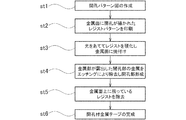
図1は、本発明に係るLCXの製造方法を示すフローチャートである。 FIG. 1 is a flowchart showing a method for manufacturing LCX according to the present invention.
本発明においては、図1に示すように、外部導体104にスロット部101となる開孔を形成するために、エッチング法を使用する。すなわち、レジストインクを、目的とする開孔パターンにしたがって外部導体104となる金属テープに印刷する。すなわち、ステップst1で、開孔パターン図を作製しておく。 In the present invention, as shown in FIG. 1, an etching method is used to form an opening serving as the slot portion 101 in the outer conductor 104. That is, the resist ink is printed on the metal tape that becomes the external conductor 104 in accordance with the target hole pattern. That is, an opening pattern diagram is prepared in step st1.
図2は、本発明に係るLCXの外部導体の構成を示す側面図である。 FIG. 2 is a side view showing the configuration of the outer conductor of the LCX according to the present invention.
次に、ステップst2で、図2に示すように、外部導体104となる金属テープに、開孔101が描かれたレジストパターンをレジストインク106により印刷する。このとき、開孔101の描かれたレジストパターンを金属テープに直接印刷するので、高精度のフォトマスクを作製する必要は無く、また、フォトマスクをレジスト面に高精度に配置する必要も無い。また、印刷は、インクジェットプリンタによって行うことができるので安価に行うことができる。 Next, in step st <b> 2, as shown in FIG. 2, a resist pattern in which the opening 101 is drawn is printed on the metal tape to be the outer conductor 104 with the resist ink 106. At this time, since the resist pattern in which the opening 101 is drawn is directly printed on the metal tape, it is not necessary to manufacture a high-precision photomask and it is not necessary to arrange the photomask on the resist surface with high accuracy. Moreover, since printing can be performed by an inkjet printer, it can be performed at low cost.
さらに、レジストインク106は、開孔101となる部分を除いた領域のみに印刷(塗布)される。従来の製造方法では、金属テープの全面にレジストを塗布し、露光されない部分(開孔101となる部分)のレジストは、余分なレジストとして除去されていた。本発明においては、開孔101となる部分に余分にレジストインク106が印刷(塗布)されることがないので、資源の節約になる。 Further, the resist ink 106 is printed (applied) only in a region excluding a portion that becomes the opening 101. In the conventional manufacturing method, a resist is applied to the entire surface of the metal tape, and the resist in the portion that is not exposed (portion that becomes the opening 101) is removed as an extra resist. In the present invention, since the resist ink 106 is not printed (applied) excessively on the portion to be the opening 101, resources are saved.
ここで用いるレジストインクとしては、特開2009−35700号公報に記載されたチッソ株式会社製のものや、特開2010−53177号公報に記載された東京インキ株式会社製のものなどを使用することができる。 As resist ink used here, the thing made by Chisso Corporation described in Unexamined-Japanese-Patent No. 2009-35700, the thing made by Tokyo Ink Corporation described in Unexamined-Japanese-Patent No. 2010-53177, etc. should be used. Can do.
そして、図1に示すように、ステップst3において、レジストパターンに露光し、レジストインクを硬化させて金属テープに焼き付ける。ステップst4において、金属部が露出した開孔となる箇所の金属を、エッチングにより除去して、開孔を形成する。ステップst5において、金属テープ上に残っているレジストインクを除去する。ステップst6において、開孔が形成された金属テープが完成する。この金属テープを、絶縁体103上に縦添えにして巻き付けて、外部導体104とする。 Then, as shown in FIG. 1, in step st3, the resist pattern is exposed, the resist ink is cured and baked on a metal tape. In step st4, the metal in the portion that becomes the opening where the metal portion is exposed is removed by etching to form the opening. In step st5, the resist ink remaining on the metal tape is removed. In step st6, the metal tape in which the holes are formed is completed. This metal tape is wound vertically on the insulator 103 to form the outer conductor 104.
そして、本発明に係るLCXの製造方法においては、図2に示すように、前述のようにして形成するスロット部101の形状をケーブルの長さ方向について連続的に変化させ、すなわち、連続グレーディングを行うことにより、結合損失を段階的ではなく連続的に変化させ、受信レベルの変動幅を極限まで小さくすることができる。 In the LCX manufacturing method according to the present invention, as shown in FIG. 2, the shape of the slot portion 101 formed as described above is continuously changed in the cable length direction, that is, continuous grading is performed. By doing so, the coupling loss can be continuously changed instead of stepwise, and the fluctuation range of the reception level can be minimized.
すなわち、スロット部101となる開孔を前述したように作製することにより、開孔の形状を、複雑に変化させることができる。開孔の形状を微妙に変化させることにより、このLCXにおける結合損失が、ケーブル長さ方向ついて一定とすることができる。形状が微妙に変化する開孔のパターンは、CAD等により作図することができ、そのデータをコンピュータ装置に取り込んで、インクジェットプリンタにより、レジストインクを金属テープに直接印刷することができる。そして、エッチング工程により、開孔となる部分の金属を除去すれば、ケーブル長さ方向について微妙に形状が変化する開孔を形成することができる。 In other words, the shape of the opening can be changed in a complicated manner by making the opening to be the slot portion 101 as described above. By slightly changing the shape of the opening, the coupling loss in the LCX can be made constant in the cable length direction. A pattern of apertures whose shape changes slightly can be drawn by CAD or the like, and the data can be taken into a computer device and resist ink can be directly printed on a metal tape by an ink jet printer. And if the metal of the part used as an opening is removed by an etching process, the opening which a shape changes delicately about a cable length direction can be formed.
また、このLCXの製造方法においては、開孔の形状を自在に変化させることができるので、漏洩電磁界の漏洩量を、所望の箇所において選択的に変化させることもできる。 Further, in this LCX manufacturing method, the shape of the opening can be freely changed, so that the leakage amount of the leakage electromagnetic field can be selectively changed at a desired location.
本発明の実施例として、外径2mmの円柱状の銅線を中心導体として、LCXを作製した。中心導体上には、発泡ポリエチレン絶縁体を押出し成形で構成し、この発泡ポリエチレン絶縁体により、外径5mmの絶縁体を形成した。 As an example of the present invention, an LCX was produced using a cylindrical copper wire having an outer diameter of 2 mm as a central conductor. A foamed polyethylene insulator was formed by extrusion molding on the center conductor, and an insulator having an outer diameter of 5 mm was formed from the foamed polyethylene insulator.
次に、外部導体として、幅20mmのプラスチックテープ付銅テープを50m用意した。プラスチックテープ付銅テープは、厚さ0.01mmの銅テープに、強度向上のために厚さ0.06mmのプラスチックテープを貼り合わせたものであって、厚さは、0.07mmである。 Next, 50 m of a copper tape with a plastic tape having a width of 20 mm was prepared as an external conductor. The copper tape with plastic tape is obtained by bonding a plastic tape with a thickness of 0.06 mm to a copper tape with a thickness of 0.01 mm for the purpose of improving the strength, and the thickness is 0.07 mm.
このプラスチックテープ付銅テープの銅テープ側に、光で固着するレジストインクを用いて、インクジェットプリンタにより開孔が描かれたレジストパターンを印刷して固着させた。そして、エッチングにより、スロット部となる開孔を形成した。この外部導体を、絶縁体上に縦添えして巻き付けた。 On the copper tape side of the copper tape with plastic tape, a resist pattern in which apertures were drawn was printed and fixed using a resist ink that was fixed by light. And the opening used as a slot part was formed by the etching. This outer conductor was wound vertically on an insulator.
さらに、外部導体上に、厚さ0.75mmの難燃ノンハロゲンポリエチレン樹脂を押出し成形し、この難燃ノンハロゲンポリエチレン樹脂により、外径約7mmの外被を形成した。なお、外径が約7mmとなるのは、絶縁体と外部導体との間、または、外部導体と外被との間に、若干の空気層が形成されるためである。 Further, a flame-retardant non-halogen polyethylene resin having a thickness of 0.75 mm was extruded on the outer conductor, and a jacket having an outer diameter of about 7 mm was formed from the flame-retardant non-halogen polyethylene resin. The reason why the outer diameter is about 7 mm is that a slight air layer is formed between the insulator and the outer conductor or between the outer conductor and the jacket.
このLCXの目標とする特性は、LCXから1.5m離れた地点での結合損失が80dBで、ケーブル長さ方向について一定であることとした。 The target characteristic of this LCX is that the coupling loss at a point 1.5 m away from the LCX is 80 dB and is constant in the cable length direction.
銅テープに印刷した開孔が描かれたレジストパターンは、図2に示すように、位置0mでは、LCXから1.5m離れた場所で80dBの結合損失を得るために、長さ7mm、幅2mmの細長い開孔をケーブル軸に対する角度が20度のジグザグ状に形成した。位置23mでは、1.5m離れた場所で80dBの結合損失を得るために、23m分の減衰量を補償するためにLCXの結合損失を70dBにする必要があるので、細長い開孔の形状は、長さ12mm、幅2mm、ケーブル軸に対する角度を20度とした。
As shown in FIG. 2, the resist pattern on which the opening printed on the copper tape is drawn has a length of 7 mm and a width of 2 mm in order to obtain a coupling loss of 80 dB at a position 1.5 m away from the LCX at the position 0 m. Were formed in a zigzag shape with an angle of 20 degrees with respect to the cable axis. At
すなわち、位置0mから位置23mまでの結合損失の変化は、スロットの長さを徐々に増加させることにより補償する。そして、位置33mでは、LCXの結合損失を65dBとする必要があるので、細長い開孔の形状は、長さ12mm、幅2mm、ケーブル軸に対する角度を30度とした。位置23mから位置33mまでは、開孔のケーブル軸に対する角度を20度から30度まで徐々に変化させることにより、結合損失を連続的に減少させた。
That is, the change in coupling loss from the position 0 m to the
図3は、LCXの結合損失を測定する測定系を示す側面図である。 FIG. 3 is a side view showing a measurement system for measuring the coupling loss of LCX.
次に、製作したLCXの性能を確認するために、図3に示すように、実験系を用いて結合損失を測定した。製作した50mのLCX1をコンクリート床107上に100mmほど木片108を台にして浮かして設置し、発信器109により、周波数2.4GHzのPin(W)の信号をLCXの始端に入力した。LCX1の終端には、終端抵抗器110を取り付けた。LCX1から1.5m離れた直上位置に、半波長標準ダイポールアンテナ111を、LCX1の長さ方向に垂直な方向の偏波(Eθ偏波)を受信するように配置した。
Next, in order to confirm the performance of the manufactured LCX, the coupling loss was measured using an experimental system as shown in FIG. The manufactured 50 m LCX1 was placed on a concrete floor 107 with a piece of wood 108 as a base and floated, and a signal of Pin (W) with a frequency of 2.4 GHz was input to the beginning of the LCX by the transmitter 109. A termination resistor 110 is attached to the end of LCX1. The half-wavelength standard dipole antenna 111 is arranged at a position immediately above the
そして、半波長標準ダイポールアンテナ111からの出力Poutを、スペクトラムアナライザ112で受信した。結合損失Lcは、LCX1ヘの入力電力Pinと、半波長標準ダイポールアンテナ111からの出力電力Poutとの比であり、Lc=−10log(Pout/Pin)(dB)で計算できる。すなわち、結合損失Lcは、LCX1からの電磁波の放射効率を示す。逆に、受信する場合は受信効率となり、数値は同じである。
The spectrum analyzer 112 received the output Pout from the half-wavelength standard dipole antenna 111. The coupling loss Lc is the ratio of the input power Pin to the
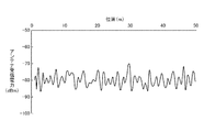
図4は、本発明に係るLCXにおいて測定されたアンテナ受信電力を示すグラフである。 FIG. 4 is a graph showing antenna received power measured in the LCX according to the present invention.
半波長標準ダイポールアンテナ111をLCX1の始端(位置0mの入射端)から、終端(位置50m)まで移動させ、連続して結合損失を測定した。Pinを0dB(1mW)とした。図4に示すように、横軸をLCX1の位置とし、縦軸をアンテナの出力電力Poutとして示すと、出力電力Poutは、多少の変動はあるものの、平均的には−80dBmとなっていた。したがって、結合損失Lcは、設計値通りの80dBが得られたことが確認された。
The half-wavelength standard dipole antenna 111 was moved from the start end (incident end at position 0 m) of LCX1 to the end end (
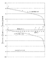
図5は、本発明に係るLCXの結合損失を示すグラフである。 FIG. 5 is a graph showing the coupling loss of the LCX according to the present invention.
図5に示すように、LCX1の位置を横軸とし、縦軸に各位置毎の結合損失、減衰量、0dBmをLCX1に入射した場合のケーブル内電力、及び、LCX1から1.5m離れた位置でのアンテナ出力をとって、LCX1の特性を確認した。 As shown in FIG. 5, the position of LCX1 is on the horizontal axis, and the vertical axis indicates the coupling loss and attenuation at each position, the power in the cable when 0 dBm is incident on LCX1, and the position 1.5 m away from LCX1. The characteristics of LCX1 were confirmed by taking the antenna output at.
位置0m(*1)は、LCX1ヘの信号電力の入射点である。結合損失80dBを設計値としているので、この位置でのLCXの結合損失は80dB(*2)である。LCX1の位置が進むにつれて、ケーブルの減衰量(*3)によってケーブル内電力(*4)は減少していることがわかる。この減少分を補償するために、ケーブルの結合損失(*5)を低下させている。そして、結合損失が50dBを越えると減衰量は急激に増大(*6)するので、LCX1の使用限界は、この位置の50m程度(*7)までであることがわかる。 The position 0m (* 1) is an incident point of signal power to LCX1. Since the coupling loss is 80 dB as a design value, the coupling loss of LCX at this position is 80 dB (* 2). It can be seen that the power in the cable (* 4) decreases with the amount of attenuation (* 3) of the cable as the position of LCX1 advances. In order to compensate for this decrease, the coupling loss (* 5) of the cable is reduced. When the coupling loss exceeds 50 dB, the attenuation increases abruptly (* 6). Therefore, it can be seen that the use limit of LCX1 is up to about 50 m (* 7) at this position.
したがって、ケーブル長は、ケーブルの減衰量が急激に増加する手前まで、すなわち、ケーブル長さ方向について給電側から離れるにしたがって連続的に増加する漏洩電磁界の漏洩量が急激に増加する距離に相当する長さ以下となっていることが好ましい。 Therefore, the cable length is equivalent to the distance at which the leakage amount of the leakage electromagnetic field that continuously increases as the distance from the power supply side increases in the cable length direction, before the cable attenuation increases rapidly. It is preferable that it is below the length to be.
本発明は、漏洩同軸ケーブル及び漏洩同軸ケーブルの製造方法に適用され、特に、スロット部の加工が容易化され、また、結合損失が安定化された漏洩同軸ケーブル及び漏洩同軸ケーブルの製造方法に適用される。 INDUSTRIAL APPLICABILITY The present invention is applied to a leaky coaxial cable and a method of manufacturing a leaky coaxial cable, and in particular, to a leaky coaxial cable and a method of manufacturing a leaky coaxial cable in which processing of a slot portion is facilitated and coupling loss is stabilized. Is done.
1 LCX
101 スロット部
102 中心導体
103 絶縁体
104 外部導体
105 外被(シース)
1 LCX
101 Slot 102 Central conductor 103 Insulator 104 Outer conductor 105 Outer sheath (sheath)
Claims (6)
前記外部導体は、前記スロット部となる開孔の形状がレジストインクにより印刷されて固着された後、金属を腐食させる液中に通過されることにより開孔が形成された金属テープが、前記絶縁体の外周面に巻付けられて構成されたものである
ことを特徴とする漏洩同軸ケーブル。 A center conductor, an insulator covering the center conductor, and an outer conductor covering the outside of the insulator are coaxially structured, and a plurality of slot portions for forming a leakage electromagnetic field are formed in the outer conductor, and the outer conductor A leaky coaxial cable whose conductor is covered with a jacket,
The outer conductor has a hole formed as a slot when the shape of the opening serving as the slot is printed and fixed with a resist ink and then passed through a liquid that corrodes the metal. A leaky coaxial cable characterized by being wound around an outer peripheral surface of a body.
ことを特徴とする請求項1記載の漏洩同軸ケーブル。 The leakage coaxial cable according to claim 1, wherein the leakage amount of the leakage electromagnetic field from the slot portion continuously changes over the entire length of the cable.
ことを特徴とする請求項1、または、請求項2記載の漏洩同軸ケーブル。 The shape of the slot portion continuously changes in the cable length direction, and the leakage amount of the leakage electromagnetic field continuously increases as the distance from the power feeding side increases in the cable length direction, and leakage in the cable length direction. The leaky coaxial cable according to claim 1, wherein a change in the magnitude of the electromagnetic field is suppressed.
ことを特徴とする請求項3記載の漏洩同軸ケーブル。 The cable length is equal to or shorter than a distance corresponding to a distance in which the leakage amount of a leakage electromagnetic field that continuously increases as the distance from the power feeding side increases in the cable length direction. The leaky coaxial cable described.
ことを特徴とする請求項1記載の漏洩同軸ケーブル。 The leaky coaxial cable according to claim 1, wherein the attenuation amount of the cable is selectively changed at a desired location.
金属テープに、漏洩電磁界形成用の複数のスロット部となる開孔の形状をレジストインクにより印刷して固着させる工程と、
前記金属テープを、金属を腐食させる液中に通過させ、該金属テープに開孔を形成する工程と、
前記金属テープを前記絶縁体の外周面に巻付けて、外部導体とする工程と、
前記外部導体を外被で覆う工程と、
を有することを特徴とする漏洩同軸ケーブルの製造方法。 Coating the central conductor with an insulator;
A process of printing and fixing the shape of the opening to be a plurality of slot portions for forming a leakage electromagnetic field on a metal tape with a resist ink;
Passing the metal tape through a solution that corrodes the metal to form openings in the metal tape;
Winding the metal tape around the outer peripheral surface of the insulator to form an outer conductor;
Covering the outer conductor with a jacket;
The manufacturing method of the leaky coaxial cable characterized by having.
Priority Applications (1)
| Application Number | Priority Date | Filing Date | Title |
|---|---|---|---|
| JP2011052725A JP2012191402A (en) | 2011-03-10 | 2011-03-10 | Leaky coaxial cable and method of manufacturing the same |
Applications Claiming Priority (1)
| Application Number | Priority Date | Filing Date | Title |
|---|---|---|---|
| JP2011052725A JP2012191402A (en) | 2011-03-10 | 2011-03-10 | Leaky coaxial cable and method of manufacturing the same |
Publications (1)
| Publication Number | Publication Date |
|---|---|
| JP2012191402A true JP2012191402A (en) | 2012-10-04 |
Family
ID=47084094
Family Applications (1)
| Application Number | Title | Priority Date | Filing Date |
|---|---|---|---|
| JP2011052725A Pending JP2012191402A (en) | 2011-03-10 | 2011-03-10 | Leaky coaxial cable and method of manufacturing the same |
Country Status (1)
| Country | Link |
|---|---|
| JP (1) | JP2012191402A (en) |
Cited By (7)
| Publication number | Priority date | Publication date | Assignee | Title |
|---|---|---|---|---|
| CN104577282A (en) * | 2015-01-09 | 2015-04-29 | 江苏佳汇光电科技有限公司 | Grid type leaky coaxial cable with parallel outer wires and manufacturing method of grid type leaky coaxial cable |
| JP2017188802A (en) * | 2016-04-06 | 2017-10-12 | 日立金属株式会社 | Leaky coaxial cable |
| CN109599678A (en) * | 2017-09-30 | 2019-04-09 | 中天射频电缆有限公司 | A kind of 5G communication waveguide leakage cable |
| CN111029698A (en) * | 2019-12-12 | 2020-04-17 | 安徽联嘉祥特种电缆有限公司 | Coaxial leaky cable for 5G signal transmission |
| WO2022019190A1 (en) * | 2020-07-20 | 2022-01-27 | 株式会社フジクラ・ダイヤケーブル | Leaky coaxial cable |
| CN114094294A (en) * | 2021-11-19 | 2022-02-25 | 中国电信股份有限公司 | Leakage cable |
| CN114798900A (en) * | 2021-10-09 | 2022-07-29 | 长飞光纤光缆股份有限公司 | Device and method for punching outer conductor strip of palindromic structure sectional coupling leaky cable |
Citations (7)
| Publication number | Priority date | Publication date | Assignee | Title |
|---|---|---|---|---|
| JPS5121639Y1 (en) * | 1970-09-12 | 1976-06-04 | ||
| JPH0286303A (en) * | 1988-09-22 | 1990-03-27 | Hitachi Chem Co Ltd | Slot array antenna |
| JPH0365805A (en) * | 1989-08-03 | 1991-03-20 | Sumitomo Bakelite Co Ltd | Waveguide antenna |
| JPH04113708A (en) * | 1990-09-04 | 1992-04-15 | Ocean Cable Co Ltd | Density gradient multi-slot coaxial cable |
| JPH07131236A (en) * | 1993-10-29 | 1995-05-19 | Fujikura Ltd | Leaky coaxial cable |
| JP2005244759A (en) * | 2004-02-27 | 2005-09-08 | Mitsubishi Cable Ind Ltd | Leakage coaxial cable and its manufacturing method |
| JP2010239512A (en) * | 2009-03-31 | 2010-10-21 | Fujikura Ltd | Leakage cable manufacturing method |
-
2011
- 2011-03-10 JP JP2011052725A patent/JP2012191402A/en active Pending
Patent Citations (7)
| Publication number | Priority date | Publication date | Assignee | Title |
|---|---|---|---|---|
| JPS5121639Y1 (en) * | 1970-09-12 | 1976-06-04 | ||
| JPH0286303A (en) * | 1988-09-22 | 1990-03-27 | Hitachi Chem Co Ltd | Slot array antenna |
| JPH0365805A (en) * | 1989-08-03 | 1991-03-20 | Sumitomo Bakelite Co Ltd | Waveguide antenna |
| JPH04113708A (en) * | 1990-09-04 | 1992-04-15 | Ocean Cable Co Ltd | Density gradient multi-slot coaxial cable |
| JPH07131236A (en) * | 1993-10-29 | 1995-05-19 | Fujikura Ltd | Leaky coaxial cable |
| JP2005244759A (en) * | 2004-02-27 | 2005-09-08 | Mitsubishi Cable Ind Ltd | Leakage coaxial cable and its manufacturing method |
| JP2010239512A (en) * | 2009-03-31 | 2010-10-21 | Fujikura Ltd | Leakage cable manufacturing method |
Cited By (12)
| Publication number | Priority date | Publication date | Assignee | Title |
|---|---|---|---|---|
| CN104577282A (en) * | 2015-01-09 | 2015-04-29 | 江苏佳汇光电科技有限公司 | Grid type leaky coaxial cable with parallel outer wires and manufacturing method of grid type leaky coaxial cable |
| JP2017188802A (en) * | 2016-04-06 | 2017-10-12 | 日立金属株式会社 | Leaky coaxial cable |
| CN109599678A (en) * | 2017-09-30 | 2019-04-09 | 中天射频电缆有限公司 | A kind of 5G communication waveguide leakage cable |
| CN109599678B (en) * | 2017-09-30 | 2024-01-12 | 中天射频电缆有限公司 | Waveguide leaky cable for 5G communication |
| CN111029698A (en) * | 2019-12-12 | 2020-04-17 | 安徽联嘉祥特种电缆有限公司 | Coaxial leaky cable for 5G signal transmission |
| WO2022019190A1 (en) * | 2020-07-20 | 2022-01-27 | 株式会社フジクラ・ダイヤケーブル | Leaky coaxial cable |
| CN114798900A (en) * | 2021-10-09 | 2022-07-29 | 长飞光纤光缆股份有限公司 | Device and method for punching outer conductor strip of palindromic structure sectional coupling leaky cable |
| CN114798901A (en) * | 2021-10-09 | 2022-07-29 | 长飞光纤光缆股份有限公司 | Device and method for punching strip of outer conductor of segmented coupling leaky cable |
| CN114798900B (en) * | 2021-10-09 | 2023-01-13 | 长飞光纤光缆股份有限公司 | Device and method for punching outer conductor strip of palindromic structure sectional coupling leaky cable |
| CN114798901B (en) * | 2021-10-09 | 2023-06-23 | 长飞光纤光缆股份有限公司 | A device and method for punching holes in the outer conductor of a segmented coupling leakage cable |
| CN114094294A (en) * | 2021-11-19 | 2022-02-25 | 中国电信股份有限公司 | Leakage cable |
| CN114094294B (en) * | 2021-11-19 | 2023-12-08 | 中国电信股份有限公司 | Leaky cable |
Similar Documents
| Publication | Publication Date | Title |
|---|---|---|
| JP2012191402A (en) | Leaky coaxial cable and method of manufacturing the same | |
| EP2917963B1 (en) | Dual polarization current loop radiator with integrated balun | |
| US8665142B2 (en) | Antenna device and radar device | |
| CN102064372B (en) | Circular leaky waveguide cable | |
| Honari et al. | Investigation of the 3D printing roughness effect on the performance of a dielectric rod antenna | |
| JPWO2007055028A1 (en) | Linearly polarized antenna and radar apparatus using the same | |
| CN104937777A (en) | Antenna | |
| KR100790138B1 (en) | Wideband Logic Cycle Dipole Array Antenna | |
| JP2020088863A (en) | Method of producing waveguide-to-coaxial adapter array, method of producing antenna array, and method of producing waveguiding device | |
| US12482952B2 (en) | Rotated ridge waveguide antenna | |
| JP2019024170A (en) | Dielectric lens antenna device | |
| JP2020065251A (en) | Connection structure between waveguide and coaxial cable | |
| WO2011142231A1 (en) | Cobra antenna | |
| JP5695551B2 (en) | Leaky coaxial cable | |
| JP2018157565A (en) | Leaky coaxial cable and wireless communication system | |
| EP3641052B1 (en) | Antenna device and wireless communication system | |
| JP5631374B2 (en) | antenna | |
| Marrocco et al. | Dielectric resonant antennas via additive manufacturing for 5G communications | |
| Addamo et al. | A Ku-K dual-band compact circular corrugated horn for satellite communications | |
| EP1860725B1 (en) | Radiation-emitting cable and a radiation-emitting element comprised therein | |
| Hirokawa et al. | 94GHz fabrication of a slotted waveguide array antenna by diffusion bonding of laminated thin plates | |
| JP4829840B2 (en) | Antenna device | |
| JP5628879B2 (en) | antenna | |
| KR102772533B1 (en) | Communication line and communication system | |
| JP2015053661A (en) | Antenna device and reflector arrangement method |
Legal Events
| Date | Code | Title | Description |
|---|---|---|---|
| A621 | Written request for application examination |
Free format text: JAPANESE INTERMEDIATE CODE: A621 Effective date: 20131213 |
|
| A977 | Report on retrieval |
Free format text: JAPANESE INTERMEDIATE CODE: A971007 Effective date: 20140612 |
|
| A131 | Notification of reasons for refusal |
Free format text: JAPANESE INTERMEDIATE CODE: A131 Effective date: 20140819 |
|
| A02 | Decision of refusal |
Free format text: JAPANESE INTERMEDIATE CODE: A02 Effective date: 20150511 |