JP2012192538A - Film member, film molded product, method for manufacturing film member, and method for manufacturing film molded product - Google Patents
Film member, film molded product, method for manufacturing film member, and method for manufacturing film molded product Download PDFInfo
- Publication number
- JP2012192538A JP2012192538A JP2011056256A JP2011056256A JP2012192538A JP 2012192538 A JP2012192538 A JP 2012192538A JP 2011056256 A JP2011056256 A JP 2011056256A JP 2011056256 A JP2011056256 A JP 2011056256A JP 2012192538 A JP2012192538 A JP 2012192538A
- Authority
- JP
- Japan
- Prior art keywords
- layer
- film
- metal wiring
- film member
- molded product
- Prior art date
- Legal status (The legal status is an assumption and is not a legal conclusion. Google has not performed a legal analysis and makes no representation as to the accuracy of the status listed.)
- Withdrawn
Links
Images


Classifications
-
- B—PERFORMING OPERATIONS; TRANSPORTING
- B32—LAYERED PRODUCTS
- B32B—LAYERED PRODUCTS, i.e. PRODUCTS BUILT-UP OF STRATA OF FLAT OR NON-FLAT, e.g. CELLULAR OR HONEYCOMB, FORM
- B32B15/00—Layered products comprising a layer of metal
- B32B15/02—Layer formed of wires, e.g. mesh
-
- B—PERFORMING OPERATIONS; TRANSPORTING
- B29—WORKING OF PLASTICS; WORKING OF SUBSTANCES IN A PLASTIC STATE IN GENERAL
- B29C—SHAPING OR JOINING OF PLASTICS; SHAPING OF MATERIAL IN A PLASTIC STATE, NOT OTHERWISE PROVIDED FOR; AFTER-TREATMENT OF THE SHAPED PRODUCTS, e.g. REPAIRING
- B29C45/00—Injection moulding, i.e. forcing the required volume of moulding material through a nozzle into a closed mould; Apparatus therefor
- B29C45/14—Injection moulding, i.e. forcing the required volume of moulding material through a nozzle into a closed mould; Apparatus therefor incorporating preformed parts or layers, e.g. injection moulding around inserts or for coating articles
-
- B—PERFORMING OPERATIONS; TRANSPORTING
- B29—WORKING OF PLASTICS; WORKING OF SUBSTANCES IN A PLASTIC STATE IN GENERAL
- B29C—SHAPING OR JOINING OF PLASTICS; SHAPING OF MATERIAL IN A PLASTIC STATE, NOT OTHERWISE PROVIDED FOR; AFTER-TREATMENT OF THE SHAPED PRODUCTS, e.g. REPAIRING
- B29C45/00—Injection moulding, i.e. forcing the required volume of moulding material through a nozzle into a closed mould; Apparatus therefor
- B29C45/14—Injection moulding, i.e. forcing the required volume of moulding material through a nozzle into a closed mould; Apparatus therefor incorporating preformed parts or layers, e.g. injection moulding around inserts or for coating articles
- B29C45/14778—Injection moulding, i.e. forcing the required volume of moulding material through a nozzle into a closed mould; Apparatus therefor incorporating preformed parts or layers, e.g. injection moulding around inserts or for coating articles the article consisting of a material with particular properties, e.g. porous, brittle
- B29C45/14811—Multilayered articles
-
- B—PERFORMING OPERATIONS; TRANSPORTING
- B32—LAYERED PRODUCTS
- B32B—LAYERED PRODUCTS, i.e. PRODUCTS BUILT-UP OF STRATA OF FLAT OR NON-FLAT, e.g. CELLULAR OR HONEYCOMB, FORM
- B32B15/00—Layered products comprising a layer of metal
- B32B15/04—Layered products comprising a layer of metal comprising metal as the main or only constituent of a layer, which is next to another layer of the same or of a different material
- B32B15/08—Layered products comprising a layer of metal comprising metal as the main or only constituent of a layer, which is next to another layer of the same or of a different material of synthetic resin
-
- B—PERFORMING OPERATIONS; TRANSPORTING
- B32—LAYERED PRODUCTS
- B32B—LAYERED PRODUCTS, i.e. PRODUCTS BUILT-UP OF STRATA OF FLAT OR NON-FLAT, e.g. CELLULAR OR HONEYCOMB, FORM
- B32B27/00—Layered products comprising a layer of synthetic resin
- B32B27/06—Layered products comprising a layer of synthetic resin as the main or only constituent of a layer, which is next to another layer of the same or of a different material
-
- B—PERFORMING OPERATIONS; TRANSPORTING
- B32—LAYERED PRODUCTS
- B32B—LAYERED PRODUCTS, i.e. PRODUCTS BUILT-UP OF STRATA OF FLAT OR NON-FLAT, e.g. CELLULAR OR HONEYCOMB, FORM
- B32B27/00—Layered products comprising a layer of synthetic resin
- B32B27/32—Layered products comprising a layer of synthetic resin comprising polyolefins
-
- B—PERFORMING OPERATIONS; TRANSPORTING
- B29—WORKING OF PLASTICS; WORKING OF SUBSTANCES IN A PLASTIC STATE IN GENERAL
- B29C—SHAPING OR JOINING OF PLASTICS; SHAPING OF MATERIAL IN A PLASTIC STATE, NOT OTHERWISE PROVIDED FOR; AFTER-TREATMENT OF THE SHAPED PRODUCTS, e.g. REPAIRING
- B29C45/00—Injection moulding, i.e. forcing the required volume of moulding material through a nozzle into a closed mould; Apparatus therefor
- B29C45/14—Injection moulding, i.e. forcing the required volume of moulding material through a nozzle into a closed mould; Apparatus therefor incorporating preformed parts or layers, e.g. injection moulding around inserts or for coating articles
- B29C45/1418—Injection moulding, i.e. forcing the required volume of moulding material through a nozzle into a closed mould; Apparatus therefor incorporating preformed parts or layers, e.g. injection moulding around inserts or for coating articles the inserts being deformed or preformed, e.g. by the injection pressure
-
- B—PERFORMING OPERATIONS; TRANSPORTING
- B32—LAYERED PRODUCTS
- B32B—LAYERED PRODUCTS, i.e. PRODUCTS BUILT-UP OF STRATA OF FLAT OR NON-FLAT, e.g. CELLULAR OR HONEYCOMB, FORM
- B32B2605/00—Vehicles
- B32B2605/003—Interior finishings
-
- Y—GENERAL TAGGING OF NEW TECHNOLOGICAL DEVELOPMENTS; GENERAL TAGGING OF CROSS-SECTIONAL TECHNOLOGIES SPANNING OVER SEVERAL SECTIONS OF THE IPC; TECHNICAL SUBJECTS COVERED BY FORMER USPC CROSS-REFERENCE ART COLLECTIONS [XRACs] AND DIGESTS
- Y10—TECHNICAL SUBJECTS COVERED BY FORMER USPC
- Y10T—TECHNICAL SUBJECTS COVERED BY FORMER US CLASSIFICATION
- Y10T428/00—Stock material or miscellaneous articles
- Y10T428/24—Structurally defined web or sheet [e.g., overall dimension, etc.]
- Y10T428/24273—Structurally defined web or sheet [e.g., overall dimension, etc.] including aperture
- Y10T428/24322—Composite web or sheet
- Y10T428/24331—Composite web or sheet including nonapertured component
-
- Y—GENERAL TAGGING OF NEW TECHNOLOGICAL DEVELOPMENTS; GENERAL TAGGING OF CROSS-SECTIONAL TECHNOLOGIES SPANNING OVER SEVERAL SECTIONS OF THE IPC; TECHNICAL SUBJECTS COVERED BY FORMER USPC CROSS-REFERENCE ART COLLECTIONS [XRACs] AND DIGESTS
- Y10—TECHNICAL SUBJECTS COVERED BY FORMER USPC
- Y10T—TECHNICAL SUBJECTS COVERED BY FORMER US CLASSIFICATION
- Y10T428/00—Stock material or miscellaneous articles
- Y10T428/24—Structurally defined web or sheet [e.g., overall dimension, etc.]
- Y10T428/24802—Discontinuous or differential coating, impregnation or bond [e.g., artwork, printing, retouched photograph, etc.]
- Y10T428/24917—Discontinuous or differential coating, impregnation or bond [e.g., artwork, printing, retouched photograph, etc.] including metal layer
Landscapes
- Engineering & Computer Science (AREA)
- Manufacturing & Machinery (AREA)
- Mechanical Engineering (AREA)
- Laminated Bodies (AREA)
- Injection Moulding Of Plastics Or The Like (AREA)
- Structure Of Printed Boards (AREA)
- Shielding Devices Or Components To Electric Or Magnetic Fields (AREA)
Abstract
Description
本発明は、フィルム部材、フィルム成形物、フィルム部材の製造方法、フィルム成形物の製造方法に関する。 The present invention relates to a film member, a film molded product, a method for producing a film member, and a method for producing a film molded product.
従来、例えば、保護層と、着色材が含有された接着層と、基盤層と、を備えた加飾フィルムが知られている。また、この加飾フィルムをフィルムインモールド成形により成形されたプラスチック成形体が知られている(特許文献1参照)。 Conventionally, for example, a decorative film including a protective layer, an adhesive layer containing a colorant, and a base layer is known. Moreover, the plastic molding which shape | molded this decorating film by film-in-mold shaping | molding is known (refer patent document 1).
上記のプラスチック成形体は、例えば、自動車の各種スイッチ類をまとめた操作盤(コンソール)や電子機器の外装等に用いられる。ところで、高度な電子化の発達により、上記の操作盤や外装の内部は、電気配線が密に張り巡らされており、設計の自由度が低下してしまう、という課題があった。 The plastic molded body is used, for example, for an operation panel (console) that collects various switches of an automobile, an exterior of an electronic device, or the like. By the way, due to the development of advanced computerization, there is a problem that the electric wiring is densely arranged inside the operation panel and the exterior, and the degree of freedom in design is reduced.
本発明は、上述の課題の少なくとも一部を解決するためになされたものであり、以下の形態または適用例として実現することが可能である。 SUMMARY An advantage of some aspects of the invention is to solve at least a part of the problems described above, and the invention can be implemented as the following forms or application examples.
[適用例1]本適用例にかかるフィルム部材は、フィルム層と、所定の画像が形成された加飾層と、金属配線が形成された金属配線層と、形状保持層と、を含むことを特徴とする。 [Application Example 1] A film member according to this application example includes a film layer, a decorative layer on which a predetermined image is formed, a metal wiring layer on which metal wiring is formed, and a shape maintaining layer. Features.
この構成によれば、加飾層と金属配線層を備え、加飾層によって視覚的に美観を与えるとともに、他方で金属配線層では電気的接続が可能となる。そして、例えば、当該フィルム部材を成形することにより、これまで困難であった三次元の配線形成を容易に実現することが可能となる。この場合、特に、電気的接続が可能となると、例えば、自動車の操作盤に用いた場合には、内部の電気配線を省くことができ、設計の自由度を高めることができる。 According to this configuration, the decorative layer and the metal wiring layer are provided, and the decorative layer provides visual beauty, while the metal wiring layer enables electrical connection. For example, by forming the film member, it is possible to easily realize three-dimensional wiring formation that has been difficult until now. In this case, in particular, when electrical connection is possible, for example, when used for an operation panel of an automobile, internal electrical wiring can be omitted, and the degree of design freedom can be increased.
[適用例2]上記適用例にかかるフィルム部材は、前記フィルム層と、前記フィルム層上に形成された前記加飾層と、前記加飾層上に形成された接着層と、前記接着層上に配置された前記形状保持層と、前記形状保持層上に形成された前記金属配線層と、を備えたことを特徴とする。 Application Example 2 The film member according to the application example includes the film layer, the decorative layer formed on the film layer, the adhesive layer formed on the decorative layer, and the adhesive layer. And the metal wiring layer formed on the shape-retaining layer.
この構成によれば、加飾層と金属配線層とを三次元成形品として実施することができる。 According to this structure, a decoration layer and a metal wiring layer can be implemented as a three-dimensional molded product.
[適用例3]上記適用例にかかるフィルム部材は、前記フィルム層と、前記フィルム層上に形成された前記加飾層と、前記加飾層上に形成された第1接着層と、前記第1接着層上に形成された遮光層と、前記遮光層上に形成された第2接着層と、前記第2接着層上に形成された前記金属配線層と、前記金属配線層上に形成された前記形状保持層と、を備えたことを特徴とする。 Application Example 3 The film member according to the application example includes the film layer, the decorative layer formed on the film layer, the first adhesive layer formed on the decorative layer, and the first A light shielding layer formed on one adhesive layer; a second adhesive layer formed on the light shielding layer; the metal wiring layer formed on the second adhesive layer; and formed on the metal wiring layer. And the shape retaining layer.
この構成によれば、加飾層と金属配線層とを三次元成形品として実施することができる。 According to this structure, a decoration layer and a metal wiring layer can be implemented as a three-dimensional molded product.
[適用例4]上記適用例にかかるフィルム部材の前記金属配線層は、カーボンナノチューブで形成されたことを特徴とする。 Application Example 4 The metal wiring layer of the film member according to the application example is formed of carbon nanotubes.
この構成によれば、高電気伝導性を有するフィルム部材を提供することができる。 According to this structure, the film member which has high electrical conductivity can be provided.
[適用例5]上記適用例にかかるフィルム部材では、前記金属配線層における前記金属配線が網の目形状を有することを特徴とする。 Application Example 5 In the film member according to the application example, the metal wiring in the metal wiring layer has a mesh shape.
この構成によれば、フィルム部材を延ばした場合に、金属配線に対する応力が緩和されるので、配線の切断を防止することができる。 According to this configuration, when the film member is extended, the stress on the metal wiring is relieved, so that the cutting of the wiring can be prevented.
[適用例6]本適用例にかかるフィルム成形物は、上記のフィルム部材をフィルムインモールドで成形して、モールド樹脂層を備えたことを特徴とする。 Application Example 6 A film molded product according to this application example is characterized in that the film member is formed by film-in-molding and includes a mold resin layer.
この構成によれば、加飾層と金属配線層を備えた三次元成形物を提供することができる。これにより、例えば、自動車の操作盤に用いた場合には、内部の電気配線を省くことができ、設計の自由度を高めることができる。 According to this structure, the three-dimensional molded object provided with the decoration layer and the metal wiring layer can be provided. Thereby, for example, when used for an operation panel of an automobile, internal electrical wiring can be omitted, and the degree of design freedom can be increased.
[適用例7]上記適用例にかかるフィルム成形物は、前記モールド樹脂層の表面から前記金属配線層の表面まで通じる端子案内孔を備えたことを特徴とする。 Application Example 7 A film molded product according to the application example described above is characterized in that a terminal guide hole that leads from the surface of the mold resin layer to the surface of the metal wiring layer is provided.
この構成によれば、モールド樹脂層の表面から金属配線層の表面まで通じる端子案内孔を通じて、容易に電気的接続を行うことができる。 According to this configuration, electrical connection can be easily performed through the terminal guide hole that leads from the surface of the mold resin layer to the surface of the metal wiring layer.
[適用例8]上記適用例にかかるフィルム成形物は、前記フィルム層の表面から前記金属配線層の表面まで通じる端子案内孔を備えたことを特徴とする。 Application Example 8 A film molded product according to the application example described above is characterized in that a terminal guide hole that leads from the surface of the film layer to the surface of the metal wiring layer is provided.
この構成によれば、フィルム層の表面から金属配線層の表面まで通じる端子案内孔を通じて、容易に電気的接続を行うことができる。 According to this configuration, electrical connection can be easily performed through the terminal guide hole that leads from the surface of the film layer to the surface of the metal wiring layer.
[適用例9]本適用例にかかるフィルム部材の製造方法は、フィルム層上に所定の画像を形成する加飾層形成工程と、
金属配線を形成する金属配線層形成工程と、を含むことを特徴とする。
[Application Example 9] A film member manufacturing method according to this application example includes a decorative layer forming step of forming a predetermined image on a film layer;
A metal wiring layer forming step of forming a metal wiring.
この構成によれば、加飾層と金属配線層を備え、加飾層によって視覚的に美観を与えるとともに、他方で金属配線層では電気的接続が可能となる。そして、例えば、当該フィルム部材を成形することにより、これまで困難であった三次元の配線形成を容易に実現することが可能となる。この場合、特に、電気的接続が可能となると、例えば、自動車の操作盤に用いた場合には、内部の電気配線を省くことができ、設計の自由度を高めることができる。 According to this configuration, the decorative layer and the metal wiring layer are provided, and the decorative layer provides visual beauty, while the metal wiring layer enables electrical connection. For example, by forming the film member, it is possible to easily realize three-dimensional wiring formation that has been difficult until now. In this case, in particular, when electrical connection is possible, for example, when used for an operation panel of an automobile, internal electrical wiring can be omitted, and the degree of design freedom can be increased.
[適用例10]本適用例にかかるフィルム成形物の製造方法は、上記のフィルム部材の製造方法によって製造されたフィルム部材を用いてフィルムインモールドを行い、モールド樹脂層を形成するモールド樹脂層形成工程を含むことを特徴とする。 [Application Example 10] A method for producing a film molded product according to this application example includes forming a mold resin layer by performing film-in-molding using the film member produced by the method for producing a film member described above. Including a process.
この構成によれば、加飾層と金属配線層を備えた三次元成形物を提供することができる。これにより、例えば、自動車の操作盤に用いた場合には、内部の電気配線を省くことができ、設計の自由度を高めることができる。 According to this structure, the three-dimensional molded object provided with the decoration layer and the metal wiring layer can be provided. Thereby, for example, when used for an operation panel of an automobile, internal electrical wiring can be omitted, and the degree of design freedom can be increased.
以下、本発明の実施形態について、図面を参照して説明する。なお、以下の各図においては、各層や各部材を認識可能な程度の大きさにするため、各層や各部材の尺度を実際とは異ならせしめている。 Hereinafter, embodiments of the present invention will be described with reference to the drawings. In the following drawings, the scale of each layer and each member is made different from the actual scale so that each layer and each member can be recognized.
[第1実施形態]
(フィルム部材の構成)
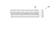
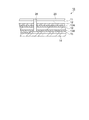
まず、第1実施形態にかかるフィルム部材の構成について説明する。図1は、第1実施形態にかかるフィルム部材の構成を示す断面図である。図1に示すように、フィルム部材1Aは、フィルム層11と、所定の画像が形成された加飾層12と、金属配線が形成された金属配線層15と、形状保持層としてのバッキングシート14等を備えている。
[First Embodiment]
(Structure of film member)
First, the structure of the film member concerning 1st Embodiment is demonstrated. FIG. 1 is a cross-sectional view illustrating a configuration of a film member according to the first embodiment. As shown in FIG. 1, a
さらに、詳細には、フィルム層11と、フィルム層11上に形成された加飾層12と、加飾層12上に形成された接着層13と、接着層13上に配置されたバッキングシート14と、バッキングシート14上に形成された金属配線層15とを備えている。なお、本実施形態では、フィルム層11の表面には、フィルム層11を保護する保護層20が設けられている。
More specifically, the
フィルム層11は、表面が平滑で透明性を有する熱可塑性樹脂から構成される。上記透明性とは加飾層12が透視可能な程度を意味する。従って、無色透明でもよいし、着色透明であってもよい。フィルム層11は、例えば、10〜500μm程度である。熱可塑性樹脂としては、アクリル樹脂、ポリオレフィン系樹脂、ポリエステル樹脂、ポリカーボネート樹脂、ポリアミド樹脂、ポリスチレン、AS(アクリロニトリル−スチレン共重合体)樹脂、ポリ塩化ビニル、塩化ビニル−酢酸ビニル共重合体等の1種単独或いは2種以上の混合物等が用いられる。なお、本実施形態では、フィルム層11上に保護膜20を備えたが、当該保護膜20を省略してもよい。この場合において、フィルム層11に、炭化水素系滑剤、脂肪酸系滑剤などの滑剤を添加してもよい。このようにすれば、耐擦傷性等を保持することができる。
The
加飾層12は、図柄や絵柄等の画像を形成することにより装飾効果を高めるものである。例えば、木目模様、石目模様、砂目模様、タイル貼調模様、煉瓦積調模様、布目模様、皮絞模様、文字、記号、図形、幾何学模様、単独又は組み合わせで適宜形成される。加飾層12は、例えば、インクジェット法を用いて形成することができる。この場合、紫外線硬化型インクを吐出ヘッドから液滴として、フィルム層11上に紫外線硬化型インクを塗布する。そして、塗布された紫外線硬化型インクに紫外線を照射して、フィルム層11上に紫外線硬化型インクを定着させることにより形成される。なお、インクジェット法で用いられるインクは、紫外線硬化型のものに限られず、赤外線硬化型や可視光硬化型等のインクでもよい。この場合、硬化に適した光源を用いればよい。また水系インクや溶剤系インクでもよい。さらには、インクジェット法に限らず、例えば、グラビア印刷、活版印刷、シルクスクリーン印刷、オフセット印刷、フレキソ印刷等を適宜適用することができる。
The
バッキングシート14は、成形した際に形状を保持するものである。例えば、アクリル樹脂、ポリオレフィン系樹脂、ポリエステル樹脂、ポリカーボネート樹脂、ポリアミド樹脂、ポリスチレン、AS(アクリロニトリル−スチレン共重合体)樹脂、ポリ塩化ビニル、塩化ビニル−酢酸ビニル共重合体等の1種単独或いは2種以上の混合物等が用いられる。また、バッキングシート14は、透明性が要求されない場合には、ABS(アクリロニトリル・ブタジエン・スチレン共重合体)を用いてもよい。
The
金属配線層15は、金属配線が形成された層である。金属配線層15は、例えば、インクジェット法を用いて形成することができる。この場合、導電性微粒子を含む機能液を液滴として吐出し、バッキングシート14上に機能液を塗布する。そして、塗布された機能液を固化させることにより金属配線が形成される。導電性微粒子は、数nm〜数十nmの粒径を有し、例えば銀、金、銅、白金、パラジウム、ロジウム、オスミウム、ルテニウム、イリジウム、鉄、錫、コバルト、ニッケル、クロム、チタン、タンタル、タングステン、インジウム等の金属、あるいはこれらの合金である。ここで言う機能液の固化とは、機能液に含まれる導電性微粒子同士が融着して、金属配線の導電性を示す状態のことである。
The
また、金属配線を、カーボンナノチューブを用いて形成してもよい。カーボンナノチューブは、高い電気伝導性、優れた機械的特性を有するため、高品質なフィルム部材、成形物を提供することができる。 Further, the metal wiring may be formed using carbon nanotubes. Since carbon nanotubes have high electrical conductivity and excellent mechanical properties, high quality film members and molded products can be provided.
なお、金属配線層15の形成は、インクジェット法に限らず、例えば、グラビア印刷、活版印刷、シルクスクリーン印刷、オフセット印刷、フレキソ印刷等を適宜適用することができる。
The formation of the
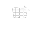
図2は、第1実施形態にかかるフィルム部材の金属配線のパターン例を示す模式図である。図2に示すように、金属配線層15における金属配線15aは、網の目形状(メッシュ形状)を有している。これにより、例えば、成形時においてフィルム部材が延ばされたときに応力が緩和され金属配線15aの断線を防止することができる。なお、例えば、金属配線15aの形成位置や成形部位等を考慮して、金属配線15aの幅、厚み、網の目形状の密度等を適宜設定することができる。
FIG. 2 is a schematic diagram illustrating a pattern example of the metal wiring of the film member according to the first embodiment. As shown in FIG. 2, the
(フィルム部材の製造方法)
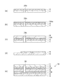
次に、第1実施形態にかかるフィルム部材の製造方法について説明する。図3は、第1実施形態にかかるフィルム部材の製造方法を示す工程図である。図3に示すように、フィルム部材の製造方法は、フィルム層上に所定の画像を形成する加飾層形成工程と、金属配線を形成する金属配線層形成工程と、を含むものである。以下、詳細に説明する。
(Film member manufacturing method)
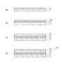
Next, the manufacturing method of the film member concerning 1st Embodiment is demonstrated. Drawing 3 is a flowchart showing the manufacturing method of the film member concerning a 1st embodiment. As shown in FIG. 3, the manufacturing method of a film member includes the decoration layer formation process which forms a predetermined | prescribed image on a film layer, and the metal wiring layer formation process which forms metal wiring. Details will be described below.
まず、図3(a)の加飾層形成工程では、フィルム層11上に加飾層12を形成する。例えば、インクジェット法を用いて、フィルム層11に向けて、機能液を液滴として吐出し、フィルム層11上に機能液を塗布する。そして、塗布された機能液を固化させることにより、加飾層12が形成される。なお、加飾層12の形成方法は、インクジェット法に限定されず、例えば、グラビア印刷、活版印刷、シルクスクリーン印刷、オフセット印刷、フレキソ印刷等を適宜適用することができる。
First, in the decorative layer forming step of FIG. 3A, the
次いで、図3(b)の接着剤塗布工程では、加飾層12上に接着剤13aを塗布する。
Next, in the adhesive application step of FIG. 3B, the adhesive 13 a is applied on the
次いで、図3(c)のバッキングシート配置工程では、接着剤13a上にバッキングシート14を配置し、接着剤13aを固化することにより、接着層13が形成されるとともに、接着層13上にバッキングシート14が配置される。
Next, in the backing sheet arranging step of FIG. 3C, the
次いで、図3(d)の金属配線層形成工程では、バッキングシート14上に金属配線を形成する。例えば、インクジェット法を用いて、フィルム層11に向けて、導電性微粒子を含む機能液を液滴として吐出し、バッキングシート14上に機能液を塗布する。そして、塗布された機能液を固化させることにより、金属配線が形成される。また、カーボンナノチューブを含む機能液を液滴として吐出し、これを固化して金属配線を形成してもよい。さらに、金属配線層形成工程では、図2に示すように、網の目形状に金属配線15aを形成してもよい。なお、加飾層12の形成方法は、インクジェット法に限定されず、例えば、グラビア印刷、活版印刷、シルクスクリーン印刷、オフセット印刷、フレキソ印刷等を適宜適用することができる。
Next, in the metal wiring layer forming step of FIG. 3D, metal wiring is formed on the
以上、上記工程を経ることにより、フィルム部材1Aが形成される(図1参照)。
As described above, the
(フィルム成形物の構成)
次に、第1実施形態にかかるフィルム成形物の構成について説明する。図4は、第1実施形態にかかるフィルム成形物の構成を示す断面図である。図4に示すように、フィルム成形物10Aは、フィルム部材1Aをフィルムインモールドして、モールド樹脂層22を備えたものである。本実施形態では、金属配線層15を覆うようにモールド樹脂層22が形成されている。なお、フィルム部材1Aの構成は、図1と同様なので、説明を省略する。
(Structure of film molding)
Next, the structure of the film molding concerning 1st Embodiment is demonstrated. FIG. 4 is a cross-sectional view showing the configuration of the film molded product according to the first embodiment. As shown in FIG. 4, the film molded product 10 </ b> A is provided with a
モールド樹脂層22は、例えば、ABS(アクリロニトリル・ブタジエン・スチレン共重合体)樹脂、AS(アクリロニトリル・スチレン共重合体)樹脂、ポリスチレン、ポリ塩化ビニル、ポリオレフィン樹脂、アクリル樹脂、ポリカーボネート樹脂等の熱可塑性樹脂を加熱熔融して液状乃至流動状態となったもの、或いは二液硬化型、触媒硬化型の樹脂、例えば、ウレタン樹脂、ポリエステル樹脂等の未硬化液等で構成されている。
The
また、本実施形態のフィルム成形物10Aには、モールド樹脂層22の表面から金属配線層15の表面まで通じる端子案内孔27が設けられている。これにより、外部との電気接続が可能となる。
Further, terminal guide holes 27 that lead from the surface of the
(フィルム成形物の製造方法)
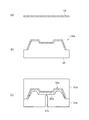
次に、第1実施形態にかかるフィルム成形物の製造方法について説明する。図5は、第1実施形態にかかるフィルム成形物の製造方法を示す工程図である。本実施形態のフィルム成形物の製造方法は、フィルム部材1Aを用いてフィルムインモールドを行ってモールド樹脂層22を形成するモールド樹脂層形成工程を含むものである。以下、詳細に説明する。
(Production method of film molding)
Next, the manufacturing method of the film molding concerning 1st Embodiment is demonstrated. FIG. 5 is a process diagram showing a method for producing a film molded product according to the first embodiment. The manufacturing method of the film molding of this embodiment includes the mold resin layer formation process which forms a
まず、図5(a)に示すように、フィルム部材1Aを用意する。なお、フィルム部材1Aの製造方法は、図3に示す製造方法と同様なので説明を省略する。
First, as shown in FIG. 5A, a
次いで、図5(b)に示すように、フィルム部材1Aを成形する。本実施形態では、真空成形型30を用いて、フィルム部材1Aを真空成形する。具体的には、加熱により軟化したフィルム部材1Aを真空成形型30上に載置し、真空成形型に設けられた吸引孔(図示せず)から空気を吸引する。そうすると、図5(b)に示すように、真空成形型30の表面形状に倣ったフィルム部材1Aaが形成される。
Next, as shown in FIG. 5B, the
次いで、図5(c)に示すように、真空成形されたフィルム部材1Aaを用いて射出成形する。具体的には、真空成形されたフィルム部材1Aaを射出成形型の第1金型31aと第2金型31bとで挟み込み、モールド樹脂注入口31cからモールド樹脂をフィルム部材1Aaに向けて注入する。そうすると、フィルム部材1Aaにモールド樹脂22aが金型内に充填される。そして、モールド樹脂22aを固化させた後、第1金型31aと第2金型31bを開放させ、射出成形型から射出成形品を取出す。なお、本射出成形型の第2金型31bには、立てピン(図示せず)が設けられており、フィルム部材1Aaを第1金型31aと第2金型31bとで挟んだときに、立てピンの頂部がフィルム部材1Aaの金属配線層15に接触するように構成されている。このようにして、端子案内孔27が形成される。
Next, as shown in FIG. 5C, injection molding is performed using the vacuum-formed film member 1Aa. Specifically, the vacuum-formed film member 1Aa is sandwiched between the
以上、上記工程を経ることにより、フィルム成形物10Aが形成される(図4参照)。
As described above, the film molded
従って、第1実施形態によれば、以下に示す効果がある。 Therefore, according to the first embodiment, the following effects can be obtained.
フィルム部材1Aおよびフィルム成形物10Aでは、加飾層12と金属配線層15を具備した。これにより、加飾層12は目視において装飾性を与えるとともに、他方で金属配線層15では電気的接続が可能となり、設計の自由度を高めることができる。例えば、自動車の操作盤に用いた場合には、モールド樹脂層22に設けられ端子案内孔27から電気回路パターンに形成された金属配線層15に接続することにより、電気配線の引き回し本数を省くことができる。
In the
[第2実施形態]
(フィルム部材の構成)
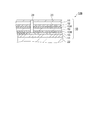
次に、第2実施形態にかかるフィルム部材の構成について説明する。図6は、第2実施形態にかかるフィルム部材の構成を示す断面図である。図6に示すように、フィルム部材1Bは、フィルム層11と、所定の画像が形成された加飾層12と、金属配線が形成された金属配線層15と、形状保持層としてのバッキングシート14等を備えている。
[Second Embodiment]
(Structure of film member)
Next, the structure of the film member concerning 2nd Embodiment is demonstrated. FIG. 6 is a cross-sectional view showing a configuration of a film member according to the second embodiment. As shown in FIG. 6, the
さらに、詳細には、フィルム層11と、フィルム層11上に形成された加飾層12と、加飾層12上に形成された第1接着層13Aと、第1接着層13A上に配置された遮光層19と、遮光層19上に形成された第2接着層13Bと、第2接着層13B上に形成された金属配線層15と、金属配線層15上に形成されたバッキングシート14とを備えている。なお、本実施形態では、フィルム層11の表面には、フィルム層11を保護する保護層20が設けられている。そして、フィルム層11の表面から金属配線層15の表面まで通じる端子案内孔28を備えている。なお、本実施形態では、フィルム層11の表面には、フィルム層11を保護する保護層20が設けられている。このため、端子案内孔28は、保護膜20表面から金属配線層15の表面まで通じて形成されている。
More specifically, the
フィルム層11、加飾層12、金属配線層15、バッキングシート14の形態等については第1実施形態と同様なので説明を省略する。
Since the
遮光層19は、保護膜20側から加飾層12を目視した場合に、金属配線層15等のパターンや着色等が透けて見えることを防止するための層である。遮光層19は、例えば、ABS(アクリロニトリル・ブタジエン・スチレン共重合体)等を適用することができる。
The
図2は、第1実施形態にかかるフィルム部材の金属配線のパターン例を示す模式図である。図2に示すように、金属配線層15における金属配線15aは、網の目形状(メッシュ形状)を有している。これにより、延ばしたときに応力緩和で金属配線15aの断線を防止することができる。なお、例えば、金属配線15aの形成位置や成形部位等を考慮して、金属配線15aの幅、厚み、網の目形状の密度等を適宜設定することができる。
FIG. 2 is a schematic diagram illustrating a pattern example of the metal wiring of the film member according to the first embodiment. As shown in FIG. 2, the
(フィルム部材の製造方法)
次に、第2実施形態にかかるフィルム部材の製造方法について説明する。図7は、第2実施形態にかかるフィルム部材の製造方法を示す工程図である。図7を示すように、フィルム部材の製造方法は、フィルム層上に所定の画像を形成する加飾層形成工程と、金属配線を形成する金属配線層形成工程と、を含むものである。以下、詳細に説明する。
(Film member manufacturing method)
Next, the manufacturing method of the film member concerning 2nd Embodiment is demonstrated. FIG. 7 is a process diagram showing a method for manufacturing a film member according to the second embodiment. As shown in FIG. 7, the method for manufacturing a film member includes a decorative layer forming step for forming a predetermined image on the film layer and a metal wiring layer forming step for forming metal wiring. Details will be described below.
まず、図7(a)の加飾層形成工程では、所定の箇所に貫通孔28aが形成れたフィルム層11上に加飾層12を形成する。例えば、インクジェット法を用いて、フィルム層11に向けて、機能液を液滴として吐出し、フィルム層11上に機能液を塗布する。そして、塗布された機能液を固化させることにより、加飾層12が形成される。なお、加飾層12の形成方法は、インクジェット法に限定されず、例えば、グラビア印刷、活版印刷、シルクスクリーン印刷、オフセット印刷等を適宜適用することができる。
First, in the decorative layer forming step of FIG. 7A, the
次いで、図7(b)の接着剤塗布工程では、加飾層12上に第1接着剤13Aaを塗布する。このとき、貫通孔28bが形成される。
Next, in the adhesive application step of FIG. 7B, the first adhesive 13 </ b> Aa is applied on the
次いで、図7(c)の遮光層形成工程では、第1接着剤13Aa上に遮光層19を形成し、第1接着剤13Aaを固化する。これにより、第1接着層13Aが形成されるとともに、第1接着層13上に遮光層19が形成される。このとき、貫通孔28cが形成される。
Next, in the light shielding layer forming step of FIG. 7C, the
以上の図7(a)〜(c)に示した接着剤塗布工程〜遮光層形成工程とは別に、以下の工程が実施される。 Apart from the adhesive application step to the light shielding layer forming step shown in FIGS. 7 (a) to (c), the following steps are performed.
図7(d)の金属配線層形成工程では、バッキングシート14上に金属配線を形成する。例えば、インクジェット法を用いて、導電性微粒子を含む機能液を液滴として吐出し、バッキングシート14上に機能液を塗布する。そして、塗布された機能液を固化させることにより、金属配線が形成される。また、カーボンナノチューブを含む機能液を液滴として吐出し、これを固化して金属配線を形成してもよい。さらに、金属配線層形成工程では、図2に示すように、網の目形状に金属配線15aを形成してもよい。なお、加飾層12の形成方法は、インクジェット法に限定されず、例えば、グラビア印刷、活版印刷、シルクスクリーン印刷、オフセット印刷、フレキソ印刷等を適宜適用することができる。
In the metal wiring layer forming step of FIG. 7D, metal wiring is formed on the
次いで、図7(e)に示すように、図7(a)〜(c)に示した接着剤塗布工程〜遮光層形成工程で形成された形成物と、図7(d)に示した金属配線層形成工程で形成された形成物とを第2接着剤13Baを介して接着させる。そして、第2接着剤13Baを固化することにより、第2接着層13Bが形成される。
Next, as shown in FIG. 7 (e), the formed product formed in the adhesive application step to the light shielding layer forming step shown in FIGS. 7 (a) to (c) and the metal shown in FIG. 7 (d). The formed product formed in the wiring layer forming step is bonded via the second adhesive 13Ba. Then, the second
以上、上記工程を経ることにより、フィルム部材1Bが形成される(図6参照)。
As described above, the
(フィルム成形物の構成)
次に、第2実施形態にかかるフィルム成形物の構成について説明する。図8は、第2実施形態にかかるフィルム成形物の構成を示す断面図である。図8に示すように、フィルム成形物10Bは、フィルム部材1Bをフィルムインモールドして、モールド樹脂層22を備えたものである。本実施形態では、バッキングシート14を覆うようにモールド樹脂層22が形成されている。なお、フィルム部材1Bの構成は、図6と同様なので、説明を省略する。
(Structure of film molding)
Next, the structure of the film molding concerning 2nd Embodiment is demonstrated. FIG. 8 is a cross-sectional view showing a configuration of a film molded product according to the second embodiment. As shown in FIG. 8, the film molded product 10 </ b> B includes a molded
モールド樹脂層22は、例えば、ABS(アクリロニトリル・ブタジエン・スチレン共重合体)樹脂、AS(アクリロニトリル・スチレン共重合体)樹脂、ポリスチレン、ポリ塩化ビニル、ポリオレフィン樹脂、アクリル樹脂、ポリカーボネート樹脂等の熱可塑性樹脂を加熱熔融して液状乃至流動状態となったもの、或いは二液硬化型、触媒硬化型の樹脂、例えば、ウレタン樹脂、ポリエステル樹脂等の未硬化液等で構成されている。
The
また、本実施形態のフィルム成形物10Bには、保護膜20の表面から金属配線層15の表面まで通じる端子案内孔28が設けられている。これにより、端子案内孔28を通じて外部との電気接続が可能となる。
The film molded product 10 </ b> B of the present embodiment is provided with terminal guide holes 28 that lead from the surface of the
(フィルム成形物の製造方法)
次に、第2実施形態にかかるフィルム成形物の製造方法について説明する。図9は、第2実施形態にかかるフィルム成形物の製造方法を示す工程図である。本実施形態のフィルム成形物の製造方法は、フィルム部材1Bを用いてフィルムインモールドを行ってモールド樹脂層22を形成するモールド樹脂層形成工程を含むものである。以下、詳細に説明する。
(Production method of film molding)
Next, the manufacturing method of the film molding concerning 2nd Embodiment is demonstrated. FIG. 9 is a process diagram showing a method for producing a film molded product according to the second embodiment. The manufacturing method of the film molding of this embodiment includes the mold resin layer formation process which forms a
まず、図9(a)に示すように、フィルム部材1Bを用意する。なお、フィルム部材1Bの製造方法は、図7に示す製造方法と同様なので説明を省略する。
First, as shown in FIG. 9A, a
次いで、図9(b)に示すように、フィルム部材1Bを成形する。本実施形態では、真空成形型30を用いて、フィルム部材1Bを真空成形する。具体的には、加熱により軟化したフィルム部材1Bを真空成形型30上に載置し、真空成形型に設けられた吸引孔(図示せず)から空気を吸引する。そうすると、図9(b)に示すように、真空成形型30の表面形状に倣ったフィルム部材1Baが形成される。
Next, as shown in FIG. 9B, the
次いで、図9(c)に示すように、真空成形されたフィルム部材1Baを用いて射出成形する。具体的には、真空成形されたフィルム部材1Baを射出成形型の第1金型31aと第2金型31bとで挟み込み、モールド樹脂注入口31cからモールド樹脂をフィルム部材1Baに向けて注入する。そうすると、フィルム部材1Baにモールド樹脂22aが金型内に充填される。そして、モールド樹脂22aを固化させた後、第1金型31aと第2金型31bを開放させ、射出成形型から射出成形品を取出す。
Next, as shown in FIG. 9C, injection molding is performed using the vacuum-formed film member 1Ba. Specifically, the vacuum-formed film member 1Ba is sandwiched between an injection mold
以上、上記工程を経ることにより、フィルム成形物10Bが形成される(図8参照)。
As described above, the film molded
従って、第2実施形態によれば、以下に示す効果がある。 Therefore, according to the second embodiment, the following effects can be obtained.
フィルム部材1Bおよびフィルム成形物10Bでは、加飾層12と金属配線層15を具備した。これにより、加飾層12は目視において装飾性を与えるとともに、他方で金属配線層15では電気的接続が可能となり、設計の自由度を高めることができる。例えば、自動車の操作盤に用いた場合には、保護膜20の表面から金属配線層15に通じて形成された端子案内孔28から電気回路パターンに形成された金属配線層15に接続することにより、電気配線の引き回し本数を省くことができる。
In the
なお、本発明は上述した実施形態に限定されず、上述した実施形態に種々の変更や改良などを加えることが可能である。変形例を以下に述べる。 Note that the present invention is not limited to the above-described embodiment, and various modifications and improvements can be added to the above-described embodiment. A modification will be described below.
(変形例1)第1実施形態では、図4に示すように、モールド樹脂層22に端子案内孔27を設けたが、これに限定されない。例えば、保護膜20の表面から金属配線15aに通じる他の端子案内孔を形成してもよい。このようにすれば、外部から電気接続を取り得る箇所が増えるので、さらに、設計の自由度を高めることができる。同様にして、第2実施形態では、図8に示すように、保護膜20の表面から金属配線層15に通じる端子案内孔28を設けたが、これに限定されない。例えば、モールド樹脂層22の表面から金属配線層15に通じる他の端子案内孔を形成してもよい。このようにすれば、外部から電気接続を取り得る箇所が増えるので、さらに、設計の自由度を高めることができる。
(Modification 1) In the first embodiment, the
(変形例2)上記実施形態では、金属配線層15を、電気配線の代替え手段として説明したが、これに限定されない。例えば、アンテナや電磁波シールド等に適宜適用することができる。このようにすれば、上記同様に、部品の点数を削減し、設計の自由度を高めることができる。
(Modification 2) In the above embodiment, the
1A,1B…フィルム部材、1Aa,1Ba…フィルム部材、10A,10B…フィルム成形物、11…フィルム層、12…加飾層、13…接着層、13A…第1接着層、13B…第2接着層、14…形状保持層としてのバッキングシート、15…金属配線層、15a…金属配線、19…遮光層、20…保護膜、22…モールド樹脂層、27,28…端子案内孔、30…真空成形型、31a…第1金型、31b…第2金型。
DESCRIPTION OF
Claims (10)
所定の画像が形成された加飾層と、
金属配線が形成された金属配線層と、
形状保持層と、を含むことを特徴とするフィルム部材。 A film layer;
A decorative layer on which a predetermined image is formed;
A metal wiring layer on which metal wiring is formed; and
A film member comprising a shape-retaining layer.
前記フィルム層と、
前記フィルム層上に形成された前記加飾層と、
前記加飾層上に形成された接着層と、
前記接着層上に配置された前記形状保持層と、
前記形状保持層上に形成された前記金属配線層と、を備えたことを特徴とするフィルム部材。 The film member according to claim 1,
The film layer;
The decorative layer formed on the film layer;
An adhesive layer formed on the decorative layer;
The shape retention layer disposed on the adhesive layer;
And a metal wiring layer formed on the shape retention layer.
前記フィルム層と、
前記フィルム層上に形成された前記加飾層と、
前記加飾層上に形成された第1接着層と、
前記第1接着層上に形成された遮光層と、
前記遮光層上に形成された第2接着層と、
前記第2接着層上に形成された前記金属配線層と、
前記金属配線層上に形成された前記形状保持層と、を備えたことを特徴とするフィルム部材。 The film member according to claim 1,
The film layer;
The decorative layer formed on the film layer;
A first adhesive layer formed on the decorative layer;
A light shielding layer formed on the first adhesive layer;
A second adhesive layer formed on the light shielding layer;
The metal wiring layer formed on the second adhesive layer;
A film member, comprising: the shape retention layer formed on the metal wiring layer.
前記金属配線層は、カーボンナノチューブで形成されたことを特徴とするフィルム部材。 In the film member according to any one of claims 1 to 3,
The film member, wherein the metal wiring layer is formed of carbon nanotubes.
前記金属配線層における前記金属配線が網の目形状を有することを特徴とするフィルム部材。 In the film member as described in any one of Claims 1-4,
The film member, wherein the metal wiring in the metal wiring layer has a mesh shape.
前記モールド樹脂層の表面から前記金属配線層の表面まで通じる端子案内孔を備えたことを特徴とするフィルム成形物。 In the film molded product according to claim 6,
A film molded article comprising terminal guide holes that lead from the surface of the mold resin layer to the surface of the metal wiring layer.
前記フィルム層の表面から前記金属配線層の表面まで通じる端子案内孔を備えたことを特徴とするフィルム成形物。 In the film molded product according to claim 6,
A film molded article comprising terminal guide holes that lead from the surface of the film layer to the surface of the metal wiring layer.
金属配線を形成する金属配線層形成工程と、を含むことを特徴とするフィルム部材の製造方法。 A decorative layer forming step of forming a predetermined image on the film layer;
And a metal wiring layer forming step of forming a metal wiring.
Priority Applications (4)
| Application Number | Priority Date | Filing Date | Title |
|---|---|---|---|
| JP2011056256A JP2012192538A (en) | 2011-03-15 | 2011-03-15 | Film member, film molded product, method for manufacturing film member, and method for manufacturing film molded product |
| US13/410,809 US20120237723A1 (en) | 2011-03-15 | 2012-03-02 | Film member, film molded product, film member producing method, and film molded product producing method |
| KR1020120022188A KR20120105360A (en) | 2011-03-15 | 2012-03-05 | Film member, film molded product, film member producing method and film molded product producing method |
| CN2012100658835A CN102673045A (en) | 2011-03-15 | 2012-03-13 | Film member, film molded product, film member producing method, and film molded product producing method |
Applications Claiming Priority (1)
| Application Number | Priority Date | Filing Date | Title |
|---|---|---|---|
| JP2011056256A JP2012192538A (en) | 2011-03-15 | 2011-03-15 | Film member, film molded product, method for manufacturing film member, and method for manufacturing film molded product |
Publications (1)
| Publication Number | Publication Date |
|---|---|
| JP2012192538A true JP2012192538A (en) | 2012-10-11 |
Family
ID=46805906
Family Applications (1)
| Application Number | Title | Priority Date | Filing Date |
|---|---|---|---|
| JP2011056256A Withdrawn JP2012192538A (en) | 2011-03-15 | 2011-03-15 | Film member, film molded product, method for manufacturing film member, and method for manufacturing film molded product |
Country Status (4)
| Country | Link |
|---|---|
| US (1) | US20120237723A1 (en) |
| JP (1) | JP2012192538A (en) |
| KR (1) | KR20120105360A (en) |
| CN (1) | CN102673045A (en) |
Cited By (2)
| Publication number | Priority date | Publication date | Assignee | Title |
|---|---|---|---|---|
| JP2018502454A (en) * | 2014-12-23 | 2018-01-25 | ティーイー・コネクティビティ・コーポレイションTE Connectivity Corporation | Electronic component and overmolding method |
| JP2020086523A (en) * | 2018-11-15 | 2020-06-04 | 尾池工業株式会社 | Flexible decorative laminated sheet, module for touch panel and touch panel |
Families Citing this family (3)
| Publication number | Priority date | Publication date | Assignee | Title |
|---|---|---|---|---|
| JP6576899B2 (en) * | 2016-10-21 | 2019-09-18 | Nissha株式会社 | Decorative layer / resin laminated structure housing and manufacturing apparatus thereof |
| US20190329464A1 (en) * | 2017-01-31 | 2019-10-31 | Mitsubishi Heavy Industries, Ltd. | Method for determining thickness of resin layer of insert film, method for manufacturing insert film-equipped molded resin article, and insert film |
| DE102019127108A1 (en) * | 2019-10-09 | 2021-04-15 | Leonhard Kurz Stiftung & Co. Kg | Method and device for producing a plastic component and a plastic component |
Family Cites Families (5)
| Publication number | Priority date | Publication date | Assignee | Title |
|---|---|---|---|---|
| JP2005039080A (en) * | 2003-07-16 | 2005-02-10 | Toppan Printing Co Ltd | Conductor wiring laminate substrate and conductor wiring substrate |
| US20070257398A1 (en) * | 2006-05-04 | 2007-11-08 | Moncrieff Scott E | Laminated electronic components for insert molding |
| CN101458601B (en) * | 2007-12-14 | 2012-03-14 | 清华大学 | Touch screen and display device |
| US8238073B2 (en) * | 2008-07-18 | 2012-08-07 | Synaptics, Inc. | In-molded capacitive sensors |
| CN101655628B (en) * | 2009-09-22 | 2011-09-28 | 协晶电子科技(上海)有限公司 | Show-window type touch information display screen based on touch sense film and show system thereof |
-
2011
- 2011-03-15 JP JP2011056256A patent/JP2012192538A/en not_active Withdrawn
-
2012
- 2012-03-02 US US13/410,809 patent/US20120237723A1/en not_active Abandoned
- 2012-03-05 KR KR1020120022188A patent/KR20120105360A/en not_active Withdrawn
- 2012-03-13 CN CN2012100658835A patent/CN102673045A/en active Pending
Cited By (4)
| Publication number | Priority date | Publication date | Assignee | Title |
|---|---|---|---|---|
| JP2018502454A (en) * | 2014-12-23 | 2018-01-25 | ティーイー・コネクティビティ・コーポレイションTE Connectivity Corporation | Electronic component and overmolding method |
| JP2020086523A (en) * | 2018-11-15 | 2020-06-04 | 尾池工業株式会社 | Flexible decorative laminated sheet, module for touch panel and touch panel |
| JP7063464B2 (en) | 2018-11-15 | 2022-05-09 | 尾池工業株式会社 | Flexible decorative laminated sheet, touch panel module and touch panel |
| US11681386B2 (en) | 2018-11-15 | 2023-06-20 | Oike & Co., Ltd. | Flexible decorative laminate sheet, module for touch panel, and touch panel |
Also Published As
| Publication number | Publication date |
|---|---|
| US20120237723A1 (en) | 2012-09-20 |
| KR20120105360A (en) | 2012-09-25 |
| CN102673045A (en) | 2012-09-19 |
Similar Documents
| Publication | Publication Date | Title |
|---|---|---|
| JP5066182B2 (en) | Insert molding laminate and manufacturing method thereof, insert molding product and manufacturing method thereof | |
| US9815241B2 (en) | Method of 3D printing plastic molding compound on foil ply | |
| CN1243632C (en) | Injection-moulded decorative product and its production method | |
| CN103252867B (en) | Mould internal resistance element and shielding element | |
| JP2012192538A (en) | Film member, film molded product, method for manufacturing film member, and method for manufacturing film molded product | |
| US20140120329A1 (en) | Decoration film, decorated molded device and decoration molding process | |
| CN105027045B (en) | Touch panel, method for producing the same, molded product, method for producing the same, and laminated film | |
| JPWO2008035736A1 (en) | Housing case, method for manufacturing the housing case, and glass insert molding die used therefor | |
| CN101765824A (en) | Protection panel with touch input function and method for producing the protection panel | |
| JP6686626B2 (en) | Decorative sheet and decorative resin molded product | |
| KR20040063003A (en) | Key sheet member and its production method | |
| TW200933675A (en) | Method of manufacturing key with three-dimensional pattern | |
| US20120003433A1 (en) | Decoration film, decoration device, and method for manufacturing decoration device | |
| TW201620708A (en) | Molded article, electrical component sheet, and method for manufacturing molded article and electrical product | |
| JP2009119715A (en) | Decorative resin molded product with a cooling sensation layer | |
| EP4297981A1 (en) | Laminate with a decorative layer, composite made up of a laminate and a moulding, and method for producing the laminate | |
| KR102681922B1 (en) | Masking pattern, and manufacturing method of symbol button for automobile by using the same | |
| JP4676607B2 (en) | Injection molding simultaneous painting method | |
| JP2012195334A (en) | Manufacturing method of film molding | |
| CN111190508B (en) | Flexible decorative laminated sheet, assembly for touch panel, and touch panel | |
| JP2017065168A (en) | Manufacturing method of decorative resin molded article | |
| JP6340217B2 (en) | Plated resin molded product and manufacturing method | |
| JP2012192540A (en) | Method for manufacturing molded product | |
| CN112996864B (en) | Selective plating of three-dimensional surfaces to create decorative and functional effects | |
| Pira | Smart integrated systems and circuits using flexible organic electronics: Automotive applications |
Legal Events
| Date | Code | Title | Description |
|---|---|---|---|
| A621 | Written request for application examination |
Free format text: JAPANESE INTERMEDIATE CODE: A621 Effective date: 20140306 |
|
| A977 | Report on retrieval |
Free format text: JAPANESE INTERMEDIATE CODE: A971007 Effective date: 20141224 |
|
| RD04 | Notification of resignation of power of attorney |
Free format text: JAPANESE INTERMEDIATE CODE: A7424 Effective date: 20150106 |
|
| A131 | Notification of reasons for refusal |
Free format text: JAPANESE INTERMEDIATE CODE: A131 Effective date: 20150106 |
|
| A761 | Written withdrawal of application |
Free format text: JAPANESE INTERMEDIATE CODE: A761 Effective date: 20150303 |