JP2012194055A - 光学センサー及び電子機器 - Google Patents
光学センサー及び電子機器 Download PDFInfo
- Publication number
- JP2012194055A JP2012194055A JP2011058182A JP2011058182A JP2012194055A JP 2012194055 A JP2012194055 A JP 2012194055A JP 2011058182 A JP2011058182 A JP 2011058182A JP 2011058182 A JP2011058182 A JP 2011058182A JP 2012194055 A JP2012194055 A JP 2012194055A
- Authority
- JP
- Japan
- Prior art keywords
- angle
- light
- optical sensor
- plug
- angle limiting
- Prior art date
- Legal status (The legal status is an assumption and is not a legal conclusion. Google has not performed a legal analysis and makes no representation as to the accuracy of the status listed.)
- Granted
Links
- 230000003287 optical effect Effects 0.000 title claims abstract description 102
- 239000004065 semiconductor Substances 0.000 claims abstract description 62
- 239000000758 substrate Substances 0.000 claims abstract description 41
- 239000012535 impurity Substances 0.000 claims abstract description 25
- 238000000034 method Methods 0.000 claims description 82
- 239000010409 thin film Substances 0.000 claims description 61
- 229910052751 metal Inorganic materials 0.000 claims description 58
- 239000002184 metal Substances 0.000 claims description 58
- 230000005540 biological transmission Effects 0.000 claims description 36
- 239000003990 capacitor Substances 0.000 claims description 25
- 239000000463 material Substances 0.000 claims description 18
- 239000012212 insulator Substances 0.000 claims description 3
- 239000010408 film Substances 0.000 description 34
- 238000005530 etching Methods 0.000 description 26
- 229910052782 aluminium Inorganic materials 0.000 description 23
- XAGFODPZIPBFFR-UHFFFAOYSA-N aluminium Chemical compound [Al] XAGFODPZIPBFFR-UHFFFAOYSA-N 0.000 description 23
- WFKWXMTUELFFGS-UHFFFAOYSA-N tungsten Chemical compound [W] WFKWXMTUELFFGS-UHFFFAOYSA-N 0.000 description 15
- 229910052721 tungsten Inorganic materials 0.000 description 15
- 239000010937 tungsten Substances 0.000 description 15
- 229910004298 SiO 2 Inorganic materials 0.000 description 14
- 230000000052 comparative effect Effects 0.000 description 11
- 230000015572 biosynthetic process Effects 0.000 description 10
- 239000011358 absorbing material Substances 0.000 description 9
- 238000004519 manufacturing process Methods 0.000 description 8
- 230000002093 peripheral effect Effects 0.000 description 8
- 230000004048 modification Effects 0.000 description 7
- 238000012986 modification Methods 0.000 description 7
- 238000004544 sputter deposition Methods 0.000 description 7
- 238000005259 measurement Methods 0.000 description 6
- 238000000206 photolithography Methods 0.000 description 6
- NRTOMJZYCJJWKI-UHFFFAOYSA-N Titanium nitride Chemical compound [Ti]#N NRTOMJZYCJJWKI-UHFFFAOYSA-N 0.000 description 5
- 238000000151 deposition Methods 0.000 description 5
- 230000008021 deposition Effects 0.000 description 5
- 238000009792 diffusion process Methods 0.000 description 5
- 230000031700 light absorption Effects 0.000 description 5
- 229920002120 photoresistant polymer Polymers 0.000 description 5
- 238000001312 dry etching Methods 0.000 description 4
- 238000004088 simulation Methods 0.000 description 4
- 230000003595 spectral effect Effects 0.000 description 4
- 238000001228 spectrum Methods 0.000 description 4
- 229910010413 TiO 2 Inorganic materials 0.000 description 3
- 238000006243 chemical reaction Methods 0.000 description 3
- 239000011521 glass Substances 0.000 description 3
- 238000005468 ion implantation Methods 0.000 description 3
- 238000001459 lithography Methods 0.000 description 3
- 238000002844 melting Methods 0.000 description 3
- 230000035515 penetration Effects 0.000 description 3
- 238000003860 storage Methods 0.000 description 3
- VYPSYNLAJGMNEJ-UHFFFAOYSA-N Silicium dioxide Chemical compound O=[Si]=O VYPSYNLAJGMNEJ-UHFFFAOYSA-N 0.000 description 2
- XUIMIQQOPSSXEZ-UHFFFAOYSA-N Silicon Chemical compound [Si] XUIMIQQOPSSXEZ-UHFFFAOYSA-N 0.000 description 2
- 239000000853 adhesive Substances 0.000 description 2
- 230000001070 adhesive effect Effects 0.000 description 2
- 239000008280 blood Substances 0.000 description 2
- 210000004369 blood Anatomy 0.000 description 2
- 238000001514 detection method Methods 0.000 description 2
- 230000000694 effects Effects 0.000 description 2
- 238000010438 heat treatment Methods 0.000 description 2
- 238000005286 illumination Methods 0.000 description 2
- 230000008018 melting Effects 0.000 description 2
- 238000010248 power generation Methods 0.000 description 2
- 230000035945 sensitivity Effects 0.000 description 2
- 229910052710 silicon Inorganic materials 0.000 description 2
- 239000010703 silicon Substances 0.000 description 2
- 239000000126 substance Substances 0.000 description 2
- 229930091371 Fructose Natural products 0.000 description 1
- RFSUNEUAIZKAJO-ARQDHWQXSA-N Fructose Chemical compound OC[C@H]1O[C@](O)(CO)[C@@H](O)[C@@H]1O RFSUNEUAIZKAJO-ARQDHWQXSA-N 0.000 description 1
- WQZGKKKJIJFFOK-GASJEMHNSA-N Glucose Natural products OC[C@H]1OC(O)[C@H](O)[C@@H](O)[C@@H]1O WQZGKKKJIJFFOK-GASJEMHNSA-N 0.000 description 1
- 102000001554 Hemoglobins Human genes 0.000 description 1
- 108010054147 Hemoglobins Proteins 0.000 description 1
- GWEVSGVZZGPLCZ-UHFFFAOYSA-N Titan oxide Chemical compound O=[Ti]=O GWEVSGVZZGPLCZ-UHFFFAOYSA-N 0.000 description 1
- QVGXLLKOCUKJST-UHFFFAOYSA-N atomic oxygen Chemical compound [O] QVGXLLKOCUKJST-UHFFFAOYSA-N 0.000 description 1
- 230000002238 attenuated effect Effects 0.000 description 1
- 230000000903 blocking effect Effects 0.000 description 1
- 239000004020 conductor Substances 0.000 description 1
- 230000006866 deterioration Effects 0.000 description 1
- 238000010586 diagram Methods 0.000 description 1
- 235000013399 edible fruits Nutrition 0.000 description 1
- 229960002737 fructose Drugs 0.000 description 1
- 239000008103 glucose Substances 0.000 description 1
- 238000007689 inspection Methods 0.000 description 1
- 230000001678 irradiating effect Effects 0.000 description 1
- 238000010030 laminating Methods 0.000 description 1
- 239000004973 liquid crystal related substance Substances 0.000 description 1
- 239000013307 optical fiber Substances 0.000 description 1
- 229910052760 oxygen Inorganic materials 0.000 description 1
- 239000001301 oxygen Substances 0.000 description 1
- 230000000149 penetrating effect Effects 0.000 description 1
- 238000005498 polishing Methods 0.000 description 1
- 238000007517 polishing process Methods 0.000 description 1
- 229910052814 silicon oxide Inorganic materials 0.000 description 1
- 238000000427 thin-film deposition Methods 0.000 description 1
- OGIDPMRJRNCKJF-UHFFFAOYSA-N titanium oxide Inorganic materials [Ti]=O OGIDPMRJRNCKJF-UHFFFAOYSA-N 0.000 description 1
Images






Classifications
-
- H—ELECTRICITY
- H10—SEMICONDUCTOR DEVICES; ELECTRIC SOLID-STATE DEVICES NOT OTHERWISE PROVIDED FOR
- H10F—INORGANIC SEMICONDUCTOR DEVICES SENSITIVE TO INFRARED RADIATION, LIGHT, ELECTROMAGNETIC RADIATION OF SHORTER WAVELENGTH OR CORPUSCULAR RADIATION
- H10F77/00—Constructional details of devices covered by this subclass
- H10F77/40—Optical elements or arrangements
- H10F77/413—Optical elements or arrangements directly associated or integrated with the devices, e.g. back reflectors
-
- H—ELECTRICITY
- H10—SEMICONDUCTOR DEVICES; ELECTRIC SOLID-STATE DEVICES NOT OTHERWISE PROVIDED FOR
- H10F—INORGANIC SEMICONDUCTOR DEVICES SENSITIVE TO INFRARED RADIATION, LIGHT, ELECTROMAGNETIC RADIATION OF SHORTER WAVELENGTH OR CORPUSCULAR RADIATION
- H10F30/00—Individual radiation-sensitive semiconductor devices in which radiation controls the flow of current through the devices, e.g. photodetectors
- H10F30/20—Individual radiation-sensitive semiconductor devices in which radiation controls the flow of current through the devices, e.g. photodetectors the devices having potential barriers, e.g. phototransistors
- H10F30/21—Individual radiation-sensitive semiconductor devices in which radiation controls the flow of current through the devices, e.g. photodetectors the devices having potential barriers, e.g. phototransistors the devices being sensitive to infrared, visible or ultraviolet radiation
- H10F30/22—Individual radiation-sensitive semiconductor devices in which radiation controls the flow of current through the devices, e.g. photodetectors the devices having potential barriers, e.g. phototransistors the devices being sensitive to infrared, visible or ultraviolet radiation the devices having only one potential barrier, e.g. photodiodes
- H10F30/221—Individual radiation-sensitive semiconductor devices in which radiation controls the flow of current through the devices, e.g. photodetectors the devices having potential barriers, e.g. phototransistors the devices being sensitive to infrared, visible or ultraviolet radiation the devices having only one potential barrier, e.g. photodiodes the potential barrier being a PN homojunction
Landscapes
- Spectrometry And Color Measurement (AREA)
- Investigating Or Analysing Materials By Optical Means (AREA)
- Photometry And Measurement Of Optical Pulse Characteristics (AREA)
Abstract
【解決手段】光学センサーは、半導体基板10上に形成された、フォトダイオード用の不純物領域30と、フォトダイオードの受光領域に対する入射光の入射角度を制限する角度制限フィルター40と、を含む。角度制限フィルター40は、少なくとも、第1の絶縁層に対応する第1のプラグと、第1の絶縁層よりも上層の第2の絶縁層に対応する第2のプラグにより形成される。第1のプラグと第2のプラグの間には、すき間間隔bがλ/2以下のすき間領域がある。
【選択図】 図1
Description
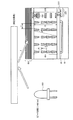
図1に本実施形態の分光センサーの構成例を示す。なお以下では、簡単のために本実施形態の構成を模式的に図示し、図中の寸法や比率は実際のものとは異なる。
角度制限フィルター40への入射光は、例えば青色LED300(広義には光源)の光を測定対象物に照射し、その測定対象物により反射又は散乱された光である。図2に、青色LED300のスペクトル(波長特性)例を示す。図2のF1にはプロセスバラツキのミニマムケース、F2にはティピカルケース、F3にはマックスケースを示す。図2に示すように、角度制限フィルター40に入射する可能性のある最短波長はλmin=410nmである。この場合、すき間の間隔は下式(2)に設定される。
光バンドパスフィルター60は、角度制限フィルター40の上に積層された多層薄膜により形成される。後述するように、角度制限フィルター40により入射角度が制限されることで光バンドパスフィルター60の透過波長帯域が制限され、所望の波長分解能の分光特性を得ることができる。
この工程の簡素化について比較例を用いて詳細に説明する。間隔b≦λ/2の条件で漏光が無いことについては後述する。
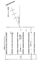
上述のように、すき間間隔がb≦λ/2を満たす場合には角度制限フィルターの側壁から漏光しないため、すき間領域が無い場合と同様の制限角度を得ることができる。この点について、図6〜図8を用いて説明する。
E−=sin(−kxcosβ+kxsinβ−ωt) (4)
ここで、βは、壁面に垂直な方向と光の進行方向との成す角度である。k=2π/λは光の波数である。x軸は、壁面に垂直な方向に沿った座標軸であり、Z軸は、x軸に垂直で壁面に平行な方向に沿った座標軸である。ωは光の各周波数である。tは時間である。
=2sin(kxcosβ)cos(kxsinβ−ωt) (5)
導体の壁面では境界条件E=0を満たす必要がある。壁面をx=0、bとすると、x=0ではE=0となり境界条件を満たす。x=bでは、sin(kxcosβ)=0の場合に境界条件を満たすため、下式(6)の角度βのみが許される。ここでnは自然数である。
b=λ/2とすると下式(7)となり、β=0°のみが許される。図8(B)に示すようにβ=0°では光が空間内を伝搬できないため、b≦λ/2では側壁のすき間から漏光しない。
=πcosβ
=nπ (7)
以上の実施形態によれば、すき間の間隔b≦λ/2では所望の制限角度が得られる。そして上述のように、このようなすき間を設けることでプロセスの簡素化を実現できる。
さて本実施形態では、角度制限フィルターの開口幅と高さを適切に設定することで、角度制御性や光到達率を高めることができる。この点について詳細に説明する。
また、制限角度θが下式(9)に示す条件を満たすように角度制限フィルター40が形成される。これは、角度制限フィルター40が無い場合であっても、入射光の入射角度が60°になるとフォトダイオード30に到達する光量が入射光量に対して1/2になるためである。即ち、到達光量が1/2になる入射角度を制限角度とする場合、角度制限フィルター40の角度制限を有効にするためにはθ<60°が必要である。
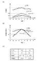
次に、上式(8)について、d2/(λ×R)<2の角度制限フィルターを比較例として説明する。図9(A)〜図9(C)に比較例の角度特性の測定値を示す。図9(A)〜図9(C)には、波長λ=0.5μm、高さR=5μmにおける測定値を示す。
d2/(λ×R)=3.642/(0.5×10)=2.65≧2 (11)
以上の実施形態によれば、角度制限フィルターの高さをRとし、角度制限フィルターの開口の幅をdとする場合に、d2/λR≧2を満たす。
上述した本実施形態の分光センサーの詳細な構成例について説明する。
される。後述するように、この傾斜構造体50は、例えばSiO2等の絶縁膜をエッチングまたはCMP、グレースケールリソグラフィー技術等により加工することで形成される。
上述のように、光バンドパスフィルターの透過波長帯域は、多層薄膜の傾斜角度と角度制限フィルターの制限角度により設定される。この点について、図13(A)、図13(B)を用いて具体的に説明する。なお、説明を簡単にするために、以下では光バンドパスフィルター61、62の多層薄膜の膜厚が同じ場合を例に説明するが、本実施形態では、光バンドパスフィルター61、62の多層薄膜の膜厚が傾斜角度θ1、θ2に応じて異なってもよい。例えば、薄膜のデポジションにおいて、半導体基板に対して垂直な方向に薄膜を成長させた場合、光バンドパスフィルター61、62の多層薄膜の膜厚がcosθ1、cosθ2に比例してもよい。
図14〜図16を用いて、傾斜構造体を半導体プロセスにより形成する場合の本実施形態の分光センサーの製造方法の例について説明する。
iO2の異方性ドライエッチング、フォトレジスト剥離の工程により、絶縁膜の段差(S9’)または粗密パターン(S9”)を形成する。
図17を用いて、傾斜構造体を別部材で形成する第1の変形例の製造方法の例について説明する。
図18に、本実施形態の光学センサーを含む電子機器の構成例を示す。例えば、電子機器として、脈拍計、パルスオキシメーター、血糖値測定器、果実糖度計などが想定される。なお本実施形態は図18の構成に限定されず、例えばLED950を省略して仰角測定装置や照度計等に用いてもよい。
40,41,42 角度制限フィルター、50 傾斜構造体、
60,61,62 光バンドパスフィルター、70 多層薄膜、
200 周辺回路、210 トランジスター、220 MIM型キャパシター、
221 上部電極、222 下部電極、230 配線、300 青色LED、
900 光学センサー装置、910 光学センサー、920 フォトダイオード、
930 検出回路、940 A/D変換回路、950 LED、
960 LEDドライバー、970 マイクロコンピューター、
980 記憶装置、990 表示装置、
ALA〜ALE,ALZ アルミ層、BW1,BW2 透過波長帯域、
HLA〜HLD,HLZ タングステンプラグ、HW 半値幅、
SLA〜SLD,SLZ 絶縁層、b 間隔、d 開口幅、α 入射角度、
θ,Δθ 制限角度、θ1,θ2 傾斜角度、λ 波長、λ1,λ2 透過波長
Claims (14)
- 半導体基板上に形成された、フォトダイオード用の不純物領域と、
前記フォトダイオードの受光領域に対する入射光の入射角度を制限する角度制限フィルターと、
を含み、
前記角度制限フィルターは、
少なくとも、第1の絶縁層に対応する第1のプラグと、前記第1の絶縁層よりも上層の第2の絶縁層に対応する第2のプラグにより形成され、
前記入射光の波長をλとする場合に、前記第1のプラグと前記第2のプラグの間には、すき間間隔がλ/2以下のすき間領域が設けられることを特徴とする光学センサー。 - 請求項1において、
前記第1の絶縁層は、
第1の金属層と、前記第1の金属層よりも上層の第2の金属層の間に設けられる絶縁層であり、
前記第2の絶縁層は、
前記第2の金属層と、前記第2の金属層よりも上層の第3の金属層の間に設けられる絶縁層であり、
前記第2の金属層は、
前記第1の金属層の厚さよりも厚い金属層であることを特徴とする光学センサー。 - 請求項2において、
前記フォトダイオードの出力信号を処理する回路であって、少なくとも前記第1〜第3の金属層と前記第1、第2のプラグにより配線が形成される処理回路を含み、
前記角度制限フィルターを形成する前記第1のプラグ及び前記第2のプラグは、
前記処理回路の配線層形成工程により形成されることを特徴とする光学センサー。 - 請求項3において、
前記処理回路は、
前記第2のプラグに対応する前記第2の絶縁層に形成されるMIM(Metal Insulator Metal)構造のキャパシターを有することを特徴とする光学センサー。 - 請求項4において、
前記MIM構造のキャパシターは、
前記第2の金属層を下部電極とし、前記第2の金属層と前記第3の金属層の間に形成される金属層を上部電極としたキャパシターであることを特徴とする光学センサー。 - 請求項1乃至5のいずれかにおいて、
前記角度制限フィルターを形成する前記第1のプラグ及び前記第2のプラグは、
前記フォトダイオード用の不純物領域の上に半導体プロセスによって形成された遮光物質であることを特徴とする光学センサー。 - 請求項1乃至6のいずれかにおいて、
前記角度制限フィルターの高さをRとし、前記角度制限フィルターの開口の幅をdとする場合に、
d2/λR≧2
を満たすことを特徴とする光学センサー。 - 請求項1乃至7のいずれかにおいて、
前記入射光のうちの特定波長の光を透過する光バンドパスフィルターを含むことを特徴とする光学センサー。 - 請求項8において、
前記光バンドパスフィルターは、
前記フォトダイオードの受光面に対して、透過波長に応じた角度で傾斜する多層薄膜により形成されることを特徴とする光学センサー。 - 請求項9において、
前記光バンドパスフィルターは、
透過波長が異なる複数組の多層薄膜により形成され、
前記複数組の多層薄膜は、
前記受光面に対する傾斜角度が透過波長に応じて異なり、同時の薄膜形成工程で形成されることを特徴とする光学センサー。 - 請求項1乃至10のいずれかにおいて、
前記入射光を分光するための分光センサーであることを特徴とする光学センサー。 - 請求項1乃至10のいずれかにおいて、
前記入射光の照度を測定するための照度センサーであることを特徴とする光学センサー。 - 請求項1乃至10のいずれかにおいて、
光源の仰角を測定するための仰角センサーであることを特徴とする光学センサー。 - 請求項1乃至13のいずれかに記載の光学センサーを含むことを特徴とする電子機器。
Priority Applications (2)
| Application Number | Priority Date | Filing Date | Title |
|---|---|---|---|
| JP2011058182A JP5810565B2 (ja) | 2011-03-16 | 2011-03-16 | 光学センサー及び電子機器 |
| US13/421,212 US8710606B2 (en) | 2011-03-16 | 2012-03-15 | Optical sensor and electronic apparatus |
Applications Claiming Priority (1)
| Application Number | Priority Date | Filing Date | Title |
|---|---|---|---|
| JP2011058182A JP5810565B2 (ja) | 2011-03-16 | 2011-03-16 | 光学センサー及び電子機器 |
Publications (2)
| Publication Number | Publication Date |
|---|---|
| JP2012194055A true JP2012194055A (ja) | 2012-10-11 |
| JP5810565B2 JP5810565B2 (ja) | 2015-11-11 |
Family
ID=46827807
Family Applications (1)
| Application Number | Title | Priority Date | Filing Date |
|---|---|---|---|
| JP2011058182A Active JP5810565B2 (ja) | 2011-03-16 | 2011-03-16 | 光学センサー及び電子機器 |
Country Status (2)
| Country | Link |
|---|---|
| US (1) | US8710606B2 (ja) |
| JP (1) | JP5810565B2 (ja) |
Cited By (4)
| Publication number | Priority date | Publication date | Assignee | Title |
|---|---|---|---|---|
| JP2016133510A (ja) * | 2015-01-16 | 2016-07-25 | パーソナル ジェノミクス タイワン インコーポレイテッドPersonal Genomics Taiwan,Inc. | 導光機能を有する光学センサー及びその製造方法 |
| US10838125B2 (en) | 2013-03-18 | 2020-11-17 | Seiko Epson Corporation | Interference filter, optical filter device, optical module, and electronic apparatus |
| CN114674788A (zh) * | 2016-06-01 | 2022-06-28 | 宽腾矽公司 | 用于检测及分析分子的集成装置 |
| WO2026021413A1 (zh) * | 2024-07-26 | 2026-01-29 | 华为技术有限公司 | 光检测器、颜色检测模组以及电子设备 |
Families Citing this family (5)
| Publication number | Priority date | Publication date | Assignee | Title |
|---|---|---|---|---|
| US9163984B2 (en) | 2011-03-17 | 2015-10-20 | Seiko Epson Corporation | Spectroscopic sensor and angle limiting filter |
| JP5803419B2 (ja) | 2011-08-19 | 2015-11-04 | セイコーエプソン株式会社 | 傾斜構造体、傾斜構造体の製造方法、及び分光センサー |
| EP2873953A1 (en) * | 2013-11-13 | 2015-05-20 | ams AG | Light sensor arrangement and spectrometer |
| JP2019133960A (ja) * | 2016-05-26 | 2019-08-08 | シャープ株式会社 | 光センサ |
| JP7715007B2 (ja) * | 2021-10-29 | 2025-07-30 | セイコーエプソン株式会社 | 検出装置および測定装置 |
Citations (7)
| Publication number | Priority date | Publication date | Assignee | Title |
|---|---|---|---|---|
| JPS6182230U (ja) * | 1984-11-02 | 1986-05-31 | ||
| JPH0894831A (ja) * | 1994-09-26 | 1996-04-12 | Olympus Optical Co Ltd | カラーフィルター |
| JP2001267544A (ja) * | 2000-03-21 | 2001-09-28 | Sharp Corp | 固体撮像装置およびその製造方法 |
| JP2005079513A (ja) * | 2003-09-03 | 2005-03-24 | Seiko Epson Corp | 半導体装置及びその製造方法 |
| JP2005294647A (ja) * | 2004-04-01 | 2005-10-20 | Matsushita Electric Ind Co Ltd | 固体撮像装置およびその製造方法 |
| JP2008153561A (ja) * | 2006-12-20 | 2008-07-03 | Seiko Epson Corp | 外部共振型レーザ光源装置及びそれを用いたモニタ装置並びに画像表示装置 |
| JP2011508232A (ja) * | 2007-12-26 | 2011-03-10 | コーニンクレッカ フィリップス エレクトロニクス エヌ ヴィ | マイクロ電子センサデバイス |
Family Cites Families (4)
| Publication number | Priority date | Publication date | Assignee | Title |
|---|---|---|---|---|
| JP2713838B2 (ja) | 1992-10-15 | 1998-02-16 | 浜松ホトニクス株式会社 | 分光イメージングセンサ |
| US7935994B2 (en) | 2005-02-24 | 2011-05-03 | Taiwan Semiconductor Manufacturing Company, Ltd. | Light shield for CMOS imager |
| JP4836498B2 (ja) | 2005-06-15 | 2011-12-14 | パナソニック株式会社 | 固体撮像装置及びカメラ |
| JP5663900B2 (ja) * | 2010-03-05 | 2015-02-04 | セイコーエプソン株式会社 | 分光センサー装置及び電子機器 |
-
2011
- 2011-03-16 JP JP2011058182A patent/JP5810565B2/ja active Active
-
2012
- 2012-03-15 US US13/421,212 patent/US8710606B2/en active Active
Patent Citations (7)
| Publication number | Priority date | Publication date | Assignee | Title |
|---|---|---|---|---|
| JPS6182230U (ja) * | 1984-11-02 | 1986-05-31 | ||
| JPH0894831A (ja) * | 1994-09-26 | 1996-04-12 | Olympus Optical Co Ltd | カラーフィルター |
| JP2001267544A (ja) * | 2000-03-21 | 2001-09-28 | Sharp Corp | 固体撮像装置およびその製造方法 |
| JP2005079513A (ja) * | 2003-09-03 | 2005-03-24 | Seiko Epson Corp | 半導体装置及びその製造方法 |
| JP2005294647A (ja) * | 2004-04-01 | 2005-10-20 | Matsushita Electric Ind Co Ltd | 固体撮像装置およびその製造方法 |
| JP2008153561A (ja) * | 2006-12-20 | 2008-07-03 | Seiko Epson Corp | 外部共振型レーザ光源装置及びそれを用いたモニタ装置並びに画像表示装置 |
| JP2011508232A (ja) * | 2007-12-26 | 2011-03-10 | コーニンクレッカ フィリップス エレクトロニクス エヌ ヴィ | マイクロ電子センサデバイス |
Cited By (7)
| Publication number | Priority date | Publication date | Assignee | Title |
|---|---|---|---|---|
| US10838125B2 (en) | 2013-03-18 | 2020-11-17 | Seiko Epson Corporation | Interference filter, optical filter device, optical module, and electronic apparatus |
| JP2016133510A (ja) * | 2015-01-16 | 2016-07-25 | パーソナル ジェノミクス タイワン インコーポレイテッドPersonal Genomics Taiwan,Inc. | 導光機能を有する光学センサー及びその製造方法 |
| JP2018054623A (ja) * | 2015-01-16 | 2018-04-05 | パーソナル ジェノミクス タイワン インコーポレイテッドPersonal Genomics Taiwan,Inc. | 導光機能を有する光学センサー及びその製造方法 |
| KR20180075454A (ko) * | 2015-01-16 | 2018-07-04 | 퍼스널 제노믹스 타이완, 아이엔씨. | 광-가이딩 피쳐를 갖는 광학 센서 그 제조 방법 |
| KR101994331B1 (ko) * | 2015-01-16 | 2019-09-30 | 퍼스널 제노믹스 타이완, 아이엔씨. | 광-가이딩 피쳐를 갖는 광학 센서 그 제조 방법 |
| CN114674788A (zh) * | 2016-06-01 | 2022-06-28 | 宽腾矽公司 | 用于检测及分析分子的集成装置 |
| WO2026021413A1 (zh) * | 2024-07-26 | 2026-01-29 | 华为技术有限公司 | 光检测器、颜色检测模组以及电子设备 |
Also Published As
| Publication number | Publication date |
|---|---|
| JP5810565B2 (ja) | 2015-11-11 |
| US20120235269A1 (en) | 2012-09-20 |
| US8710606B2 (en) | 2014-04-29 |
Similar Documents
| Publication | Publication Date | Title |
|---|---|---|
| JP5862025B2 (ja) | 光学センサー及び電子機器 | |
| JP5810565B2 (ja) | 光学センサー及び電子機器 | |
| JP6094652B2 (ja) | 光学センサー、電子機器及び脈拍計 | |
| JP6015034B2 (ja) | 光学センサー及び電子機器 | |
| JP5663900B2 (ja) | 分光センサー装置及び電子機器 | |
| JP5999168B2 (ja) | 光学センサー及び電子機器 | |
| CN102680094B (zh) | 分光传感器以及角度限制滤光器 | |
| JP5970685B2 (ja) | 光学センサー及び電子機器 | |
| JP6112190B2 (ja) | 分光センサー及びパルスオキシメーター | |
| JP5614339B2 (ja) | 分光センサー及び角度制限フィルター | |
| JP5862754B2 (ja) | 脈拍センサー及び脈拍計 | |
| JP5821400B2 (ja) | 分光センサー及び角度制限フィルター | |
| JP5614540B2 (ja) | 分光センサー及び角度制限フィルター | |
| JP5862753B2 (ja) | 分光センサー装置及び電子機器 | |
| JP5804166B2 (ja) | 分光センサー及び角度制限フィルター | |
| JP2016029374A (ja) | 分光センサー及び角度制限フィルター | |
| JP2013156325A (ja) | 分光センサー及び角度制限フィルター |
Legal Events
| Date | Code | Title | Description |
|---|---|---|---|
| A621 | Written request for application examination |
Free format text: JAPANESE INTERMEDIATE CODE: A621 Effective date: 20140305 |
|
| A977 | Report on retrieval |
Free format text: JAPANESE INTERMEDIATE CODE: A971007 Effective date: 20141014 |
|
| A131 | Notification of reasons for refusal |
Free format text: JAPANESE INTERMEDIATE CODE: A131 Effective date: 20141021 |
|
| A521 | Request for written amendment filed |
Free format text: JAPANESE INTERMEDIATE CODE: A523 Effective date: 20141219 |
|
| A131 | Notification of reasons for refusal |
Free format text: JAPANESE INTERMEDIATE CODE: A131 Effective date: 20150512 |
|
| A521 | Request for written amendment filed |
Free format text: JAPANESE INTERMEDIATE CODE: A523 Effective date: 20150710 |
|
| TRDD | Decision of grant or rejection written | ||
| A01 | Written decision to grant a patent or to grant a registration (utility model) |
Free format text: JAPANESE INTERMEDIATE CODE: A01 Effective date: 20150818 |
|
| A61 | First payment of annual fees (during grant procedure) |
Free format text: JAPANESE INTERMEDIATE CODE: A61 Effective date: 20150831 |
|
| R150 | Certificate of patent or registration of utility model |
Ref document number: 5810565 Country of ref document: JP Free format text: JAPANESE INTERMEDIATE CODE: R150 |
|
| S531 | Written request for registration of change of domicile |
Free format text: JAPANESE INTERMEDIATE CODE: R313531 |
|
| R350 | Written notification of registration of transfer |
Free format text: JAPANESE INTERMEDIATE CODE: R350 |