JP2012194080A - ボロメータ型THz波検出器 - Google Patents
ボロメータ型THz波検出器 Download PDFInfo
- Publication number
- JP2012194080A JP2012194080A JP2011058693A JP2011058693A JP2012194080A JP 2012194080 A JP2012194080 A JP 2012194080A JP 2011058693 A JP2011058693 A JP 2011058693A JP 2011058693 A JP2011058693 A JP 2011058693A JP 2012194080 A JP2012194080 A JP 2012194080A
- Authority
- JP
- Japan
- Prior art keywords
- film
- thz wave
- bolometer
- temperature detection
- wave detector
- Prior art date
- Legal status (The legal status is an assumption and is not a legal conclusion. Google has not performed a legal analysis and makes no representation as to the accuracy of the status listed.)
- Pending
Links
- 239000010408 film Substances 0.000 claims abstract description 200
- 239000010409 thin film Substances 0.000 claims abstract description 24
- 239000000758 substrate Substances 0.000 claims abstract description 13
- 230000003287 optical effect Effects 0.000 claims abstract description 9
- 238000009429 electrical wiring Methods 0.000 claims abstract description 8
- 238000001514 detection method Methods 0.000 claims description 53
- 238000010521 absorption reaction Methods 0.000 claims description 38
- 230000002093 peripheral effect Effects 0.000 claims description 4
- 238000004519 manufacturing process Methods 0.000 abstract description 20
- 238000002955 isolation Methods 0.000 abstract 1
- 230000001681 protective effect Effects 0.000 description 95
- 239000010410 layer Substances 0.000 description 27
- 229910052581 Si3N4 Inorganic materials 0.000 description 13
- HQVNEWCFYHHQES-UHFFFAOYSA-N silicon nitride Chemical compound N12[Si]34N5[Si]62N3[Si]51N64 HQVNEWCFYHHQES-UHFFFAOYSA-N 0.000 description 13
- 229920001721 polyimide Polymers 0.000 description 9
- VYPSYNLAJGMNEJ-UHFFFAOYSA-N Silicium dioxide Chemical compound O=[Si]=O VYPSYNLAJGMNEJ-UHFFFAOYSA-N 0.000 description 8
- 238000010586 diagram Methods 0.000 description 8
- 229910052751 metal Inorganic materials 0.000 description 8
- 239000002184 metal Substances 0.000 description 8
- 229910052814 silicon oxide Inorganic materials 0.000 description 8
- 239000004642 Polyimide Substances 0.000 description 7
- 229910052782 aluminium Inorganic materials 0.000 description 7
- 239000000463 material Substances 0.000 description 7
- 239000010936 titanium Substances 0.000 description 7
- 229910052719 titanium Inorganic materials 0.000 description 7
- 229910004298 SiO 2 Inorganic materials 0.000 description 6
- XUIMIQQOPSSXEZ-UHFFFAOYSA-N Silicon Chemical compound [Si] XUIMIQQOPSSXEZ-UHFFFAOYSA-N 0.000 description 6
- 230000002950 deficient Effects 0.000 description 6
- 238000010438 heat treatment Methods 0.000 description 6
- 229910052710 silicon Inorganic materials 0.000 description 6
- 239000010703 silicon Substances 0.000 description 6
- LIVNPJMFVYWSIS-UHFFFAOYSA-N silicon monoxide Chemical compound [Si-]#[O+] LIVNPJMFVYWSIS-UHFFFAOYSA-N 0.000 description 6
- 239000007789 gas Substances 0.000 description 5
- 238000004544 sputter deposition Methods 0.000 description 5
- NBIIXXVUZAFLBC-UHFFFAOYSA-N Phosphoric acid Chemical compound OP(O)(O)=O NBIIXXVUZAFLBC-UHFFFAOYSA-N 0.000 description 4
- 238000004364 calculation method Methods 0.000 description 4
- 238000000151 deposition Methods 0.000 description 4
- 238000000034 method Methods 0.000 description 4
- 238000005268 plasma chemical vapour deposition Methods 0.000 description 4
- 230000007261 regionalization Effects 0.000 description 4
- WGTYBPLFGIVFAS-UHFFFAOYSA-M tetramethylammonium hydroxide Chemical compound [OH-].C[N+](C)(C)C WGTYBPLFGIVFAS-UHFFFAOYSA-M 0.000 description 4
- 238000001039 wet etching Methods 0.000 description 4
- 238000004380 ashing Methods 0.000 description 3
- QVGXLLKOCUKJST-UHFFFAOYSA-N atomic oxygen Chemical compound [O] QVGXLLKOCUKJST-UHFFFAOYSA-N 0.000 description 3
- 230000015572 biosynthetic process Effects 0.000 description 3
- 230000018109 developmental process Effects 0.000 description 3
- 239000011810 insulating material Substances 0.000 description 3
- 239000001301 oxygen Substances 0.000 description 3
- 229910052760 oxygen Inorganic materials 0.000 description 3
- OGIDPMRJRNCKJF-UHFFFAOYSA-N titanium oxide Inorganic materials [Ti]=O OGIDPMRJRNCKJF-UHFFFAOYSA-N 0.000 description 3
- KRHYYFGTRYWZRS-UHFFFAOYSA-N Fluorane Chemical compound F KRHYYFGTRYWZRS-UHFFFAOYSA-N 0.000 description 2
- OAKJQQAXSVQMHS-UHFFFAOYSA-N Hydrazine Chemical compound NN OAKJQQAXSVQMHS-UHFFFAOYSA-N 0.000 description 2
- VEXZGXHMUGYJMC-UHFFFAOYSA-N Hydrochloric acid Chemical compound Cl VEXZGXHMUGYJMC-UHFFFAOYSA-N 0.000 description 2
- GWEVSGVZZGPLCZ-UHFFFAOYSA-N Titan oxide Chemical compound O=[Ti]=O GWEVSGVZZGPLCZ-UHFFFAOYSA-N 0.000 description 2
- XHCLAFWTIXFWPH-UHFFFAOYSA-N [O-2].[O-2].[O-2].[O-2].[O-2].[V+5].[V+5] Chemical compound [O-2].[O-2].[O-2].[O-2].[O-2].[V+5].[V+5] XHCLAFWTIXFWPH-UHFFFAOYSA-N 0.000 description 2
- 229910000147 aluminium phosphate Inorganic materials 0.000 description 2
- NBVXSUQYWXRMNV-UHFFFAOYSA-N monofluoromethane Natural products FC NBVXSUQYWXRMNV-UHFFFAOYSA-N 0.000 description 2
- 238000001020 plasma etching Methods 0.000 description 2
- 229910021420 polycrystalline silicon Inorganic materials 0.000 description 2
- 229920005591 polysilicon Polymers 0.000 description 2
- 239000004065 semiconductor Substances 0.000 description 2
- 230000035945 sensitivity Effects 0.000 description 2
- 238000000926 separation method Methods 0.000 description 2
- 229910001935 vanadium oxide Inorganic materials 0.000 description 2
- 229910052802 copper Inorganic materials 0.000 description 1
- 238000005336 cracking Methods 0.000 description 1
- 230000007547 defect Effects 0.000 description 1
- 239000003989 dielectric material Substances 0.000 description 1
- 238000001312 dry etching Methods 0.000 description 1
- 230000000694 effects Effects 0.000 description 1
- 238000005516 engineering process Methods 0.000 description 1
- 229910052737 gold Inorganic materials 0.000 description 1
- 238000003384 imaging method Methods 0.000 description 1
- 238000009413 insulation Methods 0.000 description 1
- 239000011229 interlayer Substances 0.000 description 1
- UUXZFMKOCRKVDG-UHFFFAOYSA-N methane;hydrofluoride Chemical compound C.F UUXZFMKOCRKVDG-UHFFFAOYSA-N 0.000 description 1
- 239000011241 protective layer Substances 0.000 description 1
- 238000005546 reactive sputtering Methods 0.000 description 1
- 229910052721 tungsten Inorganic materials 0.000 description 1
Images


Classifications
-
- G—PHYSICS
- G01—MEASURING; TESTING
- G01J—MEASUREMENT OF INTENSITY, VELOCITY, SPECTRAL CONTENT, POLARISATION, PHASE OR PULSE CHARACTERISTICS OF INFRARED, VISIBLE OR ULTRAVIOLET LIGHT; COLORIMETRY; RADIATION PYROMETRY
- G01J5/00—Radiation pyrometry, e.g. infrared or optical thermometry
- G01J5/02—Constructional details
- G01J5/04—Casings
- G01J5/041—Mountings in enclosures or in a particular environment
- G01J5/045—Sealings; Vacuum enclosures; Encapsulated packages; Wafer bonding structures; Getter arrangements
-
- G—PHYSICS
- G01—MEASURING; TESTING
- G01J—MEASUREMENT OF INTENSITY, VELOCITY, SPECTRAL CONTENT, POLARISATION, PHASE OR PULSE CHARACTERISTICS OF INFRARED, VISIBLE OR ULTRAVIOLET LIGHT; COLORIMETRY; RADIATION PYROMETRY
- G01J5/00—Radiation pyrometry, e.g. infrared or optical thermometry
- G01J5/02—Constructional details
- G01J5/0215—Compact construction
-
- G—PHYSICS
- G01—MEASURING; TESTING
- G01J—MEASUREMENT OF INTENSITY, VELOCITY, SPECTRAL CONTENT, POLARISATION, PHASE OR PULSE CHARACTERISTICS OF INFRARED, VISIBLE OR ULTRAVIOLET LIGHT; COLORIMETRY; RADIATION PYROMETRY
- G01J5/00—Radiation pyrometry, e.g. infrared or optical thermometry
- G01J5/02—Constructional details
- G01J5/0225—Shape of the cavity itself or of elements contained in or suspended over the cavity
-
- G—PHYSICS
- G01—MEASURING; TESTING
- G01J—MEASUREMENT OF INTENSITY, VELOCITY, SPECTRAL CONTENT, POLARISATION, PHASE OR PULSE CHARACTERISTICS OF INFRARED, VISIBLE OR ULTRAVIOLET LIGHT; COLORIMETRY; RADIATION PYROMETRY
- G01J5/00—Radiation pyrometry, e.g. infrared or optical thermometry
- G01J5/02—Constructional details
- G01J5/0225—Shape of the cavity itself or of elements contained in or suspended over the cavity
- G01J5/024—Special manufacturing steps or sacrificial layers or layer structures
-
- G—PHYSICS
- G01—MEASURING; TESTING
- G01J—MEASUREMENT OF INTENSITY, VELOCITY, SPECTRAL CONTENT, POLARISATION, PHASE OR PULSE CHARACTERISTICS OF INFRARED, VISIBLE OR ULTRAVIOLET LIGHT; COLORIMETRY; RADIATION PYROMETRY
- G01J5/00—Radiation pyrometry, e.g. infrared or optical thermometry
- G01J5/02—Constructional details
- G01J5/06—Arrangements for eliminating effects of disturbing radiation; Arrangements for compensating changes in sensitivity
-
- G—PHYSICS
- G01—MEASURING; TESTING
- G01J—MEASUREMENT OF INTENSITY, VELOCITY, SPECTRAL CONTENT, POLARISATION, PHASE OR PULSE CHARACTERISTICS OF INFRARED, VISIBLE OR ULTRAVIOLET LIGHT; COLORIMETRY; RADIATION PYROMETRY
- G01J5/00—Radiation pyrometry, e.g. infrared or optical thermometry
- G01J5/02—Constructional details
- G01J5/08—Optical arrangements
- G01J5/0853—Optical arrangements having infrared absorbers other than the usual absorber layers deposited on infrared detectors like bolometers, wherein the heat propagation between the absorber and the detecting element occurs within a solid
-
- G—PHYSICS
- G01—MEASURING; TESTING
- G01J—MEASUREMENT OF INTENSITY, VELOCITY, SPECTRAL CONTENT, POLARISATION, PHASE OR PULSE CHARACTERISTICS OF INFRARED, VISIBLE OR ULTRAVIOLET LIGHT; COLORIMETRY; RADIATION PYROMETRY
- G01J5/00—Radiation pyrometry, e.g. infrared or optical thermometry
- G01J5/10—Radiation pyrometry, e.g. infrared or optical thermometry using electric radiation detectors
- G01J5/20—Radiation pyrometry, e.g. infrared or optical thermometry using electric radiation detectors using resistors, thermistors or semiconductors sensitive to radiation, e.g. photoconductive devices
Landscapes
- Physics & Mathematics (AREA)
- General Physics & Mathematics (AREA)
- Spectroscopy & Molecular Physics (AREA)
- Engineering & Computer Science (AREA)
- Manufacturing & Machinery (AREA)
- Photometry And Measurement Of Optical Pulse Characteristics (AREA)
- Solid State Image Pick-Up Elements (AREA)
Abstract
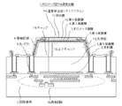
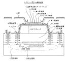
【解決手段】基板に形成された読出回路に接続される電気配線を含む支持部により、前記電気配線に接続されるボロメータ薄膜を含む温度検出部が、前記基板から浮いた状態で支持される熱分離構造を有するボロメータ型THz波検出器であって、前記基板上の前記温度検出部に対向する位置にTHz波を反射する反射膜が形成され、前記温度検出部の表面、裏面あるいは内部に前記THz波を吸収する吸収膜が形成され、前記反射膜と前記吸収膜とで光学的共振構造が形成され、前記反射膜上にTHz波に対して透明な誘電体が形成され、前記誘電体の上面と前記温度検出部の下面との間隔(エアギャップ)が8μm未満となるように、前記誘電体の膜厚が設定されている。
【選択図】図1
Description
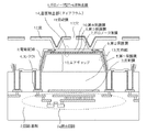
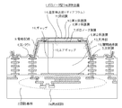
2 回路基板
2a 読出回路
3 反射膜
4 コンタクト
5 第1保護膜
6 第2保護膜
7 ボロメータ薄膜
8 第3保護膜
9 電極配線
10 第4保護膜
11 吸収膜
12 庇
13 支持部
14 温度検出部(ダイアフラム)
15 エアギャップ
16 ギャップ
17 穴
18 層間絶縁膜
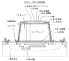
20 従来のボロメータ型THz波検出器
Claims (4)
- 基板に形成された読出回路に接続される電気配線を含む支持部により、前記電気配線に接続されるボロメータ薄膜を含む温度検出部が、前記基板から浮いた状態で支持される熱分離構造を有するボロメータ型THz波検出器であって、
前記基板上の前記温度検出部に対向する位置にTHz波を反射する反射膜が形成され、前記温度検出部の表面、裏面あるいは内部に前記THz波を吸収する吸収膜が形成され、前記反射膜と前記吸収膜とで光学的共振構造が形成され、
前記反射膜上にTHz波に対して透明な誘電体が形成され、
前記誘電体の上面と前記温度検出部の下面との間隔が8μm未満となるように、前記誘電体の膜厚が設定されていることを特徴とするボロメータ型THz波検出器。 - 更に、前記温度検出部上に、該温度検出部の周縁部から外側に延びる庇が形成され、前記吸収膜が、前記温度検出部の表面、裏面あるいは内部、及び前記庇の表面、裏面あるいは内部に形成されていることを特徴とする請求項1に記載のボロメータ型THz波検出器。
- 更に、前記温度検出部上に、該温度検出部の周縁部から内側及び外側に延びる庇が形成され、前記吸収膜が、前記庇の表面、裏面あるいは内部に形成されることを特徴とする請求項1に記載のボロメータ型THz波検出器。
- 前記読出回路と前記電気配線とが、前記誘電体内に形成された多層配線により接続されることを特徴とする請求項1乃至3のいずれか一に記載のボロメータ型THz波検出器。
Priority Applications (2)
| Application Number | Priority Date | Filing Date | Title |
|---|---|---|---|
| JP2011058693A JP2012194080A (ja) | 2011-03-17 | 2011-03-17 | ボロメータ型THz波検出器 |
| US13/422,120 US8541742B2 (en) | 2011-03-17 | 2012-03-16 | Bolometer-type THz wave detector |
Applications Claiming Priority (1)
| Application Number | Priority Date | Filing Date | Title |
|---|---|---|---|
| JP2011058693A JP2012194080A (ja) | 2011-03-17 | 2011-03-17 | ボロメータ型THz波検出器 |
Publications (1)
| Publication Number | Publication Date |
|---|---|
| JP2012194080A true JP2012194080A (ja) | 2012-10-11 |
Family
ID=46827730
Family Applications (1)
| Application Number | Title | Priority Date | Filing Date |
|---|---|---|---|
| JP2011058693A Pending JP2012194080A (ja) | 2011-03-17 | 2011-03-17 | ボロメータ型THz波検出器 |
Country Status (2)
| Country | Link |
|---|---|
| US (1) | US8541742B2 (ja) |
| JP (1) | JP2012194080A (ja) |
Cited By (6)
| Publication number | Priority date | Publication date | Assignee | Title |
|---|---|---|---|---|
| WO2017077996A1 (ja) * | 2015-11-04 | 2017-05-11 | 日本電気株式会社 | ボロメータ型テラヘルツ波検出器 |
| WO2017094280A1 (ja) * | 2015-11-30 | 2017-06-08 | 国立大学法人東京大学 | ボロメータ型テラヘルツ波検出素子およびボロメータ型テラヘルツ波検出素子アレイ |
| KR20170105534A (ko) * | 2015-01-08 | 2017-09-19 | 플리어 시스템즈, 인크. | 적외선 기준 화소를 위한 장치 및 방법 |
| KR20210052971A (ko) * | 2019-11-01 | 2021-05-11 | 주식회사 트루윈 | 마이크로 볼로미터 및 마이크로 볼로미터 제조 방법 |
| KR20210114174A (ko) * | 2020-03-10 | 2021-09-23 | 한국과학기술원 | 볼로미터 멤스 소자 및 볼로미터 멤스 소자의 제조 방법 |
| JP2023033863A (ja) * | 2021-08-30 | 2023-03-13 | Tdk株式会社 | 構造体及び電磁波センサ |
Families Citing this family (11)
| Publication number | Priority date | Publication date | Assignee | Title |
|---|---|---|---|---|
| US9029773B2 (en) * | 2013-02-24 | 2015-05-12 | Vlad Novotny | Sealed infrared imagers |
| CN103193190B (zh) * | 2013-04-11 | 2015-07-29 | 电子科技大学 | 一种红外-太赫兹双波段阵列探测器微桥结构及其制备方法 |
| JP2014235146A (ja) * | 2013-06-05 | 2014-12-15 | セイコーエプソン株式会社 | テラヘルツ波検出装置、カメラ、イメージング装置および計測装置 |
| JP2014235144A (ja) * | 2013-06-05 | 2014-12-15 | セイコーエプソン株式会社 | テラヘルツ波検出装置、カメラ、イメージング装置および計測装置 |
| US9377350B2 (en) * | 2014-09-04 | 2016-06-28 | Newport Fab, Llc | Light sensor with chemically resistant and robust reflector stack |
| CN106115604B (zh) * | 2016-07-25 | 2018-09-28 | 电子科技大学 | 基于超材料结构的太赫兹微测辐射热计及其制备方法 |
| US10825857B2 (en) * | 2016-09-29 | 2020-11-03 | Yantai Raytron Technology Co., Ltd | Pixel for uncooled infrared focal plane detector and preparation method therefor |
| JP6726087B2 (ja) * | 2016-12-14 | 2020-07-22 | 浜松ホトニクス株式会社 | 光検出器 |
| US10199424B1 (en) * | 2017-07-19 | 2019-02-05 | Meridian Innovation Pte Ltd | Thermoelectric-based infrared detector having a cavity and a MEMS structure defined by BEOL metals lines |
| FR3081989B1 (fr) * | 2018-05-30 | 2020-08-21 | Commissariat Energie Atomique | Systeme de detection a pixel sensible comportant un detecteur thermique et un dispositif de compensation |
| CN109659707B (zh) * | 2018-12-24 | 2021-03-09 | 广东工业大学 | 基于n×m介质谐振天线阵列的太赫兹探测器和方法 |
Citations (5)
| Publication number | Priority date | Publication date | Assignee | Title |
|---|---|---|---|---|
| JPH11317500A (ja) * | 1998-03-04 | 1999-11-16 | Nec Corp | 容量素子を有する半導体装置及びその製造方法 |
| JP2006324265A (ja) * | 2005-05-17 | 2006-11-30 | Matsushita Electric Ind Co Ltd | 半導体装置 |
| JP2008241438A (ja) * | 2007-03-27 | 2008-10-09 | Nec Corp | ボロメータ型THz波検出器 |
| JP2009216558A (ja) * | 2008-03-11 | 2009-09-24 | Oki Semiconductor Co Ltd | 赤外線検出素子の製造方法 |
| JP2010261935A (ja) * | 2009-04-30 | 2010-11-18 | Commissariat A L'energie Atomique & Aux Energies Alternatives | 赤外からテラヘルツ周波数帯域の電磁放射を検出するボロメータ検出器、およびかかる検出器を備えたアレイ検出装置 |
-
2011
- 2011-03-17 JP JP2011058693A patent/JP2012194080A/ja active Pending
-
2012
- 2012-03-16 US US13/422,120 patent/US8541742B2/en active Active
Patent Citations (5)
| Publication number | Priority date | Publication date | Assignee | Title |
|---|---|---|---|---|
| JPH11317500A (ja) * | 1998-03-04 | 1999-11-16 | Nec Corp | 容量素子を有する半導体装置及びその製造方法 |
| JP2006324265A (ja) * | 2005-05-17 | 2006-11-30 | Matsushita Electric Ind Co Ltd | 半導体装置 |
| JP2008241438A (ja) * | 2007-03-27 | 2008-10-09 | Nec Corp | ボロメータ型THz波検出器 |
| JP2009216558A (ja) * | 2008-03-11 | 2009-09-24 | Oki Semiconductor Co Ltd | 赤外線検出素子の製造方法 |
| JP2010261935A (ja) * | 2009-04-30 | 2010-11-18 | Commissariat A L'energie Atomique & Aux Energies Alternatives | 赤外からテラヘルツ周波数帯域の電磁放射を検出するボロメータ検出器、およびかかる検出器を備えたアレイ検出装置 |
Cited By (15)
| Publication number | Priority date | Publication date | Assignee | Title |
|---|---|---|---|---|
| KR20170105534A (ko) * | 2015-01-08 | 2017-09-19 | 플리어 시스템즈, 인크. | 적외선 기준 화소를 위한 장치 및 방법 |
| KR102411749B1 (ko) | 2015-01-08 | 2022-06-22 | 텔레다인 플리어, 엘엘시 | 적외선 기준 화소를 위한 장치 및 방법 |
| WO2017077996A1 (ja) * | 2015-11-04 | 2017-05-11 | 日本電気株式会社 | ボロメータ型テラヘルツ波検出器 |
| JPWO2017077996A1 (ja) * | 2015-11-04 | 2018-08-23 | 日本電気株式会社 | ボロメータ型テラヘルツ波検出器 |
| WO2017094280A1 (ja) * | 2015-11-30 | 2017-06-08 | 国立大学法人東京大学 | ボロメータ型テラヘルツ波検出素子およびボロメータ型テラヘルツ波検出素子アレイ |
| JPWO2017094280A1 (ja) * | 2015-11-30 | 2018-09-13 | 国立大学法人 東京大学 | ボロメータ型テラヘルツ波検出素子およびボロメータ型テラヘルツ波検出素子アレイ |
| KR102286307B1 (ko) * | 2019-11-01 | 2021-08-05 | 주식회사 트루윈 | 마이크로 볼로미터 및 마이크로 볼로미터 제조 방법 |
| KR20210052971A (ko) * | 2019-11-01 | 2021-05-11 | 주식회사 트루윈 | 마이크로 볼로미터 및 마이크로 볼로미터 제조 방법 |
| KR20210114174A (ko) * | 2020-03-10 | 2021-09-23 | 한국과학기술원 | 볼로미터 멤스 소자 및 볼로미터 멤스 소자의 제조 방법 |
| WO2021182813A3 (ko) * | 2020-03-10 | 2021-11-11 | 한국과학기술원 | 볼로미터 멤스 소자 및 볼로미터 멤스 소자의 제조 방법 |
| KR102358860B1 (ko) * | 2020-03-10 | 2022-02-07 | 한국과학기술원 | 볼로미터 멤스 소자 및 볼로미터 멤스 소자의 제조 방법 |
| KR20220019739A (ko) * | 2020-03-10 | 2022-02-17 | 한국과학기술원 | 볼로미터 멤스 소자 및 볼로미터 멤스 소자의 제조 방법 |
| KR102587111B1 (ko) * | 2020-03-10 | 2023-10-12 | 한국과학기술원 | 볼로미터 멤스 소자 및 볼로미터 멤스 소자의 제조 방법 |
| JP2023033863A (ja) * | 2021-08-30 | 2023-03-13 | Tdk株式会社 | 構造体及び電磁波センサ |
| JP7718914B2 (ja) | 2021-08-30 | 2025-08-05 | Tdk株式会社 | 構造体及び電磁波センサ |
Also Published As
| Publication number | Publication date |
|---|---|
| US20120235045A1 (en) | 2012-09-20 |
| US8541742B2 (en) | 2013-09-24 |
Similar Documents
| Publication | Publication Date | Title |
|---|---|---|
| US8541742B2 (en) | Bolometer-type THz wave detector | |
| JP5964543B2 (ja) | ボロメータ型テラヘルツ波検出器 | |
| JP5597862B2 (ja) | ボロメータ型THz波検出器 | |
| JP5109169B2 (ja) | ボロメータ型THz波検出器 | |
| KR100925214B1 (ko) | 볼로미터 및 그 제조 방법 | |
| US9222837B2 (en) | Black silicon-based high-performance MEMS thermopile IR detector and fabrication method | |
| JP5428783B2 (ja) | ボロメータ型THz波検出器 | |
| JP5801151B2 (ja) | 懸架式ボロメータマイクロプレートに基づく赤外線検出器 | |
| EP3522217B1 (en) | Method to prepare pixel for uncooled infrared focal plane detector | |
| US7928388B2 (en) | Infrared detection sensor and method of fabricating the same | |
| CN109813447B (zh) | 集成宽带人工表面的非制冷红外焦平面及制作方法 | |
| CN103193190B (zh) | 一种红外-太赫兹双波段阵列探测器微桥结构及其制备方法 | |
| WO2005034248A1 (en) | Bolometric infrared sensor having two layer structure and method for manufacturing the same | |
| JP2009192350A (ja) | 熱型赤外線検出器及びその製造方法 | |
| JP2005116856A (ja) | 熱型赤外線固体撮像素子及びその製造方法 | |
| US20250185393A1 (en) | Methods and systems for fabrication of infrared transparent window wafer with integrated anti-reflection grating structures | |
| CN107478336B (zh) | 太赫兹成像阵列芯片及其制作方法、成像系统 | |
| KR100509443B1 (ko) | 2층 구조의 볼로미터형 적외선 센서 및 그 제조방법 | |
| JP5264471B2 (ja) | 赤外線検出器および赤外線固体撮像装置 | |
| KR100715112B1 (ko) | 2층 구조의 비냉각형 적외선 센서 및 그 제조방법 | |
| KR100502577B1 (ko) | 2층 구조의 볼로미터형 적외선 센서 | |
| TWI809668B (zh) | 微機電紅外光感測裝置及其製造方法 | |
| CN105174206B (zh) | 一种电极引线及微桥结构中的电极引线的制备方法 | |
| KR20260043781A (ko) | 메타표면 구조를 가지는 복층구조의 마이크로볼로미터 센서 | |
| KR20090103842A (ko) | 열형 적외선 고체 촬상 소자 및 그 제조 방법 |
Legal Events
| Date | Code | Title | Description |
|---|---|---|---|
| A621 | Written request for application examination |
Free format text: JAPANESE INTERMEDIATE CODE: A621 Effective date: 20130919 |
|
| A977 | Report on retrieval |
Free format text: JAPANESE INTERMEDIATE CODE: A971007 Effective date: 20140226 |
|
| A131 | Notification of reasons for refusal |
Free format text: JAPANESE INTERMEDIATE CODE: A131 Effective date: 20140902 |
|
| A521 | Request for written amendment filed |
Free format text: JAPANESE INTERMEDIATE CODE: A523 Effective date: 20141023 |
|
| A02 | Decision of refusal |
Free format text: JAPANESE INTERMEDIATE CODE: A02 Effective date: 20150303 |
|
| A521 | Request for written amendment filed |
Free format text: JAPANESE INTERMEDIATE CODE: A523 Effective date: 20150602 |
|
| A911 | Transfer to examiner for re-examination before appeal (zenchi) |
Free format text: JAPANESE INTERMEDIATE CODE: A911 Effective date: 20150609 |
|
| A912 | Re-examination (zenchi) completed and case transferred to appeal board |
Free format text: JAPANESE INTERMEDIATE CODE: A912 Effective date: 20150828 |