JP2012194272A - Toner density sensor and image forming device - Google Patents
Toner density sensor and image forming device Download PDFInfo
- Publication number
- JP2012194272A JP2012194272A JP2011056991A JP2011056991A JP2012194272A JP 2012194272 A JP2012194272 A JP 2012194272A JP 2011056991 A JP2011056991 A JP 2011056991A JP 2011056991 A JP2011056991 A JP 2011056991A JP 2012194272 A JP2012194272 A JP 2012194272A
- Authority
- JP
- Japan
- Prior art keywords
- light
- light emitting
- light receiving
- space
- emitting element
- Prior art date
- Legal status (The legal status is an assumption and is not a legal conclusion. Google has not performed a legal analysis and makes no representation as to the accuracy of the status listed.)
- Granted
Links
Images





Classifications
-
- G—PHYSICS
- G03—PHOTOGRAPHY; CINEMATOGRAPHY; ANALOGOUS TECHNIQUES USING WAVES OTHER THAN OPTICAL WAVES; ELECTROGRAPHY; HOLOGRAPHY
- G03G—ELECTROGRAPHY; ELECTROPHOTOGRAPHY; MAGNETOGRAPHY
- G03G15/00—Apparatus for electrographic processes using a charge pattern
- G03G15/50—Machine control of apparatus for electrographic processes using a charge pattern, e.g. regulating differents parts of the machine, multimode copiers, microprocessor control
- G03G15/5054—Machine control of apparatus for electrographic processes using a charge pattern, e.g. regulating differents parts of the machine, multimode copiers, microprocessor control by measuring the characteristics of an intermediate image carrying member or the characteristics of an image on an intermediate image carrying member, e.g. intermediate transfer belt or drum, conveyor belt
- G03G15/5058—Machine control of apparatus for electrographic processes using a charge pattern, e.g. regulating differents parts of the machine, multimode copiers, microprocessor control by measuring the characteristics of an intermediate image carrying member or the characteristics of an image on an intermediate image carrying member, e.g. intermediate transfer belt or drum, conveyor belt using a test patch
-
- G—PHYSICS
- G03—PHOTOGRAPHY; CINEMATOGRAPHY; ANALOGOUS TECHNIQUES USING WAVES OTHER THAN OPTICAL WAVES; ELECTROGRAPHY; HOLOGRAPHY
- G03G—ELECTROGRAPHY; ELECTROPHOTOGRAPHY; MAGNETOGRAPHY
- G03G15/00—Apparatus for electrographic processes using a charge pattern
- G03G15/06—Apparatus for electrographic processes using a charge pattern for developing
- G03G15/08—Apparatus for electrographic processes using a charge pattern for developing using a solid developer, e.g. powder developer
-
- G—PHYSICS
- G03—PHOTOGRAPHY; CINEMATOGRAPHY; ANALOGOUS TECHNIQUES USING WAVES OTHER THAN OPTICAL WAVES; ELECTROGRAPHY; HOLOGRAPHY
- G03G—ELECTROGRAPHY; ELECTROPHOTOGRAPHY; MAGNETOGRAPHY
- G03G15/00—Apparatus for electrographic processes using a charge pattern
- G03G15/01—Apparatus for electrographic processes using a charge pattern for producing multicoloured copies
- G03G15/0142—Structure of complete machines
- G03G15/0178—Structure of complete machines using more than one reusable electrographic recording member, e.g. one for every monocolour image
- G03G15/0194—Structure of complete machines using more than one reusable electrographic recording member, e.g. one for every monocolour image primary transfer to the final recording medium
Landscapes
- Physics & Mathematics (AREA)
- General Physics & Mathematics (AREA)
- Engineering & Computer Science (AREA)
- Microelectronics & Electronic Packaging (AREA)
- Investigating Or Analysing Materials By Optical Means (AREA)
- Photometry And Measurement Of Optical Pulse Characteristics (AREA)
- Electrostatic Charge, Transfer And Separation In Electrography (AREA)
- Control Or Security For Electrophotography (AREA)
- Color Electrophotography (AREA)
- Electrophotography Configuration And Component (AREA)
Abstract
【課題】画像形成装置に搭載されるトナー濃度センサにおいて、基板に表面実装された発光素子と受光素子の距離が近い小型の場合でも、基板内を伝播するノイズ光によって検出精度の劣化が起きるのを良好に抑制する。
【解決手段】トナー濃度を検出するために光を照射する発光素子12と、該発光素子12から照射されて検出対象で反射した反射光を受光する受光素子13,14をプリント基板15上に表面実装したトナー濃度センサ11において、前記プリント基板15における前記発光素子12の取り付け部分に、厚み方向に貫く貫通空間部21を形成する。発光素子12からプリント基板15方向に照射された照射光L3のほとんどは外部に放射されるので、プリント基板15内に伝播するノイズ光の発生を抑制できる。
【選択図】図4In a toner concentration sensor mounted on an image forming apparatus, even when the distance between a light emitting element and a light receiving element mounted on the surface of a substrate is small, detection accuracy deteriorates due to noise light propagating in the substrate. Is suppressed well.
A light emitting element that emits light to detect a toner density, and light receiving elements that receive reflected light reflected from a detection target irradiated from the light emitting element are provided on a surface of the printed circuit board. In the mounted toner density sensor 11, a through space portion 21 penetrating in the thickness direction is formed in the mounting portion of the light emitting element 12 on the printed board 15. Since most of the irradiation light L3 emitted from the light emitting element 12 toward the printed circuit board 15 is radiated to the outside, generation of noise light propagating into the printed circuit board 15 can be suppressed.
[Selection] Figure 4
Description
この発明は、例えば複写機やプリンタ、ファクシミリ等の画像形成装置に用いられるトナー濃度センサに関し、より詳しくは、検出精度を向上できるようなトナー濃度センサに関する。 The present invention relates to a toner concentration sensor used in an image forming apparatus such as a copying machine, a printer, or a facsimile, and more particularly to a toner concentration sensor that can improve detection accuracy.
トナー濃度センサは、画像形成装置において最適な画像品質を得るために重要な部品であって、光を照射する発光手段と、この発光手段から照射されて検出対象で反射した反射光を受光する受光手段と、この受光手段の検出電圧を増幅させる増幅部を有する。すなわち、画像形成装置が、中間転写ベルトに一次転写されたトナー像を紙に二次転写する中間転写式のものである場合には、トナー濃度センサは中間転写ベルトに対して前記発光手段から光が照射されると、中間転写ベルト上のトナー像で反射された反射光を、前記受光手段が検出する。そして、この受光手段に発生する光電流(検出電圧)に基づいて、中間転写ベルトに付着したトナー濃度が検出されて、この結果に基づいて光学的または電気的な必要な補正がなされる。 The toner density sensor is an important part for obtaining optimum image quality in the image forming apparatus, and includes a light emitting unit that emits light and a light receiving unit that receives reflected light that is emitted from the light emitting unit and reflected from a detection target. And an amplifier for amplifying the detection voltage of the light receiving means. In other words, when the image forming apparatus is of an intermediate transfer type in which the toner image primarily transferred to the intermediate transfer belt is secondarily transferred to paper, the toner density sensor emits light from the light emitting means to the intermediate transfer belt. , The light receiving means detects the reflected light reflected by the toner image on the intermediate transfer belt. The toner density attached to the intermediate transfer belt is detected based on the photocurrent (detection voltage) generated in the light receiving means, and necessary optical or electrical correction is performed based on the result.
しかし、トナー濃度センサの前記発光手段と受光手段は、プリント基板上に表面実装されており、発光手段から照射された光は、所望する方向以外にも放射される。 However, the light emitting means and the light receiving means of the toner density sensor are surface-mounted on a printed board, and the light emitted from the light emitting means is emitted in directions other than the desired direction.
このため、ノイズ光の問題が生じていた。ノイズ光は迷光とも称され、検出精度の低下の原因となる。すなわち、基板上に表面実装された発光手段から照射される光は、所望する検出対象に向けて進むほかに、基板にも進入する。すると、紙フェノール樹脂やガラスエポキシ樹脂等からなる基板内で光は反射して進み、受光手段の周囲に到達してしまう。この結果、受光手段での検出電圧にノイズが発生することになり、精度の高い検出ができない。 For this reason, the problem of noise light has arisen. Noise light is also referred to as stray light and causes a reduction in detection accuracy. That is, the light emitted from the light emitting means surface-mounted on the substrate travels toward the desired detection target and also enters the substrate. Then, light reflects and travels within a substrate made of paper phenol resin, glass epoxy resin, or the like, and reaches around the light receiving means. As a result, noise is generated in the detection voltage at the light receiving means, and detection with high accuracy cannot be performed.
この問題点を解消すべく、下記特許文献1の発明が提案されている。
特許文献1の発明は、センサの基板における表面実装された発光手段と受光手段の間に細長いスリット状の貫通孔を備えるというものである。
In order to solve this problem, the invention of
The invention of
すなわち、発光手段から基板内に進入して伝播する光を、貫通孔から照射することによって、受光手段に到達するノイズ光をなくそうとしている。 That is, the light that enters the substrate from the light emitting means and propagates through the through hole is intended to eliminate noise light that reaches the light receiving means.
この特許文献1の構成によればノイズ光を低減できる。しかしながら、前記貫通孔を設ける面積が必要であるため(特許文献1の図4参照)、図15に示したトナー濃度センサ101のように、小型化を図るべく発光手段102と受光手段103,104を接近させる場合には、特許文献1の発明を採用することができない。図15中、105はプリント基板で、106はケース、107はレンズである。
According to the configuration of
そこで、この発明は、発光手段と受光手段の距離が近い場合でもノイズ光による検出精度の劣化を抑制できるようにすることを主な目的とする。 Accordingly, the main object of the present invention is to be able to suppress deterioration in detection accuracy due to noise light even when the distance between the light emitting means and the light receiving means is short.
そのための手段は、トナー濃度を検出するために光を照射する発光手段と、該発光手段から照射されて検出対象で反射した反射光を受光する受光手段を基板上に表面実装したトナー濃度センサであって、前記基板における前記発光手段または受光手段の少なくともいずれか一方の取り付け部分に、厚み方向に貫く貫通空間部が形成されたトナー濃度センサである。 A means for this purpose is a toner concentration sensor in which a light emitting means for irradiating light to detect toner density and a light receiving means for receiving reflected light that is emitted from the light emitting means and reflected by a detection target are surface-mounted on a substrate. In the toner density sensor, a through space portion penetrating in a thickness direction is formed in an attachment portion of at least one of the light emitting unit and the light receiving unit on the substrate.
この構成では、前記貫通空間部が発光手段の取りつけ部分に形成された場合には、発光手段から照射されてノイズ光となりうる光は貫通空間部を通して外へ放射され、基板内に伝播する光が少なくなる。前記貫通空間部が受光手段の取り付け部分に形成された場合には、基板内を伝播して受光手段に到達しようとするノイズ光は、貫通空間部の内側面で拡散されて、受光手段に到達するノイズ光が少なくなる。 In this configuration, when the penetrating space is formed in the mounting portion of the light emitting means, light that can be emitted from the light emitting means and become noise light is radiated outside through the penetrating space, and light propagating into the substrate is transmitted. Less. When the penetrating space is formed at the mounting portion of the light receiving means, noise light that propagates through the substrate and reaches the light receiving means is diffused on the inner surface of the penetrating space and reaches the light receiving means. Reduces noise light.
この発明によれば、貫通空間部がノイズ光の発生を抑制したり、ノイズ光の受光素子への到達を抑制したりするので、受光手段による検出精度の向上を図ることができる。しかも、貫通空間部は表面実装される発光手段や受光手段の取り付け部分に形成されるので、別途に平面広さは必要なく、小さな面積を有効に活用できる。このため、小型化を図ったトナー濃度センサに好適に適用できるものとなる。 According to this invention, since the through space portion suppresses the generation of noise light or suppresses the arrival of noise light to the light receiving element, the detection accuracy by the light receiving means can be improved. In addition, since the through space is formed in the mounting portion of the light emitting means and the light receiving means that are surface-mounted, there is no need for a separate plane area, and a small area can be used effectively. Therefore, the present invention can be suitably applied to a toner density sensor that is downsized.
この発明を実施するための一形態を、以下図面を用いて説明する。
図1はトナー濃度センサ11の斜視図であり、図2は、そのトナー濃度センサ11の概略構造を示す説明図である。
An embodiment for carrying out the present invention will be described below with reference to the drawings.
FIG. 1 is a perspective view of the
このトナー濃度センサ11は、図3に示したような画像形成装置51に搭載される。画像形成装置51は、例えばカラーレーザープリンタ等である。まず、画像成形装置51の概略構造を説明すると、次の通りである。
The
画像形成装置51は、上部に原稿読み取り部52を有し、この原稿読み取り部52で読み取った原稿データに基づいて作像部53で画像を形成し、下部に設けた給紙部54から供給された紙54aに画像を転写して、上部の排紙部55から排紙するというものである。作像部53には転写ベルト56が張設されており、光書き込み装置57からの光が露光された感光体ドラム58にトナーを付着させ、このトナーを前記転写ベルト56に一次転写して前記画像を形成する。ここに紙54aが供給されると、転写ベルト56から紙に対して前記画像が二次転写される。このあと紙54aは定着部59に搬送されて、熱と圧力によりトナーが紙54aに定着される。
The
図中、60は帯電ロール、61は現像スリーブ、62はトナーケースである。これらと前記感光体ドラム58を備える作像ユニット63は、イエロー63Y、マゼンダ63M、シアン63C、ブラック64Bの4個が配設されている。
In the figure, 60 is a charging roll, 61 is a developing sleeve, and 62 is a toner case. The
前記トナー濃度センサ11は、前記のような画像形成装置51における転写ベルト56に対向して設けられ、転写ベルト56上のトナー濃度を検出する。トナー濃度センサ11は前記作像ユニット63に設けられることもある。この場合には、トナー濃度センサ11は前記感光体ドラム58上のトナー濃度を検出する。
The
つぎに、トナー濃度センサ11について説明する。
トナー濃度センサ11は、図2(a)に示したように、光を照射する発光手段としての発光素子12と、この発光素子12から照射されて検出対象である前記転写ベルト56で反射した反射光を受光する受光手段としての受光素子13,14と、この受光素子13,14の検出電圧を増幅させる増幅回路(図示せず)を有する。前記発光素子12には、発光ダイオードを用い、前記受光素子13,14には、フォトトランジスタやフォトダイオードなどが用いられる。
Next, the
As shown in FIG. 2A, the
そして、これら発光素子12と受光素子13,14は、プリント基板15上に表面実装されている(図2(b)参照)。
The
また発光素子12と受光素子13,14を実装した部分は、ケース16で被覆されている。このケース16は、図1、図2(b)に示したように発光素子12と受光素子13,14を実装した側を覆う上ケース17と、プリント基板15の反対側の面を覆う下ケース18を有するとともに、プリント基板15の縁側の部分にレンズ部材19が保持されている。
A portion where the
具体的には、図2(a)に破線で示したように、1個の発光素子12と、2個の受光素子13,14が略一直線上に配設されている。2個の受光素子13,14のうちの一方(図2(a)左側)は、発光素子12から照射されて反射する反射光のうちの正反射光を受光する第1受光素子13であり、主にブラックトナーの濃度検出を行う。2個の受光素子13,14のうちの他方(図2(a)右側)は、発光素子12から照射されて反射する反射光のうちの拡散反射光を受光する第2受光素子14であり、主にイエロー、マゼンダ、シアンのカラートナーの濃度検出を行う。
Specifically, as shown by a broken line in FIG. 2A, one
このトナー濃度センサ11では、検出精度を向上するという目的を達成するため、図2(b)に示したように、前記プリント基板15における前記発光素子12または受光素子13,14の少なくともいずれか一方の取り付け部分に、厚み方向に貫く貫通空間部21を形成するという構成を採用している。この貫通空間部21は、プリント基板15内に進入するノイズ光の発生を抑制したり、プリント基板15内に進入したノイズ光の受光素子13,14への到達を抑制したりするものである。
In the
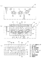
発光素子12の取り付け部分に貫通空間部21を形成する場合には、図4に示したように構成される。なお、図面では、発光素子12や受光素子13,14を表面実装するためのはんだ付け用銅箔であるランド15aを除いて、配線パターンを省略して図示している。以下同じである。
In the case where the through
すなわち、図4(a)に示したように発光素子12の取り付け部分に、平面視方形をなして厚み方向に貫通する穴状の貫通空間部21が形成されている。この貫通空間部21は、発光素子12のチップ12a部分に対応する部分を含んで形成される(図4(b),(c)参照)。
That is, as shown in FIG. 4A, a hole-shaped through
貫通空間21部の形状や大きさは適宜設定されるが、少なくとも前記のように発光素子12のチップ部分12aに対応する部分に形成されていればよい。貫通空間部21の大きさが小さい場合には、特に、チップ12a部分に対応する部位を中心にして貫通空間部21を形成するとよい。
The shape and size of the through
貫通空間部21の大きさや形状は、前記ランド15aを考慮して適宜設定される。
The size and shape of the through
第1受光素子13と第2受光素子14の取り付け部分には、前記のような貫通空間部は形成されない。
The through space portion as described above is not formed in the attachment portion of the first
また、前記ケース16のうち、プリント基板15の下面を覆う下ケース18にも厚み方向に貫通する穴部としての貫通穴22が形成されている。この貫通穴22は、図4(b)、図4(c)に示したように、前記プリント基板15の貫通空間部21に対応する部位に形成される。
Further, in the
図示例では、下ケース18の貫通穴22はプリント基板15の貫通空間部21よりも大きく形成されているが、それと同一又はそれよりも小さく形成されたものであってもよい。
In the illustrated example, the through
なお、図4(b)は、前記発光素子12と2個の受光素子13,14を表面実装して、前記ケース16を取付けたトナー濃度センサ11における上ケース17部分における横断面図である。
4B is a cross-sectional view of the
このように構成されたトナー濃度センサ11では、図4(b)に示したように、発光素子12から照射された照射光は、レンズ部材19方向に向けて進むほか、図4(c)に示したようにプリント基板15方向にも進む。
In the
レンズ部材19方向に進んだ照射光L1はレンズ部材19を透過して前記転写ベルト56で反射し、この反射光L2は再びレンズ部材19を通って前記受光素子13,14で受光される。図4(c)では第1受光素子13のみを図示して第2受光素子14を省略しているが、第2受光素子14の場合も同様である。以下同じである。
Irradiation light L1 traveling in the direction of the
この反射光L2の検知電圧に基づいて前記のようにトナー濃度が検出される。 Based on the detection voltage of the reflected light L2, the toner density is detected as described above.
一方、発光素子12からプリント基板15方向に進んだ光は、プリント基板15の貫通空間部21と下ケース18の貫通穴22を通って外部に放射される。
On the other hand, light traveling from the
照射光の一部はプリント基板15内に進入することもあるが、プリント基板15方向に進む照射光L3の多くが貫通空間部21から放射されるので、プリント基板15内に進入するノイズ光の量を低減できる。ノイズ光が進入しても、僅かであるので、伝播するうちに減衰する。この結果、受光素子13,14に到達するノイズ光は大幅に減る。
Although a part of the irradiation light may enter the printed
したがって、受光素子13,14がノイズ光の影響を受けにくくなり、検出精度の向上を図ることができる。
Therefore, the
しかも、前記貫通空間部21は、発光素子12の取り付け部分に形成されている。つまり、プリント基板15における発光素子12の下を抜いた構造であるので、貫通空間部21を設けるために、別途に面積広さは不要で、面積を有効に活用できる。このため、検出精度が高い小型のトナー濃度センサ11が得られる。
Moreover, the penetrating
また下ケース18にも貫通穴22が形成されているので、発光素子12からの光をより多く外へ放射して、ノイズ光となりうる光を一層減らすことができる。
Further, since the through
このように検出精度の高いトナー濃度センサ11であるので、これを搭載した前記画像形成装置51では、品質の高い画像形成ができる。しかも、トナー濃度センサ11は小型化を測れるので、画像形成装置51内の限られたスペースを有効利用でき、より良い画像成形装置の提供にも貢献できる。
Since the
図5は、前記貫通空間部21の他の例を示している。すなわち、貫通空間部21は全周が囲まれた穴状のものばかりではなく、図5に示したように、プリント基板15の端面まで達する形状、換言すれば端面から切り込んだ形状のものであってもよい。
FIG. 5 shows another example of the through
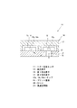
図6は、下ケース18に貫通穴22を形成しない例を示している。このように下ケース18に貫通穴22を形成しない場合には、前記貫通空間部21に対応する部位のプリント基板15側の面18aが、マット(つや消し)状の黒色を呈するようにするのが好ましい。貫通空間部21を通過した照射光L3を吸収して、ノイズ光になりうる光を減らすことができる。
FIG. 6 shows an example in which the through
また、図7に示したように、貫通空間部21に対応する部位のプリント基板15側の面18aにシボ加工部23が形成されたものであってもよい。貫通空間部21を通過した照射光L3を吸収して、ノイズ光になりうる光を減らすことができる。黒色にすること、シボ加工部23を形成することを併用することで、より一層の光の吸収効果が高まる。
In addition, as shown in FIG. 7, a
下ケース18の穴部は、図8に示したように、厚み方向に貫通しない凹みからなる穴部22aであってもよい。この場合も、黒色にしたり、シボ加工部23を形成したりすると、より一層ノイズ光の発生を低減できる。
As shown in FIG. 8, the hole of the
発光素子12の取り付け部分のほかに受光素子13,14の取り付け部分にも貫通空間部21を形成する場合には、図9に示したように構成される。
In the case where the through
すなわち、図9(a)に示したように発光素子12の取り付け部分と第1受光素子13および第2受光素子14の取り付け部分に、平面視方形をなし厚み方向に貫通する穴状の貫通空間部21が形成されている。これらの貫通空間部21は、発光素子12や受光素子13,14のチップ12a,13a,14a部分に対応する部分を含んで形成され、詳細は前述の通りである。
That is, as shown in FIG. 9A, a hole-shaped through space that has a rectangular shape in plan view at the mounting portion of the
また、前記ケース16のうち、プリント基板15の下面を覆う下ケース18にも厚み方向に貫通する穴部としての貫通穴22が形成されている。この貫通穴22は、図9(b)、図9(c)に示したように、前記プリント基板15の発光素子12の下に形成した貫通空間部21に対応する部位のみに形成される。受光素子13,14に下ケース18の外からの光が入り込むのを阻止するためである。
Further, in the
受光素子13,14の下の貫通空間部21に対応する部位に穴部を形成する場合には、図8に示したような厚み方向に貫通しない凹みからなる穴部22a(図8参照)とする。この場合も、黒色にしたり、シボ加工部23(図7参照)を形成したりすると、より一層ノイズ光の発生を低減できる。
When forming a hole in a portion corresponding to the through
このように構成されたトナー濃度センサ11でも、図9(b)に示したように、発光素子12から照射された照射光は、レンズ部材19方向に向けて進むほか、図9(c)に示したようにプリント基板15方向にも進む。
Even in the
レンズ部材19方向に進んだ照射光L1はレンズ部材19を透過して前記転写ベルト56で反射し、この反射光L3は再びレンズ部材19を通って前記受光素子13,14で受光されてトナー濃度が検出されることは、前述と同様である。
Irradiation light L1 traveling in the direction of the
一方の、発光素子12からプリント基板15方向に進んだ照射光L3は、プリント基板15の貫通空間部21と下ケース18の貫通穴22を通って外部に放射される。
On the other hand, the irradiation light L3 traveling from the
照射光の一部はプリント基板15内に進入することもあるが、プリント基板15方向に進む照射光L3の多くが貫通空間部21から放射されるので、プリント基板15内に進入するノイズ光の量を低減できる。ノイズ光が進入しても僅かであるので、伝播するうちに減衰する。その上、受光素子13,14の取り付け部分にも貫通空間部21があるので、この貫通空間部21の内側面において、ノイズ光は拡散して減衰される。前記貫通空間部21は、プレス加工(打ち抜き)やドリル加工によって形成されるが、きれいな切断面は得られず、凹凸が有る形状だからである。このため、受光素子13,14に到達するノイズ光は大幅に減る。
Although a part of the irradiation light may enter the printed
したがって、受光素子13,14がノイズ光の影響を受けにくくなり、検出精度の向上を図ることができる。
Therefore, the
しかも、前記貫通空間部21は、発光素子12の取り付け部分と受光素子13,14の取り付け部分に形成されている。つまり、プリント基板15における発光素子12や受光素子13,14の下を抜いた構造であるので、貫通空間部21を設けるために、別途に面積広さは不要で、面積を有効に活用できる。このため、検出精度が高い小型のトナー濃度センサ11が得られる。
In addition, the through
また下ケース18における発光素子12の下には貫通穴22を有する一方で、受光素子13,14の下には貫通穴22を形成していないので、発光素子12からの光をより多く外へ放射して、ノイズ光となりうる光を一層減らすとともに、受光素子13,14に到達するノイズ光を大幅に減らすことができる。
The
図10は、下ケース18の他の例を示している。すなわち、受光素子13,14の下に形成した貫通空間部21に対応する部位のプリント基板15側の面18aに、シボ加工部23が形成されている。このように構成することによって、受光素子13,14の下の貫通空間部21に進入したノイズ光の再反射を抑えることができる。この結果、受光素子13,14をノイズ光からより良好に保護することができる。
FIG. 10 shows another example of the
図11に示したように、貫通空間部21の内側面にメッキ層24を形成すると、ノイズ光の発生の抑制効果と、ノイズ光の受光素子13,14への到達阻止効果を高めることができる。
As shown in FIG. 11, when the plated
すなわち、図11(a)、図11(c)に示したように、発光素子12と受光素子13,14の下に形成された貫通空間部21の内側面にメッキ層24が形成されている。このメッキ層24は、通常のスルーホールを形成する場合と同じ加工で形成できる。
That is, as shown in FIGS. 11A and 11C, the
このように貫通空間部21の内側面にはメッキ層24があって光を通さないので、発光素子12の下の貫通空間部21では、貫通空間部21からプリント基板15内に入るノイズ光を良好に減らせる。受光素子13,14の下の貫通空間部21では、プリント基板15内を伝播して貫通空間部21に出ようとするノイズ光の透過を阻止する。このため、受光素子13,14に到達するノイズ光を大幅に削減できる。
As described above, since the plated
このようなメッキ層24は、図4などに示したように、発光素子12の下のみに貫通空間部21を形成したときも同様の作用をして、ノイズ光の発生を抑制できる。
As shown in FIG. 4 and the like, such a plated
受光素子13,14の取り付け部分に貫通空間部21を形成する場合には、図12に示したように構成される。
In the case where the through
すなわち、図12(a)に示したように第1受光素子13と第2受光素子14の取り付け部分に、平面視方形をなして厚み方向に貫通する穴状の貫通空間部21が形成されている。これらの貫通空間部21は、受光素子13,14のチップ13a,14a部分に対応する部分を含んで形成され、詳細は前述の通りである。
That is, as shown in FIG. 12A, a hole-shaped through
前記ケース16には、前記のような穴部は形成されない。必要に応じて、貫通空間部21に対応する部位のプリント基板15側の面が、前記のようにマット状の黒色を呈するように形成されたり、シボ加工部23が形成されたりするとよい。
The
このように構成されたトナー濃度センサ11では、図12(b)に示したように、発光素子12から照射された照射光は、レンズ部材19方向に向けて進むほか、図12(c)に示したようにプリント基板15方向にも進む。
In the
レンズ部材19方向に進んだ照射光L1はレンズ部材19を透過して前記転写ベルト56で反射し、この反射光L2は再びレンズ部材19を通って前記受光素子13,14で受光されてトナー濃度が検出されることは、前述と同様である。
Irradiation light L1 traveling in the direction of the
一方、発光素子12からプリント基板15方向に進んだ照射光L3は、プリント基板15内に進入して、プリント基板15と下ケース18との境界面部分で反射したりして、減衰しながらも受光素子13,14側に伝播するが、受光素子13,14の取り付け部分に貫通空間部21があるので、この貫通空間部21の内側面の凹凸において、ノイズ光は拡散して減衰される。このため、受光素子13,14に到達するノイズ光を抑制できる。
On the other hand, the irradiation light L3 traveling from the
したがって、受光素子12がノイズ光の影響を受けにくくなって、検出精度の向上を図ることができる。
Therefore, the
しかも、前記貫通空間部21は、受光素子13,14の取り付け部分に形成されている。つまり、プリント基板15における受光素子13,14の下を抜いた構造であるので、貫通空間部21を設けるために、別途に面積広さは不要で、面積を有効に活用できる。このため、検出精度が高い小型のトナー濃度センサ11が得られる。
Moreover, the penetrating
また下ケース18における受光素子13,14の下の貫通空間部21に対応する部位には穴部を形成していないので、外部からのノイズ光の進入を阻止できる。
Further, since no hole is formed in a portion corresponding to the through
このように、受光素子13,14に到達するノイズ光を大幅に減らすことができる。
Thus, the noise light reaching the
受光素子13,14の取り付け部分にのみ貫通空間部21を形成する場合には、図13に示したように、貫通空間部21の内側面にメッキ層24を形成するとよい。ノイズ光がプリント基板15内から貫通空間部21内に進入するのを阻止できるからである。
When the through
なお、トナー濃度センサ11は、図14に示したように、前記下ケース18がないものもある。その場合には、下ケース18の穴部や色、シボ加工部23による前記のようなノイズ光低減効果を得られないものの、発光素子12または受光素子13,14の少なくともいずれか一方の取り付け部分に形成された貫通空間部21によって、ノイズ光による悪影響を低減することができる。
Note that some
この発明の構成と、前記一形態の構成との対応において、
この発明の発光手段は、前記発光素子12に対応し、
以下同様に、
受光手段は、受光素子(第1受光素子13、第2受光素子14)に対応し、
基板は、プリント基板15に対応し、
穴部は、貫通穴22、穴部22aに対応するも、
この発明は前記構成のみに限定されるものではなく、その他の構成を採用することができる。
In correspondence between the configuration of the present invention and the configuration of the one aspect,
The light emitting means of the present invention corresponds to the
Similarly,
The light receiving means corresponds to the light receiving elements (the first
The board corresponds to the printed
The holes correspond to the through
The present invention is not limited to the above configuration, and other configurations can be adopted.
前記の説明では、トナー濃度センサ11の小型化を図るために、1個の発光素子12と2個の受光素子13,14が略同一直線状に配設されたものを例示したが、例えば「く」の字状などの適宜の配置に配設されたトナー濃度センサであってもよい。前記と同様に、検出精度の向上を図ることができる。
In the above description, in order to reduce the size of the
11…トナー濃度センサ
12…発光素子
13…第1受光素子
14…第2受光素子
12a,13a,14a…チップ
15…プリント基板
16…ケース
18a…貫通空間部に対応する部位の基板側の面
21…貫通空間部
22…貫通穴
22a…穴部
23…シボ加工部
24…メッキ層
51…画像形成装置
DESCRIPTION OF
Claims (8)
前記基板における前記発光手段または受光手段の少なくともいずれか一方の取り付け部分に、厚み方向に貫く貫通空間部が形成された
トナー濃度センサ。 A toner concentration sensor in which a light emitting means for irradiating light to detect toner density and a light receiving means for receiving reflected light emitted from the light emitting means and reflected by a detection target are surface-mounted on a substrate,
A toner concentration sensor in which a through space portion penetrating in a thickness direction is formed in an attachment portion of at least one of the light emitting means and the light receiving means on the substrate.
請求項1に記載のトナー濃度センサ。 The toner density sensor according to claim 1, wherein the penetrating space is formed around a portion corresponding to a chip portion of the light emitting unit or the light receiving unit.
請求項1または請求項2に記載のトナー濃度センサ。 The toner concentration sensor according to claim 1, wherein a plating layer is formed on an inner surface of the through space.
該ケースにおける前記貫通空間部に対応する部位に穴部が形成された
請求項1から請求項3のうちのいずれか一項に記載のトナー濃度センサ。 A case covering the light emitting means and the light receiving means on the substrate;
The toner density sensor according to any one of claims 1 to 3, wherein a hole is formed in a portion of the case corresponding to the through space.
請求項4に記載のトナー濃度センサ。 The toner density sensor according to claim 4, wherein the hole is a through hole penetrating in a thickness direction.
該ケースにおける前記貫通空間部に対応する部位の基板側の面が、マット状の黒色を呈するものである
請求項1から請求項3のうちのいずれか一項に記載のトナー濃度センサ。 A case covering the light emitting means and the light receiving means on the substrate;
4. The toner density sensor according to claim 1, wherein a surface of the portion of the case corresponding to the penetrating space on the substrate side exhibits a matte black color. 5.
該ケースにおける前記貫通空間部に対応する部位の前記基板側の面に、シボ加工部が形成された
請求項1から請求項3のうちのいずれか一項に記載のトナー濃度センサ。 A case covering the light emitting means and the light receiving means on the substrate;
4. The toner density sensor according to claim 1, wherein a textured portion is formed on a surface of the case corresponding to the through space portion on the substrate side. 5.
画像形成装置。 An image forming apparatus equipped with the toner concentration sensor according to claim 1.
Priority Applications (5)
| Application Number | Priority Date | Filing Date | Title |
|---|---|---|---|
| JP2011056991A JP5589914B2 (en) | 2011-03-15 | 2011-03-15 | Toner density sensor and image forming apparatus |
| KR1020120000335A KR101266197B1 (en) | 2011-03-15 | 2012-01-03 | Toner concentration sensor and image formation apparatus |
| US13/347,739 US20120237246A1 (en) | 2011-03-15 | 2012-01-11 | Toner density sensor and image forming apparatus |
| CN201210020890.3A CN102681380B (en) | 2011-03-15 | 2012-01-30 | Toner concentration sensor and image processing system |
| HK12110418.9A HK1169717B (en) | 2011-03-15 | 2012-10-19 | Toner density sensor and image forming apparatus |
Applications Claiming Priority (1)
| Application Number | Priority Date | Filing Date | Title |
|---|---|---|---|
| JP2011056991A JP5589914B2 (en) | 2011-03-15 | 2011-03-15 | Toner density sensor and image forming apparatus |
Publications (2)
| Publication Number | Publication Date |
|---|---|
| JP2012194272A true JP2012194272A (en) | 2012-10-11 |
| JP5589914B2 JP5589914B2 (en) | 2014-09-17 |
Family
ID=46813490
Family Applications (1)
| Application Number | Title | Priority Date | Filing Date |
|---|---|---|---|
| JP2011056991A Active JP5589914B2 (en) | 2011-03-15 | 2011-03-15 | Toner density sensor and image forming apparatus |
Country Status (4)
| Country | Link |
|---|---|
| US (1) | US20120237246A1 (en) |
| JP (1) | JP5589914B2 (en) |
| KR (1) | KR101266197B1 (en) |
| CN (1) | CN102681380B (en) |
Cited By (4)
| Publication number | Priority date | Publication date | Assignee | Title |
|---|---|---|---|---|
| JP2016114363A (en) * | 2014-12-10 | 2016-06-23 | キヤノン株式会社 | Optical device and image forming apparatus including the same |
| JP2017125826A (en) * | 2016-01-15 | 2017-07-20 | オムロン株式会社 | Toner density sensor and image forming apparatus |
| JP2017126043A (en) * | 2016-01-15 | 2017-07-20 | オムロン株式会社 | Toner density sensor and image forming apparatus |
| JP2020140002A (en) * | 2019-02-27 | 2020-09-03 | ブラザー工業株式会社 | Image forming device |
Families Citing this family (9)
| Publication number | Priority date | Publication date | Assignee | Title |
|---|---|---|---|---|
| JP5982875B2 (en) * | 2012-02-29 | 2016-08-31 | 富士ゼロックス株式会社 | Light amount detection apparatus and image forming apparatus |
| US8781353B2 (en) * | 2012-03-30 | 2014-07-15 | Eastman Kodak Company | Toner sensor module |
| US9046851B2 (en) * | 2012-03-30 | 2015-06-02 | Eastman Kodak Company | Method of operating a printer with unfused toner process control |
| JP6369241B2 (en) * | 2014-09-05 | 2018-08-08 | オムロン株式会社 | Reflective sensor |
| JP6477581B2 (en) * | 2016-04-22 | 2019-03-06 | 京セラドキュメントソリューションズ株式会社 | Toner amount detection sensor and image forming apparatus |
| JP6665796B2 (en) * | 2017-01-20 | 2020-03-13 | 京セラドキュメントソリューションズ株式会社 | Integrated sensor and image forming apparatus having the same |
| JP7157555B2 (en) * | 2018-05-24 | 2022-10-20 | キヤノン株式会社 | image forming device |
| JP7327034B2 (en) * | 2019-09-19 | 2023-08-16 | オムロン株式会社 | Toner concentration sensor and image forming apparatus |
| JP7283326B2 (en) * | 2019-09-19 | 2023-05-30 | オムロン株式会社 | Toner concentration sensor and image forming apparatus |
Citations (8)
| Publication number | Priority date | Publication date | Assignee | Title |
|---|---|---|---|---|
| JPS598106U (en) * | 1982-07-08 | 1984-01-19 | ジエコ−株式会社 | Optical sensor mounting structure |
| JPS63197366U (en) * | 1987-06-08 | 1988-12-19 | ||
| JPH04268421A (en) * | 1991-02-22 | 1992-09-24 | Canon Inc | Light amount detection device |
| JPH1062340A (en) * | 1996-08-20 | 1998-03-06 | Sharp Corp | Toner density sensor |
| JP2005024459A (en) * | 2003-07-04 | 2005-01-27 | Ricoh Co Ltd | Optical sensor and image forming apparatus |
| JP2006259447A (en) * | 2005-03-18 | 2006-09-28 | Ricoh Co Ltd | Optical sensor, printed circuit board, and image forming apparatus |
| WO2008105025A1 (en) * | 2007-02-23 | 2008-09-04 | Anywire Corporation | Photoelectric sensor |
| JP2009216662A (en) * | 2008-03-12 | 2009-09-24 | Ricoh Co Ltd | Optical sensor/image forming apparatus |
Family Cites Families (11)
| Publication number | Priority date | Publication date | Assignee | Title |
|---|---|---|---|---|
| US4553033A (en) * | 1983-08-24 | 1985-11-12 | Xerox Corporation | Infrared reflectance densitometer |
| JPH03139673A (en) * | 1989-10-26 | 1991-06-13 | Konica Corp | Destaticizer for copying machine |
| JPH112932A (en) | 1997-06-11 | 1999-01-06 | Fuji Xerox Co Ltd | Density detector and image forming device using the same |
| JP3821639B2 (en) | 2000-08-30 | 2006-09-13 | 康博 小池 | 2-core type light emitting / receiving device for POF communication |
| JP3747279B2 (en) * | 2001-12-13 | 2006-02-22 | シャープ株式会社 | Color image forming apparatus |
| EP1457840B1 (en) * | 2003-03-14 | 2014-07-30 | Ricoh Company, Ltd. | Colour image forming apparatus, which controls the image density by evaluating a reflection signal and a diffuse reflection signal of an optical detecting unit |
| US20040251435A1 (en) * | 2003-04-07 | 2004-12-16 | Noboru Sawayama | Optical sensor and image forming apparatus |
| JP4154272B2 (en) * | 2003-04-07 | 2008-09-24 | 株式会社リコー | Optical sensor and image forming apparatus |
| JP2006267644A (en) * | 2005-03-24 | 2006-10-05 | Canon Inc | Image forming apparatus |
| JP2010014986A (en) * | 2008-07-04 | 2010-01-21 | Konica Minolta Business Technologies Inc | Color image forming apparatus and control method of the same |
| JP2009058520A (en) * | 2008-10-22 | 2009-03-19 | Ricoh Co Ltd | Optical sensor and image forming apparatus |
-
2011
- 2011-03-15 JP JP2011056991A patent/JP5589914B2/en active Active
-
2012
- 2012-01-03 KR KR1020120000335A patent/KR101266197B1/en active Active
- 2012-01-11 US US13/347,739 patent/US20120237246A1/en not_active Abandoned
- 2012-01-30 CN CN201210020890.3A patent/CN102681380B/en active Active
Patent Citations (8)
| Publication number | Priority date | Publication date | Assignee | Title |
|---|---|---|---|---|
| JPS598106U (en) * | 1982-07-08 | 1984-01-19 | ジエコ−株式会社 | Optical sensor mounting structure |
| JPS63197366U (en) * | 1987-06-08 | 1988-12-19 | ||
| JPH04268421A (en) * | 1991-02-22 | 1992-09-24 | Canon Inc | Light amount detection device |
| JPH1062340A (en) * | 1996-08-20 | 1998-03-06 | Sharp Corp | Toner density sensor |
| JP2005024459A (en) * | 2003-07-04 | 2005-01-27 | Ricoh Co Ltd | Optical sensor and image forming apparatus |
| JP2006259447A (en) * | 2005-03-18 | 2006-09-28 | Ricoh Co Ltd | Optical sensor, printed circuit board, and image forming apparatus |
| WO2008105025A1 (en) * | 2007-02-23 | 2008-09-04 | Anywire Corporation | Photoelectric sensor |
| JP2009216662A (en) * | 2008-03-12 | 2009-09-24 | Ricoh Co Ltd | Optical sensor/image forming apparatus |
Cited By (5)
| Publication number | Priority date | Publication date | Assignee | Title |
|---|---|---|---|---|
| JP2016114363A (en) * | 2014-12-10 | 2016-06-23 | キヤノン株式会社 | Optical device and image forming apparatus including the same |
| JP2017125826A (en) * | 2016-01-15 | 2017-07-20 | オムロン株式会社 | Toner density sensor and image forming apparatus |
| JP2017126043A (en) * | 2016-01-15 | 2017-07-20 | オムロン株式会社 | Toner density sensor and image forming apparatus |
| JP2020140002A (en) * | 2019-02-27 | 2020-09-03 | ブラザー工業株式会社 | Image forming device |
| JP7303995B2 (en) | 2019-02-27 | 2023-07-06 | ブラザー工業株式会社 | image forming device |
Also Published As
| Publication number | Publication date |
|---|---|
| US20120237246A1 (en) | 2012-09-20 |
| KR101266197B1 (en) | 2013-05-21 |
| HK1169717A1 (en) | 2013-02-01 |
| CN102681380A (en) | 2012-09-19 |
| JP5589914B2 (en) | 2014-09-17 |
| CN102681380B (en) | 2015-08-19 |
| KR20120105351A (en) | 2012-09-25 |
Similar Documents
| Publication | Publication Date | Title |
|---|---|---|
| JP5589914B2 (en) | Toner density sensor and image forming apparatus | |
| JP2013195066A (en) | Toner density sensor and image forming device | |
| TWI539789B (en) | Image sensor unit, image reading apparatus, and image forming apparatus | |
| JP6004812B2 (en) | Optical detection apparatus and image forming apparatus | |
| JP6566635B2 (en) | Optical device and image forming apparatus including the same | |
| JP6536416B2 (en) | Toner density sensor and image forming apparatus | |
| JP6512115B2 (en) | Toner density sensor and image forming apparatus | |
| US9576229B2 (en) | Image forming apparatus and detection apparatus | |
| JP2006267644A (en) | Image forming apparatus | |
| JP2012053108A (en) | Image forming apparatus and toner concentration detection device | |
| HK1169717B (en) | Toner density sensor and image forming apparatus | |
| JP6896807B2 (en) | Optical device and image forming device equipped with it | |
| JP3740395B2 (en) | Sheet material detecting apparatus, sheet material conveying apparatus, and image forming apparatus | |
| JP2018022017A (en) | Image forming apparatus | |
| JP6477581B2 (en) | Toner amount detection sensor and image forming apparatus | |
| JP2025085920A (en) | Optical Sensors | |
| JP7327034B2 (en) | Toner concentration sensor and image forming apparatus | |
| HK1184537B (en) | Toner density sensor and image forming apparatus | |
| JP2026030778A (en) | Optical Sensor | |
| JP2026074217A (en) | Optical sensor |
Legal Events
| Date | Code | Title | Description |
|---|---|---|---|
| A621 | Written request for application examination |
Free format text: JAPANESE INTERMEDIATE CODE: A621 Effective date: 20130919 |
|
| A977 | Report on retrieval |
Free format text: JAPANESE INTERMEDIATE CODE: A971007 Effective date: 20140226 |
|
| A131 | Notification of reasons for refusal |
Free format text: JAPANESE INTERMEDIATE CODE: A131 Effective date: 20140408 |
|
| A521 | Written amendment |
Free format text: JAPANESE INTERMEDIATE CODE: A523 Effective date: 20140602 |
|
| TRDD | Decision of grant or rejection written | ||
| A01 | Written decision to grant a patent or to grant a registration (utility model) |
Free format text: JAPANESE INTERMEDIATE CODE: A01 Effective date: 20140701 |
|
| A61 | First payment of annual fees (during grant procedure) |
Free format text: JAPANESE INTERMEDIATE CODE: A61 Effective date: 20140714 |
|
| R150 | Certificate of patent or registration of utility model |
Ref document number: 5589914 Country of ref document: JP Free format text: JAPANESE INTERMEDIATE CODE: R150 |