JP2012194599A - Arithmetic unit and error detection method - Google Patents
Arithmetic unit and error detection method Download PDFInfo
- Publication number
- JP2012194599A JP2012194599A JP2011055853A JP2011055853A JP2012194599A JP 2012194599 A JP2012194599 A JP 2012194599A JP 2011055853 A JP2011055853 A JP 2011055853A JP 2011055853 A JP2011055853 A JP 2011055853A JP 2012194599 A JP2012194599 A JP 2012194599A
- Authority
- JP
- Japan
- Prior art keywords
- unit
- nop
- operand
- signal
- arithmetic
- Prior art date
- Legal status (The legal status is an assumption and is not a legal conclusion. Google has not performed a legal analysis and makes no representation as to the accuracy of the status listed.)
- Granted
Links
- 238000001514 detection method Methods 0.000 title claims abstract description 179
- 230000000694 effects Effects 0.000 abstract description 8
- 238000000034 method Methods 0.000 description 15
- 238000010586 diagram Methods 0.000 description 6
- 230000006870 function Effects 0.000 description 6
- 230000005540 biological transmission Effects 0.000 description 5
- 230000004048 modification Effects 0.000 description 3
- 238000012986 modification Methods 0.000 description 3
- 238000005401 electroluminescence Methods 0.000 description 2
- 230000000295 complement effect Effects 0.000 description 1
- 238000003745 diagnosis Methods 0.000 description 1
- 230000002708 enhancing effect Effects 0.000 description 1
- 230000010365 information processing Effects 0.000 description 1
- 238000007689 inspection Methods 0.000 description 1
- 239000004973 liquid crystal related substance Substances 0.000 description 1
- 230000000873 masking effect Effects 0.000 description 1
Images





Landscapes
- Advance Control (AREA)
- Executing Machine-Instructions (AREA)
- Test And Diagnosis Of Digital Computers (AREA)
Abstract
Description
本発明は、演算装置及びエラー検出方法に関する。 The present invention relates to an arithmetic device and an error detection method.
算術演算器のエラーを検出する方法として、一般的には、モジュロ3チェックや、パリティ・プリディクションなどの手法が用いられる。また、この他に、算術演算器全体をエラーの検出対象とする手法が提案されている。
Generally, methods such as
特許文献1は、スーパースカラプロセッサ等で同一の機能を有する2つのALU(Arithmetic Logic Unit)を有する算術論理演算器において、一方のALUにしか有効な演算処理が行われていないタイミングで、両方のALUに同一のデータを与えて同じ処理を実行させ、互いの出力同士を比較することでエラーを検出する方法を開示している。
In
特許文献2は、WAIT状態の時に、機能診断用データが格納された記憶手段からデータを読み出して演算を実行し、演算後の結果を予め格納されていた診断データと比較することでエラーを検出する方法を開示している。
In
パリティ・プリディクション等の一般的なエラー検出方法は、検査回路が複雑な構成になるため、コストや回路規模の都合上、一部の回路にのみ搭載されることが多い。このため、このようなエラー検出方法では、全ての回路におけるエラーを検出することができない。 A general error detection method such as parity prediction has a complicated configuration of an inspection circuit, and is often mounted only on a part of the circuits because of cost and circuit scale. For this reason, such an error detection method cannot detect errors in all circuits.
また、特許文献1が開示する手法は、2つのALUの出力を比較することでエラーを検出する方法であるため、ALUを1つしか有していない算術論理演算器においては適用することができない。
Further, since the method disclosed in
また、特許文献2が開示する手法は、ALUが1つしか有さない場合でも適用できるが、試験データを予め格納しておく必要があり、実行する試験命令や試験データが限られる。よって、エラー検出効果が限定されることとなり、特許文献2が開示する手法では、演算器内でエラーを検出できない箇所が存在し得ることとなる。
The technique disclosed in
本発明は、上記事情に鑑みてなされたものであり、エラーの検出効果を高くすることができる演算装置及びエラー検出方法を提供することを目的とする。 The present invention has been made in view of the above circumstances, and an object of the present invention is to provide an arithmetic device and an error detection method capable of enhancing the error detection effect.
上記目的を達成するため、本発明の第1の観点に係る演算装置は、
演算装置に有効な演算命令が入力されていないNOP状態の検出に従って、受信する入力信号を制御する制御信号を出力するNOP検出部と、
前記NOP検出部が出力した前記制御信号に従って、演算命令を示すOPコード信号を受信し、受信した前記OPコード信号を出力する命令制御部と、
前記NOP検出部が出力した前記制御信号に従って、被演算データを示すオペランド信号を受信し、受信した前記オペランド信号を出力するオペランド制御部と、
前記命令制御部が出力した前記OPコード信号が示す演算命令に従って、前記オペランド制御部が出力した前記オペランド信号が示す被演算データに対する演算処理を実行し、求めた演算結果データを出力する演算部と、
前記演算部が出力した前記演算結果データに基づいて、エラーが発生したか否かを判別するエラー検出部と、を備える、
ことを特徴とする。
In order to achieve the above object, an arithmetic device according to the first aspect of the present invention provides:
A NOP detection unit that outputs a control signal for controlling an input signal to be received in accordance with detection of a NOP state in which a valid operation command is not input to the arithmetic device;
In accordance with the control signal output from the NOP detector, an instruction control unit that receives an OP code signal indicating an operation command and outputs the received OP code signal;
According to the control signal output from the NOP detection unit, an operand control unit that receives an operand signal indicating operation data and outputs the received operand signal;
An arithmetic unit that performs arithmetic processing on the operand data indicated by the operand signal output from the operand control unit according to the arithmetic instruction indicated by the OP code signal output from the instruction control unit, and outputs the obtained arithmetic result data; ,
An error detection unit that determines whether an error has occurred based on the calculation result data output by the calculation unit;
It is characterized by that.
上記目的を達成するため、本発明の第2の観点に係るエラー検出方法は、
演算装置に有効な演算命令が入力されていないNOP状態の検出に従って、受信する入力信号を制御する制御信号を出力するNOP検出ステップと、
前記NOP検出ステップで出力した前記制御信号に従って、演算命令を示すOPコード信号を受信し、受信した前記OPコード信号を出力する命令制御ステップと、
前記NOP検出ステップで出力した前記制御信号に従って、被演算データを示すオペランド信号を受信し、受信した前記オペランド信号を出力するオペランド制御ステップと、
前記命令制御ステップで出力した前記OPコード信号が示す演算命令に従って、前記オペランド制御ステップで出力した前記オペランド信号が示す被演算データに対する演算処理を実行し、求めた演算結果データを出力する演算ステップと、
前記演算ステップで出力した前記演算結果データに基づいて、エラーが発生したか否かを判別するエラー検出ステップと、を備える、
ことを特徴とする。
In order to achieve the above object, an error detection method according to a second aspect of the present invention includes:
A NOP detection step of outputting a control signal for controlling an input signal to be received in accordance with detection of a NOP state in which a valid arithmetic command is not input to the arithmetic device;
In accordance with the control signal output in the NOP detection step, an instruction control step of receiving an OP code signal indicating an operation instruction and outputting the received OP code signal;
According to the control signal output in the NOP detecting step, receiving an operand signal indicating data to be processed, and outputting the received operand signal;
An arithmetic step of performing arithmetic processing on the operand data indicated by the operand signal output in the operand control step and outputting the calculated arithmetic result data in accordance with the arithmetic instruction indicated by the OP code signal output in the instruction control step; ,
An error detection step of determining whether an error has occurred based on the calculation result data output in the calculation step;
It is characterized by that.
本発明によれば、エラーの検出効果を高くすることができる。 According to the present invention, the error detection effect can be enhanced.
本発明の実施形態に係る演算装置について、図面を参照して説明する。 An arithmetic device according to an embodiment of the present invention will be described with reference to the drawings.
[第1実施形態]
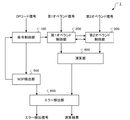
本実施形態に係る演算装置1は、図1に示すように、命令制御部100と、第1オペランド制御部200と、第2オペランド制御部300と、演算部400と、NOP(No Operation)検出部500と、エラー検出部600と、を備える。
[First Embodiment]
As shown in FIG. 1, the
命令制御部100は、演算部400に対する入力信号であるOP(Operation)コード信号を外部から受信し、OPコード信号を演算部400とNOP検出部500に出力する。さらに、命令制御部100は、OPコード信号を再帰的に自身に出力する。
The
なお、OPコード信号とは、演算部400が演算命令を実行する際に必要な全ての制御信号を含む信号である。例えば、有効な演算命令であるか否かを示すバリッド信号や、演算命令の種別を識別する信号、浮動小数点演算である場合の丸め制御信号等である。
The OP code signal is a signal including all control signals necessary when the
第1オペランド制御部200は、入力信号である被演算データとなる第1オペランド信号を外部から受信し、第1オペランド信号を演算部400に出力する。また、第1オペランド制御部200は、第1オペランド信号を第2オペランド制御部300に出力する。
The first
第2オペランド制御部300は、入力信号である被演算データとなる第2オペランド信号を外部から受信し、第2オペランド信号を演算部400に出力する。また、第2オペランド制御部300は、第2オペランド信号を第1オペランド制御部200に出力する。
The second
演算部400は、命令制御部100が出力したOPコード信号と、第1オペランド制御部200と第2オペランド制御部300が出力した第1オペランド信号と第2オペランド信号と、を受信する。演算部400は、OPコード信号が示す演算命令に従って演算処理を行い、演算結果のデータをエラー検出部600に出力する。なお、後述する動作により、演算部400は、タイミングをずらして被演算データを入れ替えて演算処理を実行する。この演算結果のデータも、エラー検出部600に出力される。
The
NOP検出部500は、命令制御部100が出力したOPコード信号を受信し、NOP状態を検出する。NOP検出部500は、NOP検出信号をエラー検出部600に出力し、また、NOP検出信号を命令制御部100、第1オペランド制御部200、第2オペランド制御部300の制御信号として出力する。なお、NOP状態とは、OPコード信号が無効である状態のことである。
The
エラー検出部600は、演算部400が出力した二つの演算結果のデータを比較し、NOP検出部500が出力したNOP検出信号が示す値と、比較結果を示す値とを基に、エラーが発生しているか否かを検出する。また、エラー検出部600は、演算部400が出力した演算結果のデータを、外部に出力する。
The
以上が、演算装置1の構成である。
The above is the configuration of the
続いて、演算装置1の詳細な構成の一例について説明する。
Next, an example of a detailed configuration of the
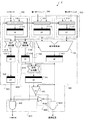
命令制御部100は、図2に示すように、2入力セレクタ110と、OPコードレジスタ120と、から構成される。入力信号であるOPコード信号は、2入力セレクタ110を介してOPコードレジスタ120に記憶される。2入力セレクタ110は、一方の入力を外部からの入力信号であるOPコード信号とし、他方の入力をOPコードレジスタ120から出力されるOPコード信号とする。他方の入力が有効になった場合、OPコードレジスタ120の値が保持されることになる。
The
第1オペランド制御部200は、2入力セレクタ210と、第1オペランドレジスタ220と、から構成される。入力信号である第1オペランド信号は、2入力セレクタ210を介して第1オペランドレジスタ220に記憶される。
The first
第2オペランド制御部300は、2入力セレクタ310と、第2オペランドレジスタ320と、から構成される。入力信号である第2オペランド信号は、2入力セレクタ310を介して第2オペランドレジスタ320に記憶される。
The second
第1オペランドレジスタ220に記憶される第1オペランド信号は、第2オペランド制御部300の2入力セレクタ310に出力される。また、第2オペランドレジスタ320に記憶される第2オペランド信号は、第1オペランド制御部200の2入力セレクタ210に出力される。
The first operand signal stored in the
すなわち、第1オペランド制御部200の2入力セレクタ210は、一方の入力を第1オペランド信号とし、他方の入力を第2オペランド信号とする。また、第2オペランド制御部300の2入力セレクタ310は、一方の入力を第2オペランド信号とし、他方の入力を第1オペランド信号とする。
That is, the two-
演算部400は、算術演算器410と、第1演算結果レジスタ420と、第2演算結果レジスタ430と、から構成される。算術演算器410は、OPコードレジスタ120に記憶されるOPコード信号、第1オペランドレジスタ220と第2オペランドレジスタ320に記憶される二つのオペランド信号、を入力とし、OPコード信号に基づいて演算処理を実行する。第1演算結果レジスタ420は、算術演算器410が出力した演算結果のデータを記憶し、第2演算結果レジスタ430は、第1演算結果レジスタ420が出力した演算結果のデータを記憶する。なお、算術演算器410が実行する演算処理は、加算、乗算、整数加算、整数乗算、浮動小数点加算、浮動小数点乗算等である。
The
NOP検出部500は、NOP検出器510と、第1NOPレジスタ520と、第2NOPレジスタ530と、から構成される。NOP検出器510は、一方の入力を入力信号であるOPコード信号とし、他方の入力をOPコードレジスタ120に記憶されるOPコード信号とする。NOP検出器510が出力するNOP検出信号は、2入力セレクタ110、210、310の制御信号として出力される。第1NOPレジスタ520は、NOP検出器510が出力したNOP検出信号が示す値を記憶する。第2NOPレジスタ530は、第1NOPレジスタ520が出力した値を記憶する。
The
NOP検出器510は、一方の入力、すなわち入力信号であるOPコード信号が無効であり、他方の入力、すなわちOPコードレジスタ120に記憶されているOPコード信号が有効であるタイミングを検出する。すなわち、NOP検出器510は、直前に演算命令が入力されており、かつ、現在演算命令が入力されていないタイミングを検出する。
The
エラー検出部600は、比較器610と、論理積回路620と、から構成される。比較器610は、第1演算結果レジスタ420に記憶された演算結果のデータと、第2演算結果レジスタ430に記憶された演算結果のデータと、を比較する。論理積回路620は、第2NOPレジスタ530に記憶されるNOP検出信号が示す値と比較器610が出力した比較結果を示す値との論理積を出力する。この出力結果が、エラー検出信号となる。
The
以上が、演算装置1の詳細な構成である。
The detailed configuration of the
続いて、演算装置1の具体的な動作の一例について、タイミングチャートを参照して具体的に説明する。
Subsequently, an example of a specific operation of the
図3に示すように、クロックサイクルT1では、有効な演算命令のOPコードMUL(乗算)と、その演算処理に対する第1オペランドY0と、第2オペランドZ0と、が入力されている。 As shown in FIG. 3, in a clock cycle T1, an OP code MUL (multiplication) of a valid operation instruction, a first operand Y0 and a second operand Z0 for the operation processing are input.
クロックサイクルT2では、有効な演算命令のOPコードADD(加算)と、その演算処理に対する第1オペランドY1と、第2オペランドZ1と、が入力されている。また、クロックサイクルT1で入力されたOPコードMULが、OPコードレジスタ120に記憶され、第1オペランドY0が、第1オペランドレジスタ220に記憶され、第2オペランドZ0が、第2オペランドレジスタ320に記憶されている。
In the clock cycle T2, the OP code ADD (addition) of a valid operation instruction, the first operand Y1 for the operation process, and the second operand Z1 are input. The OP code MUL input at clock cycle T1 is stored in the
クロックサイクルT3では、有効な演算命令が存在しないため、NOP検出器510はNOP状態を検出している。また、クロックサイクルT1で入力された演算命令に対する演算処理が終了し、第1演算結果レジスタ420は、演算結果X0を記憶し、演算結果としてX0が出力されている。また、クロックサイクルT2で入力されたOPコードADDが、OPコードレジスタ120に記憶され、第1オペランドY1が、第1オペランドレジスタ220に記憶され、第2オペランドZ1が、第2オペランドレジスタ320に記憶されている。
In clock cycle T3, since there is no valid operation instruction,
クロックサイクルT4では、有効な演算命令のOPコードADDと、その演算処理に対する第1オペランドY2と、第2オペランドZ2と、が入力されている。また、クロックサイクルT2で入力された演算命令に対する演算処理が終了し、第1演算結果レジスタ420は、演算結果X1を記憶し、演算結果としてX1が出力されている。このとき、第2演算結果レジスタ430は、クロックサイクルT1で入力された演算命令の演算結果X0を記憶している。クロックサイクルT4では、有効な演算命令が入力されているため、NOP検出器510はNOP状態を検出しないが、第1NOPレジスタ520は、NOP状態を示す値(例えば真)を記憶している。
In the clock cycle T4, the OP code ADD of a valid operation instruction, the first operand Y2 for the operation processing, and the second operand Z2 are input. Further, the arithmetic processing for the arithmetic instruction input in the clock cycle T2 is completed, the first arithmetic result register 420 stores the arithmetic result X1, and X1 is output as the arithmetic result. At this time, the second operation result register 430 stores the operation result X0 of the operation instruction input in the clock cycle T1. In the clock cycle T4, since a valid operation instruction is input, the
ここで、クロックサイクルT3で出力されたNOP検出信号は、2入力セレクタ110、210、310に出力され、2入力セレクタ110、210、310は、入力信号を切り替える。すなわち、2入力セレクタ110は、OPコードレジスタ120に記憶されているOPコードを入力とし、2入力セレクタ210は、第2オペランドレジスタ320に記憶されている第2オペランドを入力とし、2入力セレクタ310は、第1オペランドレジスタ220に記憶されている第1オペランドを入力とする。
Here, the NOP detection signal output in the clock cycle T3 is output to the 2-
このため、OPコードレジスタ120は、クロックサイクルT3で記憶されたOPコードと同じOPコードADDを記憶し、第1オペランドレジスタ220は、クロックサイクルT3で第2オペランドレジスタ320に記憶された第2オペランドZ1を記憶し、第2オペランドレジスタ320は、クロックサイクルT3で第1オペランドレジスタ220に記憶された第1オペランドY1を記憶する。
Therefore, the OP code register 120 stores the same OP code ADD as the OP code stored in the clock cycle T3, and the
すなわち、クロックサイクルT4では、第1オペランドレジスタ220と第2オペランドレジスタ320に記憶されている値は、NOP状態を検出したクロックサイクルT3で記憶されていた値をそれぞれ入れ替えたデータとなる。
That is, in the clock cycle T4, the values stored in the
なお、クロックサイクルT4では、NOP状態を検出していないため、2入力セレクタ110、210、310の入力は元に戻る。
In the clock cycle T4, since the NOP state is not detected, the inputs of the two-
クロックサイクルT5では、有効な演算命令のOPコードMULと、その演算処理に対する第1オペランドY3と、第2オペランドZ3と、が入力されている。また、OPコードレジスタ120は、クロックサイクルT4で入力されたOPコードADDを記憶し、第1オペランドレジスタ220は、クロックサイクルT4で入力された第1オペランドY2を記憶し、第2オペランドレジスタ320は、クロックサイクルT4で入力された第2オペランドZ2を記憶している。クロックサイクルT4で第1演算結果レジスタ420に記憶された演算結果X1は、第2演算結果レジスタ430に記憶されている。
In the clock cycle T5, the valid operation instruction OP code MUL, the first operand Y3 for the operation processing, and the second operand Z3 are input. The OP code register 120 stores the OP code ADD input in the clock cycle T4, the
また、クロックサイクルT5では、上述のようにクロックサイクルT4で入れ替えたオペランドの演算結果X1’が、第1演算結果レジスタ420に記憶されている。また、クロックサイクルT4で第1NOPレジスタ520に記憶されたNOP検出信号は、クロックサイクルT5では第2NOPレジスタ530に記憶されている。この第2NOPレジスタ530に記憶されているNOP検出信号は、比較器610のイネーブル信号となる。
In the clock cycle T5, the operation result X1 'of the operand replaced in the clock cycle T4 as described above is stored in the first
比較器610は、第1演算結果レジスタ420に記憶されている演算結果X1’と、第2演算結果レジスタ430に記憶されている演算結果X1とを比較し、仮に両値が不一致であった場合、論理積回路620によるイネーブル化を経て、エラー検出信号が出力される。
The
このように、演算装置1は、有効な演算命令が入力されていないタイミングを検出して試験演算命令を実行し、以下の式で表される比較を行い、エラーの検出を行う。
Yn+Zn=Zn+Yn
又は
Yn×Zn=Zn×Yn
なお、Yn、Znは、NOP状態を検出する直前のクロックサイクルにおけるオペランドである。
As described above, the
Yn + Zn = Zn + Yn
Or Yn × Zn = Zn × Yn
Yn and Zn are operands in the clock cycle immediately before the NOP state is detected.
クロックサイクルT6以降は、上述のような動作を実行し、同様にエラーを検出する。 After the clock cycle T6, the above-described operation is performed, and an error is similarly detected.
なお、NOP検出時に入れ替えたデータに対する演算結果は、演算命令に対する出力結果ではないため、演算装置1の外部でこの値を無視する必要がある。また、演算装置1内にこのような値を無視する機構を配置することも可能である。
Note that the operation result for the data exchanged at the time of detecting the NOP is not the output result for the operation instruction, so this value needs to be ignored outside the
以上が、演算装置1の動作の一例である。
The above is an example of the operation of the
以上説明したように、本実施形態に係る演算装置1は、有効な命令がないタイミングを検出して直前の演算命令に対するオペランドを入れ替えて演算処理を実行することで、試験命令や試験データを限定することなくエラーを検出することができる。
As described above, the
また、本実施形態に係る演算装置1は、装置内に算術演算器410が一つしかない場合でも、演算器全体をエラー検出の対象とすることができ、エラー検出効果を高くすることができる。
In addition, the
また、本実施形態に係る演算装置1は、エラーを検出するための回路として、入力信号に対するセレクタ、演算結果を格納するレジスタ、演算結果を比較するための比較器、等を追加する程度であり、いずれも算術演算器410の外部への追加が可能であるため、算術演算器410内部のクリティカルパスに影響を与えない。よって、本実施形態に係る演算装置1は、回路規模や信号遅延等のインパクトを小さくすることができる。
In addition, the
[第2実施形態]
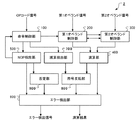
本実施形態に係る演算装置2は、図4に示すように、第1実施形態に係る演算装置1の構成に加え、減算検出部700と、符号反転部800と、否定部900と、を更に備える。演算装置2は、第1実施形態に係る演算装置1が検出できるエラーに加え、整数減算や浮動小数点減算等の演算処理に対してもエラーを検出することができ、さらに試験演算結果のデータをマスクすることができる。なお、第1実施形態に係る演算装置1と同様の機能を実現する要素については、同一の符号を付し、説明を省略する。
[Second Embodiment]
As shown in FIG. 4, the
減算検出部700は、命令制御部100から出力したOPコード信号を受信し、OPコード信号が減算命令であるか否かを検出する。減算検出部700は、減算検出信号を符号反転部800に出力する。
The
符号反転部800は、減算検出部700が出力した減算検出信号と演算部400が出力した演算結果のデータを受信し、受信した減算検出信号が減算を示している場合、すなわち、OPコード信号が減算命令であった場合、演算結果のデータの符号を反転させる。符号反転部800は、符号反転後の演算結果のデータをエラー検出部600に出力する。
The
なお、符号反転とは、整数減算の場合は2の補数を求める処理のことであり、浮動小数点減算の場合は最上位ビットである符号ビットを反転させる処理のことである。 The sign inversion is a process of obtaining a 2's complement in the case of integer subtraction, and a process of inverting the sign bit which is the most significant bit in the case of floating point subtraction.
否定部900は、NOP検出部500が出力したNOP検出信号を否定し、エラー検出部600に出力する。NOP検出信号の否定とは、NOP検出信号が示す値を反転することである。例えば、検出信号が1(真)を示す場合、否定部900は、0(偽)として出力し、検出信号が0(偽)を示す場合、否定部900は、1(真)として出力する。この出力は、試験演算結果の出力をマスクする際に用いられる。
The
以上が、演算装置2の構成である。
The above is the configuration of the
続いて、演算装置2の詳細な構成の一例について説明する。
Next, an example of a detailed configuration of the
減算検出部700は、図5に示すように、減算検出器710と、減算レジスタ720と、から構成される。減算検出器710は、OPコードレジスタ120に記憶されているOPコードを受信し、受信したOPコードが減算命令であるか否かを示す減算検出信号を減算レジスタ720に記憶する。減算レジスタ720に記憶された減算検出信号が示す値は、符号反転器810に出力される。
As shown in FIG. 5, the
符号反転部800は、符号反転器810から構成され、減算レジスタ720に記憶された減算検出信号と第1演算結果レジスタ420に記憶された演算結果のデータを受信する。符号反転器810は、減算レジスタ720に記憶された減算検出信号が減算命令であることを示す値であった場合、受信した演算結果のデータの符号を反転し、符号反転した演算結果のデータを第2演算結果レジスタ430に記憶する。
The
否定部900は、NOTゲート910から構成される。NOTゲート910は、第2NOPレジスタ530に記憶されたNOP検出信号を受信し、受信したNOP検出信号を否定して論理積回路630に出力する。論理積回路630は、NOTゲート910が出力した否定信号と第1演算結果レジスタ420が記憶した演算結果を示すデータを受信し、両値の論理積を出力する。このため、第2NOPレジスタ530にNOPを示す値が記憶されている場合、その値が否定されて論理積が求められるため、試験演算命令の演算結果をマスクすることができる。
The
以上が、演算装置2の詳細な構成の一例である。
The above is an example of the detailed configuration of the
続いて、演算装置2の動作の一例について、タイミングチャートを参照して具体的に説明する。
Next, an example of the operation of the
図6に示すように、クロックサイクルT2では、有効な演算命令であるOPコードSUB(減算)と、その演算処理に対する第1オペランドY1と、第2オペランドZ1と、が入力されている。また、クロックサイクルT3では、有効な演算命令が入力されず、NOP検出器510は、NOPを検出している。このため、第1実施形態と同様に、クロックサイクルT3では、クロックサイクルT2で入力されたオペランドを入れ替えて試験演算命令を実行している。
As shown in FIG. 6, in the clock cycle T2, an OP code SUB (subtraction) that is a valid operation instruction, a first operand Y1 and a second operand Z1 for the operation processing are input. In clock cycle T3, a valid operation instruction is not input, and
クロックサイクルT3では、減算検出器710は、OPコードが減算命令であることを示す減算検出信号を出力し、減算レジスタ720に記憶している。これと同時に、NOP検出器510も、NOP検出信号を出力し、クロックサイクルT4で第1NOPレジスタ520に記憶されている。また、クロックサイクルT4では、第1演算結果レジスタ420に、クロックサイクルT2で入力されたオペランドY1、Z1の減算命令に対する演算結果X1が記憶されている。
In clock cycle T3, the
クロックサイクルT4では、減算レジスタ720にOPコードが減算命令であることを示す値が記憶されているため、符号反転器810は、第1演算結果レジスタ420の出力(X1)に対して符号反転処理を実行する。よって、クロックサイクルT5では、符号反転器810は、符号反転させた演算結果X1を、第2演算結果レジスタ430に記憶する。また、第1演算結果レジスタ420は、クロックサイクルT2で入れ替えられたオペランドに対する演算結果X1’を記憶する。
In clock cycle T4, since the value indicating that the OP code is a subtraction instruction is stored in
クロックサイクルT5では、比較器610は、第1演算結果レジスタ420が記憶している演算結果X1’と、第2演算結果レジスタ430が記憶している符号反転させた演算結果とを比較する。論理積回路620は、比較結果のデータと第2NOPレジスタ530が出力するNOP検出信号との論理積を求め、これをエラー検出信号として出力する。
In the clock cycle T5, the
クロックサイクルT5では、論理積回路630は、第1演算結果レジスタ420が出力するデータと、第2NOPレジスタ530が出力する否定データとの論理積を求める。すなわち、クロックサイクルT5では、第2NOPレジスタ530はNOP状態を示す値を記憶しているため、論理積回路630によって試験演算結果X1’がマスクされる。第2NOPレジスタ530は、演算装置2が試験演算処理を実行するタイミングのみでNOP状態を示す値を記憶している。このため、試験演算結果はマスクされるが、通常の演算結果はマスクされることはない。
In clock cycle T5, the
このように、演算装置2は、第1実施形態と同様に、有効な演算命令が入力されていないタイミングを検出して試験演算命令を実行し、第1実施形態に加え、以下の式で表される比較を行い、エラーの検出を行う。
Yn−Zn=Zn−Yn
なお、Yn、Znは、NOP状態を検出する直前のクロックサイクルにおけるオペランドである。
As described above, as in the first embodiment, the
Yn-Zn = Zn-Yn
Yn and Zn are operands in the clock cycle immediately before the NOP state is detected.
クロックサイクルT6以降も、上述のような動作を実行し、同様にエラーを検出する。 After the clock cycle T6, the above-described operation is performed and an error is detected in the same manner.
以上が、演算装置2の動作の一例である。
The above is an example of the operation of the
以上説明したように、本実施形態に係る演算装置2は、第1実施形態に係る演算装置1が奏する効果に加え、整数減算や浮動小数点減算に対してもエラーを検出することが可能であり、更に、試験演算命令に対する演算結果をマスクすることができる。
As described above, the
演算装置2内で試験演算命令に対する演算結果をマスクすることができるため、外部装置でこのような試験演算命令に対する演算結果を考慮する必要がない。
Since the calculation result for the test calculation command can be masked in the
[第3実施形態]
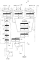
本実施形態に係る演算装置3は、図7に示すように、第1実施形態に係る演算装置1の構成と同様であるが、詳細な構成が異なり、算術演算器410が3Tのパイプライン構造となっている。なお、第1実施形態に係る演算装置1と同様の機能を実現する要素については、同一の符号を付し、説明を省略する。
[Third Embodiment]
As shown in FIG. 7, the
算術演算器410は、内部に第1パイプラインレジスタ440と、第2パイプラインレジスタ450と、を備える。
The
このような構成の場合、NOP検出信号を記憶するレジスタの段数を、パイプラインの段数と合わせれば良い。よって、NOP検出部500は、第3NOPレジスタ540と、第4NOPレジスタ550と、を更に備える。
In such a configuration, the number of register stages storing the NOP detection signal may be matched with the number of pipeline stages. Therefore, the
以上が、演算装置3の詳細な構成の一例である。
The above is an example of the detailed configuration of the
続いて、演算装置3の動作の一例について、タイミングチャートを参照して具体的に説明する。
Next, an example of the operation of the
図8に示すように、クロックサイクルT2では、有効な演算命令であるOPコードADDと、その演算命令に対する第1オペランドY1と、第2オペランドZ1と、が入力される。また、クロックサイクルT3では、有効な命令が存在していない。クロックサイクルT3では、第1オペランドY1と第2オペランドZ1に対する演算処理が実行されるが、算術演算器410がパイプライン構造であるため、演算結果X1は、クロックサイクルT6で第1演算結果レジスタ420に記憶される。その後、演算結果X1は、クロックサイクルT7で第2演算結果レジスタ430に記憶され、オペランドを入れ替えた演算結果X1’との比較が行われる。
As shown in FIG. 8, in a clock cycle T2, an OP code ADD that is a valid operation instruction, a first operand Y1 for the operation instruction, and a second operand Z1 are input. In clock cycle T3, no valid instruction exists. In the clock cycle T3, the arithmetic processing for the first operand Y1 and the second operand Z1 is executed, but since the
クロックサイクルT3では、有効な演算命令が入力されなかったため、NOP検出器510は、NOP検出信号を出力する。これにより、クロックサイクルT4では、第1NOPレジスタ520は、NOPを示す値を記憶する。第2NOPレジスタ530は、クロックサイクルT5にて、第1NOPレジスタが記憶している値を記憶する。第3NOPレジスタ540、第4NOPレジスタ550も同様に、クロックサイクルを1つずつずらしてNOP状態を示す値が記憶される。
In clock cycle T3, since a valid operation instruction has not been input,
NOP状態を示す値を記憶するレジスタを多段構成にすることで、最後の第4NOPレジスタ550は、演算結果を比較するタイミングと同じタイミングでイネーブル信号を出力することができ、エラー検出部600は、エラーを検出することができる。 By making the register for storing the value indicating the NOP state into a multi-stage configuration, the last fourth NOP register 550 can output the enable signal at the same timing as the timing of comparing the operation results. An error can be detected.
このように、演算装置3は、第1実施形態と同様に、算術演算器410がパイプライン構成であっても、有効な演算命令が入力されていないタイミングを検出して試験演算命令を実行することができる。
As described above, similarly to the first embodiment, the
クロックサイクルT6以降も、上述のような動作を実行し、同様にエラーを検出する。 After the clock cycle T6, the above-described operation is performed and an error is detected in the same manner.
以上が、演算装置3の動作の一例である。
The above is an example of the operation of the
以上説明したように、本実施形態に係る演算装置3は、第1実施形態に係る演算装置1が奏する効果に加え、算術演算器410がパイプライン構成であっても、エラーを検出することができる。
As described above, the
[変形例]
本発明は、上記実施形態に限定されず、種々の変形例及び応用が可能である。上記実施形態では、デジタル回路で構成される演算装置について説明したが、これに限られず、コンピュータで構成することも可能である。
[Modification]
The present invention is not limited to the above embodiment, and various modifications and applications are possible. In the above-described embodiment, the arithmetic device including a digital circuit has been described. However, the present invention is not limited to this, and the arithmetic device may be configured with a computer.
この場合、コンピュータで構成される演算装置4は、図9に示すように、制御部11と、主記憶部12と、外部記憶部13と、操作部14と、表示部15と、送受信部16と、から構成される。主記憶部12と、外部記憶部13と、操作部14と、表示部15と、送受信部16とは、いずれも内部バス10を介して制御部11と接続している。
In this case, as shown in FIG. 9, the
送受信部16は、シリアルインタフェースまたはLAN(Local Area Network)インタフェース等から構成されている。送受信部16は、シリアルインタフェースやネットワークを介して送信された情報等を受信する。また、送受信部16は、受信した情報等を、制御部11に供給する。
The transmission /
外部記憶部13は、フラッシュメモリ、ハードディスク、DVD−RAM(Digital Versatile Disc Random−Access Memory)、DVD−RW(Digital Versatile Disc ReWritable)等の不揮発性メモリから構成され、各処理を制御部11に行わせるためのプログラム19を予め記憶し、また、制御部11の指示に従って、外部記憶部13が記憶するデータを制御部11に供給し、制御部11から供給されたデータを記憶する。
The
主記憶部12は、RAM(Random−Access Memory)等から構成され、外部記憶部13に記憶されているプログラム19を読み込み、さらに制御部11の作業領域としても使用される。
The
制御部11は、CPU(Central Processing Unit)等から構成され、外部記憶部13に記憶されているプログラム19に従って、後述する各処理を実行する。
The
操作部14は、キーボードやマウス、操作キーやタッチパネルなどの入力デバイス等と、入力デバイス等を内部バス10に接続するインタフェース装置から構成されている。操作部14は、ユーザの指示を処理する機能を備え、ユーザの操作によって入力されたデータを制御部11に供給する。
The
表示部15は、LCD(Liquid Crystal Display)または有機EL(Electro Luminescence)等から構成されている。表示部15は、各データや情報等を表示する。
The
上述のような一般的な情報処理装置に命令制御部100、第1オペランド制御部200、第2オペランド制御部300、演算部400、NOP検出部500、エラー検出部600、減算検出部700、符号反転部800、否定部900、の各処理を実行させることで、演算装置4は、上述の各実施形態に係る演算装置1〜3と同等の機能、効果を実現することができる。
The general information processing apparatus as described above includes an
なお、本発明は、本発明の広義の趣旨及び範囲を逸脱することなく、様々な実施形態及び変形が可能とされるものである。また、上述した実施形態は、本発明を説明するためのものであり、本発明の範囲を限定するものではない。つまり、本発明の範囲は、実施形態ではなく、特許請求の範囲によって示される。そして、特許請求の範囲内及びそれと同等の発明の意義の範囲内で施される様々な変形が、本発明の範囲内とみなされる。 Note that the present invention can be variously modified and modified without departing from the broad meaning and scope of the present invention. Further, the above-described embodiment is for explaining the present invention, and does not limit the scope of the present invention. That is, the scope of the present invention is shown not by the embodiments but by the claims. Various modifications within the scope of the claims and within the scope of the equivalent invention are considered to be within the scope of the present invention.
上記実施形態の一部又は全ては、以下の付記のようにも記載されうるが、以下には限られない。 A part or all of the above embodiment can be described as in the following supplementary notes, but is not limited thereto.
(付記1)
演算装置に有効な演算命令が入力されていないNOP状態の検出に従って、受信する入力信号を制御する制御信号を出力するNOP検出部と、
前記NOP検出部が出力した前記制御信号に従って、演算命令を示すOPコード信号を受信し、受信した前記OPコード信号を出力する命令制御部と、
前記NOP検出部が出力した前記制御信号に従って、被演算データを示すオペランド信号を受信し、受信した前記オペランド信号を出力するオペランド制御部と、
前記命令制御部が出力した前記OPコード信号が示す演算命令に従って、前記オペランド制御部が出力した前記オペランド信号が示す被演算データに対する演算処理を実行し、求めた演算結果データを出力する演算部と、
前記演算部が出力した前記演算結果データに基づいて、エラーが発生したか否かを判別するエラー検出部と、を備える、
ことを特徴とする演算装置。
(Appendix 1)
A NOP detection unit that outputs a control signal for controlling an input signal to be received in accordance with detection of a NOP state in which a valid operation command is not input to the arithmetic device;
In accordance with the control signal output from the NOP detector, an instruction control unit that receives an OP code signal indicating an operation command and outputs the received OP code signal;
According to the control signal output from the NOP detection unit, an operand control unit that receives an operand signal indicating operation data and outputs the received operand signal;
An arithmetic unit that performs arithmetic processing on the operand data indicated by the operand signal output from the operand control unit according to the arithmetic instruction indicated by the OP code signal output from the instruction control unit, and outputs the obtained arithmetic result data; ,
An error detection unit that determines whether an error has occurred based on the calculation result data output by the calculation unit;
An arithmetic device characterized by that.
(付記2)
前記命令制御部は、前記NOP検出部が前記NOP状態を検出した場合、直前に受信した前記OPコード信号を前記演算部に出力し、
前記オペランド制御部は、前記NOP検出部が前記NOP状態を検出した場合、直前に受信した前記オペランド信号を前記演算部に出力し、
前記エラー検出部は、前記演算部が直前に求めた前記演算結果データと前記NOP状態を検出した際に求めた前記演算結果データとを比較し、それぞれが異なる場合にエラーが発生したと判断する、
ことを特徴とする付記1に記載の演算装置。
(Appendix 2)
When the NOP detection unit detects the NOP state, the command control unit outputs the OP code signal received immediately before to the arithmetic unit,
When the NOP detection unit detects the NOP state, the operand control unit outputs the operand signal received immediately before to the arithmetic unit,
The error detection unit compares the calculation result data obtained immediately before by the calculation unit with the calculation result data obtained when the NOP state is detected, and determines that an error has occurred when they are different from each other. ,
The arithmetic unit according to
(付記3)
前記オペランド制御部は、第1オペランド制御部と、第2オペランド制御部と、を備え、
前記第1オペランド制御部は、
前記NOP検出部が前記NOP状態を検出していない場合、第1オペランド信号を受信し、受信した前記第1オペランド信号を前記演算部に出力し、
前記NOP検出部が前記NOP状態を検出した場合、直前に受信した前記第1オペランド信号を前記第2オペランド制御部に出力し、前記第2オペランド制御部が出力した第2オペランド信号を受信し、受信した前記第2オペランド信号を前記演算部に出力し、
前記第2オペランド制御部は、
前記NOP検出部が前記NOP状態を検出していない場合、前記第2オペランド信号を受信し、受信した前記第2オペランド信号を前記演算部に出力し、
前記NOP検出部が前記NOP状態を検出した場合、直前に受信した前記第2オペランド信号を前記第1オペランド制御部に出力し、前記第1オペランド制御部が出力した前記第1オペランド信号を受信し、受信した前記第1オペランド信号を前記演算部に出力する、
ことを特徴とする付記1又は2に記載の演算装置。
(Appendix 3)
The operand control unit includes a first operand control unit and a second operand control unit,
The first operand controller is
When the NOP detection unit does not detect the NOP state, the first operand signal is received, and the received first operand signal is output to the arithmetic unit,
When the NOP detection unit detects the NOP state, the first operand signal received immediately before is output to the second operand control unit, and the second operand signal output by the second operand control unit is received. Outputting the received second operand signal to the arithmetic unit;
The second operand controller is
When the NOP detection unit does not detect the NOP state, the second operand signal is received, and the received second operand signal is output to the arithmetic unit,
When the NOP detection unit detects the NOP state, the second operand signal received immediately before is output to the first operand control unit, and the first operand signal output by the first operand control unit is received. Outputting the received first operand signal to the arithmetic unit;
The arithmetic unit according to
(付記4)
前記NOP検出部は、前記NOP状態を検出したことを示すNOP検出信号を前記エラー検出部に出力し、
前記エラー検出部は、前記NOP検出信号を受信し、前記NOP検出信号が前記NOP状態を示している場合、かつ、エラーが発生したと判別した場合、エラーが発生したことを示すエラー検出信号を出力する、
ことを特徴とする付記1乃至3のいずれか1つに記載の演算装置。
(Appendix 4)
The NOP detection unit outputs a NOP detection signal indicating that the NOP state has been detected to the error detection unit,
The error detection unit receives the NOP detection signal, and when the NOP detection signal indicates the NOP state and determines that an error has occurred, an error detection signal indicating that an error has occurred. Output,
The arithmetic unit according to any one of
(付記5)
前記OPコード信号が減算命令を示しているか否かを検出する減算検出部と、
前記演算部が求めた前記演算結果データの符号を反転させる符号反転部と、を更に備え、
前記符号反転部は、前記減算検出部が前記減算命令を検出した場合、前記演算部が求めた前記演算結果データの符号を反転し、
前記エラー検出部は、前記演算部が求めた前記演算結果データと、前記符号反転部が符号を反転した前記演算結果データとを比較する、
ことを特徴とする付記1乃至4のいずれか1つに記載の演算装置。
(Appendix 5)
A subtraction detector that detects whether the OP code signal indicates a subtraction instruction;
A code inversion unit for inverting the sign of the calculation result data obtained by the calculation unit,
When the subtraction detection unit detects the subtraction instruction, the sign inversion unit inverts the sign of the operation result data obtained by the operation unit,
The error detection unit compares the calculation result data obtained by the calculation unit with the calculation result data obtained by inverting the sign of the sign inverting unit.
The arithmetic unit according to any one of
(付記6)
前記NOP検出部が出力した前記NOP検出信号を否定する否定部をさらに備え、
前記否定部は、否定した前記NOP検出信号を前記エラー検出部に出力し、
前記エラー検出部は、前記演算部が求めた前記演算結果データと前記否定部が否定して出力した前記NOP検出信号が示す値との論理積を求め、求めた前記論理積を前記演算結果データとして出力する、
ことを特徴とする付記1乃至5のいずれか1つに記載に演算装置。
(Appendix 6)
A negative unit that negates the NOP detection signal output by the NOP detection unit;
The negative part outputs the negative NOP detection signal to the error detection part,
The error detection unit obtains a logical product of the computation result data obtained by the computation unit and a value indicated by the NOP detection signal output by negation by the negation unit, and obtains the obtained logical product as the computation result data. Output as
The arithmetic unit according to any one of
(付記7)
前記演算部は、パイプライン構成であり、
前記NOP検出部は、前記NOP検出信号が示す値を記憶する記憶部を前記パイプラインの段数に従った数備える、
ことを特徴とする付記1乃至6のいずれか1つに記載の演算装置。
(Appendix 7)
The arithmetic unit has a pipeline configuration,
The NOP detection unit includes a number of storage units that store a value indicated by the NOP detection signal according to the number of stages of the pipeline.
The arithmetic unit according to any one of
(付記8)
前記命令制御部は、受信した前記OPコード信号を記憶するOPコード記憶部を備え、
前記第1オペランド制御部は、受信した前記オペランド信号を記憶する第1オペランド記憶部を備え、
前記第2オペランド制御部は、受信した前記オペランド信号を記憶する第2オペランド記憶部を備え、
前記NOP検出部は、前記NOP検出信号を記憶する第1NOP記憶部と、前記第1NOP記憶部が記憶している前記NOP検出信号を記憶する第2NOP記憶部と、を備え、
前記演算部は、前記演算結果データを記憶する第1演算結果記憶部と、前記第1演算結果記憶部が記憶している前記演算結果データを記憶する第2演算結果記憶部と、を備え、
前記NOP検出部が前記NOP状態を検出した第1のクロックサイクルにおいて、
前記NOP検出部は、前記第1NOP記憶部に前記NOP検出信号を記憶し、前記制御信号を前記命令制御部と前記第1オペランド制御部及び前記第2オペランド制御部に出力し、
前記命令制御部は、直前に受信した前記OPコード信号を前記OPコード記憶部に記憶し、前記OPコード記憶部に記憶された前記OPコード信号を前記演算部に出力し、
前記第1オペランド制御部は、前記第2オペランド制御部から受信した前記第2オペランド信号を前記第1オペランド記憶部に記憶し、前記第1オペランド記憶部に記憶された前記第2オペランド信号を前記演算部に出力し、
前記第2オペランド制御部は、前記第1オペランド制御部から受信した前記第1オペランド信号を前記第2オペランド記憶部に記憶し、前記第2オペランド記憶部に記憶された前記第1オペランド信号を前記演算部に出力し、
前記演算部は、求めた前記演算結果データを前記第1演算結果記憶部に記憶する、
ことを特徴とする付記3に記載の演算装置。
(Appendix 8)
The command control unit includes an OP code storage unit that stores the received OP code signal.
The first operand control unit includes a first operand storage unit that stores the received operand signal,
The second operand control unit includes a second operand storage unit that stores the received operand signal.
The NOP detection unit includes a first NOP storage unit that stores the NOP detection signal, and a second NOP storage unit that stores the NOP detection signal stored in the first NOP storage unit,
The calculation unit includes a first calculation result storage unit that stores the calculation result data, and a second calculation result storage unit that stores the calculation result data stored in the first calculation result storage unit,
In the first clock cycle in which the NOP detector detects the NOP state,
The NOP detection unit stores the NOP detection signal in the first NOP storage unit, and outputs the control signal to the instruction control unit, the first operand control unit, and the second operand control unit,
The instruction control unit stores the OP code signal received immediately before in the OP code storage unit, and outputs the OP code signal stored in the OP code storage unit to the arithmetic unit,
The first operand control unit stores the second operand signal received from the second operand control unit in the first operand storage unit, and stores the second operand signal stored in the first operand storage unit. Output to the arithmetic unit,
The second operand control unit stores the first operand signal received from the first operand control unit in the second operand storage unit, and stores the first operand signal stored in the second operand storage unit. Output to the arithmetic unit,
The calculation unit stores the calculated calculation result data in the first calculation result storage unit.
The arithmetic unit according to
(付記9)
前記第1のクロックサイクルの次の第2のクロックサイクルにおいて、
前記NOP検出部は、前記第1NOP記憶部に記憶された前記NOP検出信号を前記第2NOP記憶部に記憶し、前記第2NOP記憶部に記憶された前記NOP検出信号を前記エラー検出部に出力し、
前記演算部は、前記第1演算結果記憶部に記憶された前記演算結果データを前記第2演算結果記憶部に記憶し、前記命令制御部と前記第1オペランド制御部及び前記第2オペランド制御部の出力信号に従って試験演算結果データを求め、求めた前記試験演算結果データを前記第1演算結果記憶部に記憶し、前記第1演算結果記憶部に記憶された前記試験演算結果データと前記第2演算結果記憶部に記憶された前記演算結果データを前記エラー検出部に出力し、
前記エラー検出部は、前記演算部が出力した前記試験演算結果データと前記演算結果データとを比較し、両者が異なる値である場合、かつ、前記NOP検出部が出力した前記NOP検出信号が前記NOP状態を示している場合、前記エラー検出信号を出力する、
ことを特徴とする付記8に記載の演算装置。
(Appendix 9)
In a second clock cycle following the first clock cycle,
The NOP detection unit stores the NOP detection signal stored in the first NOP storage unit in the second NOP storage unit, and outputs the NOP detection signal stored in the second NOP storage unit to the error detection unit. ,
The calculation unit stores the calculation result data stored in the first calculation result storage unit in the second calculation result storage unit, and the instruction control unit, the first operand control unit, and the second operand control unit. The test calculation result data is obtained in accordance with the output signal, the obtained test calculation result data is stored in the first calculation result storage unit, and the test calculation result data stored in the first calculation result storage unit and the second calculation result storage unit are stored. The calculation result data stored in the calculation result storage unit is output to the error detection unit,
The error detection unit compares the test calculation result data output from the calculation unit with the calculation result data, and when both are different values, the NOP detection signal output from the NOP detection unit is When the NOP state is indicated, the error detection signal is output.
The arithmetic unit according to appendix 8, characterized by:
(付記10)
演算装置に有効な演算命令が入力されていないNOP状態の検出に従って、受信する入力信号を制御する制御信号を出力するNOP検出ステップと、
前記NOP検出ステップで出力した前記制御信号に従って、演算命令を示すOPコード信号を受信し、受信した前記OPコード信号を出力する命令制御ステップと、
前記NOP検出ステップで出力した前記制御信号に従って、被演算データを示すオペランド信号を受信し、受信した前記オペランド信号を出力するオペランド制御ステップと、
前記命令制御ステップで出力した前記OPコード信号が示す演算命令に従って、前記オペランド制御ステップで出力した前記オペランド信号が示す被演算データに対する演算処理を実行し、求めた演算結果データを出力する演算ステップと、
前記演算ステップで出力した前記演算結果データに基づいて、エラーが発生したか否かを判別するエラー検出ステップと、を備える、
ことを特徴とするエラー検出方法。
(Appendix 10)
A NOP detection step of outputting a control signal for controlling an input signal to be received in accordance with detection of a NOP state in which a valid arithmetic command is not input to the arithmetic device;
In accordance with the control signal output in the NOP detection step, an instruction control step of receiving an OP code signal indicating an operation instruction and outputting the received OP code signal;
According to the control signal output in the NOP detecting step, receiving an operand signal indicating data to be processed, and outputting the received operand signal;
An arithmetic step of performing arithmetic processing on the operand data indicated by the operand signal output in the operand control step and outputting the calculated arithmetic result data in accordance with the arithmetic instruction indicated by the OP code signal output in the instruction control step; ,
An error detection step of determining whether an error has occurred based on the calculation result data output in the calculation step;
An error detection method characterized by the above.
1、2、3、4 演算装置
100 命令制御部
200 第1オペランド制御部
300 第2オペランド制御部
400 演算部
500 NOP検出部
600 エラー検出部
700 減算検出部
800 符号反転部
900 否定部
110、210、310 2入力セレクタ
120 OPコードレジスタ
220 第1オペランドレジスタ
320 第2オペランドレジスタ
410 算術演算器
420 第1演算結果レジスタ
430 第2演算結果レジスタ
440 第1パイプラインレジスタ
450 第2パイプラインレジスタ
510 NOP検出器
520 第1NOPレジスタ
530 第2NOPレジスタ
540 第3NOPレジスタ
550 第4NOPレジスタ
610 比較器
620、630 論理積回路
710 減算検出器
720 減算レジスタ
810 符号反転器
910 NOTゲート
10 内部バス
11 制御部
12 主記憶部
13 外部記憶部
14 操作部
15 表示部
16 送受信部
19 プログラム
1, 2, 3, 4
Claims (10)
前記NOP検出部が出力した前記制御信号に従って、演算命令を示すOPコード信号を受信し、受信した前記OPコード信号を出力する命令制御部と、
前記NOP検出部が出力した前記制御信号に従って、被演算データを示すオペランド信号を受信し、受信した前記オペランド信号を出力するオペランド制御部と、
前記命令制御部が出力した前記OPコード信号が示す演算命令に従って、前記オペランド制御部が出力した前記オペランド信号が示す被演算データに対する演算処理を実行し、求めた演算結果データを出力する演算部と、
前記演算部が出力した前記演算結果データに基づいて、エラーが発生したか否かを判別するエラー検出部と、を備える、
ことを特徴とする演算装置。 A NOP detection unit that outputs a control signal for controlling an input signal to be received in accordance with detection of a NOP state in which a valid operation command is not input to the arithmetic device;
In accordance with the control signal output from the NOP detector, an instruction control unit that receives an OP code signal indicating an operation command and outputs the received OP code signal;
According to the control signal output from the NOP detection unit, an operand control unit that receives an operand signal indicating operation data and outputs the received operand signal;
An arithmetic unit that performs arithmetic processing on the operand data indicated by the operand signal output from the operand control unit according to the arithmetic instruction indicated by the OP code signal output from the instruction control unit, and outputs the obtained arithmetic result data; ,
An error detection unit that determines whether an error has occurred based on the calculation result data output by the calculation unit;
An arithmetic device characterized by that.
前記オペランド制御部は、前記NOP検出部が前記NOP状態を検出した場合、直前に受信した前記オペランド信号を前記演算部に出力し、
前記エラー検出部は、前記演算部が直前に求めた前記演算結果データと前記NOP状態を検出した際に求めた前記演算結果データとを比較し、それぞれが異なる場合にエラーが発生したと判断する、
ことを特徴とする請求項1に記載の演算装置。 When the NOP detection unit detects the NOP state, the command control unit outputs the OP code signal received immediately before to the arithmetic unit,
When the NOP detection unit detects the NOP state, the operand control unit outputs the operand signal received immediately before to the arithmetic unit,
The error detection unit compares the calculation result data obtained immediately before by the calculation unit with the calculation result data obtained when the NOP state is detected, and determines that an error has occurred when they are different from each other. ,
The arithmetic unit according to claim 1.
前記第1オペランド制御部は、
前記NOP検出部が前記NOP状態を検出していない場合、第1オペランド信号を受信し、受信した前記第1オペランド信号を前記演算部に出力し、
前記NOP検出部が前記NOP状態を検出した場合、直前に受信した前記第1オペランド信号を前記第2オペランド制御部に出力し、前記第2オペランド制御部が出力した第2オペランド信号を受信し、受信した前記第2オペランド信号を前記演算部に出力し、
前記第2オペランド制御部は、
前記NOP検出部が前記NOP状態を検出していない場合、前記第2オペランド信号を受信し、受信した前記第2オペランド信号を前記演算部に出力し、
前記NOP検出部が前記NOP状態を検出した場合、直前に受信した前記第2オペランド信号を前記第1オペランド制御部に出力し、前記第1オペランド制御部が出力した前記第1オペランド信号を受信し、受信した前記第1オペランド信号を前記演算部に出力する、
ことを特徴とする請求項1又は2に記載の演算装置。 The operand control unit includes a first operand control unit and a second operand control unit,
The first operand controller is
When the NOP detection unit does not detect the NOP state, the first operand signal is received, and the received first operand signal is output to the arithmetic unit,
When the NOP detection unit detects the NOP state, the first operand signal received immediately before is output to the second operand control unit, and the second operand signal output by the second operand control unit is received. Outputting the received second operand signal to the arithmetic unit;
The second operand controller is
When the NOP detection unit does not detect the NOP state, the second operand signal is received, and the received second operand signal is output to the arithmetic unit,
When the NOP detection unit detects the NOP state, the second operand signal received immediately before is output to the first operand control unit, and the first operand signal output by the first operand control unit is received. Outputting the received first operand signal to the arithmetic unit;
The arithmetic unit according to claim 1 or 2, wherein
前記エラー検出部は、前記NOP検出信号を受信し、前記NOP検出信号が前記NOP状態を示している場合、かつ、エラーが発生したと判別した場合、エラーが発生したことを示すエラー検出信号を出力する、
ことを特徴とする請求項1乃至3のいずれか1項に記載の演算装置。 The NOP detection unit outputs a NOP detection signal indicating that the NOP state has been detected to the error detection unit,
The error detection unit receives the NOP detection signal, and when the NOP detection signal indicates the NOP state and determines that an error has occurred, an error detection signal indicating that an error has occurred. Output,
The arithmetic unit according to any one of claims 1 to 3, wherein
前記演算部が求めた前記演算結果データの符号を反転させる符号反転部と、を更に備え、
前記符号反転部は、前記減算検出部が前記減算命令を検出した場合、前記演算部が求めた前記演算結果データの符号を反転し、
前記エラー検出部は、前記演算部が求めた前記演算結果データと、前記符号反転部が符号を反転した前記演算結果データとを比較する、
ことを特徴とする請求項1乃至4のいずれか1項に記載の演算装置。 A subtraction detector that detects whether the OP code signal indicates a subtraction instruction;
A code inversion unit for inverting the sign of the calculation result data obtained by the calculation unit,
When the subtraction detection unit detects the subtraction instruction, the sign inversion unit inverts the sign of the operation result data obtained by the operation unit,
The error detection unit compares the calculation result data obtained by the calculation unit with the calculation result data obtained by inverting the sign of the sign inverting unit.
The arithmetic unit according to claim 1, wherein the arithmetic unit is any one of the above.
前記否定部は、否定した前記NOP検出信号を前記エラー検出部に出力し、
前記エラー検出部は、前記演算部が求めた前記演算結果データと前記否定部が否定して出力した前記NOP検出信号が示す値との論理積を求め、求めた前記論理積を前記演算結果データとして出力する、
ことを特徴とする請求項1乃至5のいずれか1項に記載に演算装置。 A negative unit that negates the NOP detection signal output by the NOP detection unit;
The negative part outputs the negative NOP detection signal to the error detection part,
The error detection unit obtains a logical product of the computation result data obtained by the computation unit and a value indicated by the NOP detection signal output by negation by the negation unit, and obtains the obtained logical product as the computation result data. Output as
The arithmetic unit according to any one of claims 1 to 5, wherein:
前記NOP検出部は、前記NOP検出信号が示す値を記憶する記憶部を前記パイプラインの段数に従った数備える、
ことを特徴とする請求項1乃至6のいずれか1項に記載の演算装置。 The arithmetic unit has a pipeline configuration,
The NOP detection unit includes a number of storage units that store a value indicated by the NOP detection signal according to the number of stages of the pipeline.
The arithmetic unit according to claim 1, wherein
前記第1オペランド制御部は、受信した前記オペランド信号を記憶する第1オペランド記憶部を備え、
前記第2オペランド制御部は、受信した前記オペランド信号を記憶する第2オペランド記憶部を備え、
前記NOP検出部は、前記NOP検出信号を記憶する第1NOP記憶部と、前記第1NOP記憶部が記憶している前記NOP検出信号を記憶する第2NOP記憶部と、を備え、
前記演算部は、前記演算結果データを記憶する第1演算結果記憶部と、前記第1演算結果記憶部が記憶している前記演算結果データを記憶する第2演算結果記憶部と、を備え、
前記NOP検出部が前記NOP状態を検出した第1のクロックサイクルにおいて、
前記NOP検出部は、前記第1NOP記憶部に前記NOP検出信号を記憶し、前記制御信号を前記命令制御部と前記第1オペランド制御部及び前記第2オペランド制御部に出力し、
前記命令制御部は、直前に受信した前記OPコード信号を前記OPコード記憶部に記憶し、前記OPコード記憶部に記憶された前記OPコード信号を前記演算部に出力し、
前記第1オペランド制御部は、前記第2オペランド制御部から受信した前記第2オペランド信号を前記第1オペランド記憶部に記憶し、前記第1オペランド記憶部に記憶された前記第2オペランド信号を前記演算部に出力し、
前記第2オペランド制御部は、前記第1オペランド制御部から受信した前記第1オペランド信号を前記第2オペランド記憶部に記憶し、前記第2オペランド記憶部に記憶された前記第1オペランド信号を前記演算部に出力し、
前記演算部は、求めた前記演算結果データを前記第1演算結果記憶部に記憶する、
ことを特徴とする請求項3に記載の演算装置。 The command control unit includes an OP code storage unit that stores the received OP code signal.
The first operand control unit includes a first operand storage unit that stores the received operand signal,
The second operand control unit includes a second operand storage unit that stores the received operand signal.
The NOP detection unit includes a first NOP storage unit that stores the NOP detection signal, and a second NOP storage unit that stores the NOP detection signal stored in the first NOP storage unit,
The calculation unit includes a first calculation result storage unit that stores the calculation result data, and a second calculation result storage unit that stores the calculation result data stored in the first calculation result storage unit,
In the first clock cycle in which the NOP detector detects the NOP state,
The NOP detection unit stores the NOP detection signal in the first NOP storage unit, and outputs the control signal to the instruction control unit, the first operand control unit, and the second operand control unit,
The instruction control unit stores the OP code signal received immediately before in the OP code storage unit, and outputs the OP code signal stored in the OP code storage unit to the arithmetic unit,
The first operand control unit stores the second operand signal received from the second operand control unit in the first operand storage unit, and stores the second operand signal stored in the first operand storage unit. Output to the arithmetic unit,
The second operand control unit stores the first operand signal received from the first operand control unit in the second operand storage unit, and stores the first operand signal stored in the second operand storage unit. Output to the arithmetic unit,
The calculation unit stores the calculated calculation result data in the first calculation result storage unit.
The arithmetic unit according to claim 3.
前記NOP検出部は、前記第1NOP記憶部に記憶された前記NOP検出信号を前記第2NOP記憶部に記憶し、前記第2NOP記憶部に記憶された前記NOP検出信号を前記エラー検出部に出力し、
前記演算部は、前記第1演算結果記憶部に記憶された前記演算結果データを前記第2演算結果記憶部に記憶し、前記命令制御部と前記第1オペランド制御部及び前記第2オペランド制御部の出力信号に従って試験演算結果データを求め、求めた前記試験演算結果データを前記第1演算結果記憶部に記憶し、前記第1演算結果記憶部に記憶された前記試験演算結果データと前記第2演算結果記憶部に記憶された前記演算結果データを前記エラー検出部に出力し、
前記エラー検出部は、前記演算部が出力した前記試験演算結果データと前記演算結果データとを比較し、両者が異なる値である場合、かつ、前記NOP検出部が出力した前記NOP検出信号が前記NOP状態を示している場合、前記エラー検出信号を出力する、
ことを特徴とする請求項8に記載の演算装置。 In a second clock cycle following the first clock cycle,
The NOP detection unit stores the NOP detection signal stored in the first NOP storage unit in the second NOP storage unit, and outputs the NOP detection signal stored in the second NOP storage unit to the error detection unit. ,
The calculation unit stores the calculation result data stored in the first calculation result storage unit in the second calculation result storage unit, and the instruction control unit, the first operand control unit, and the second operand control unit. The test calculation result data is obtained in accordance with the output signal, the obtained test calculation result data is stored in the first calculation result storage unit, and the test calculation result data stored in the first calculation result storage unit and the second calculation result storage unit are stored. The calculation result data stored in the calculation result storage unit is output to the error detection unit,
The error detection unit compares the test calculation result data output from the calculation unit with the calculation result data, and when both are different values, the NOP detection signal output from the NOP detection unit is When the NOP state is indicated, the error detection signal is output.
The arithmetic unit according to claim 8.
前記NOP検出ステップで出力した前記制御信号に従って、演算命令を示すOPコード信号を受信し、受信した前記OPコード信号を出力する命令制御ステップと、
前記NOP検出ステップで出力した前記制御信号に従って、被演算データを示すオペランド信号を受信し、受信した前記オペランド信号を出力するオペランド制御ステップと、
前記命令制御ステップで出力した前記OPコード信号が示す演算命令に従って、前記オペランド制御ステップで出力した前記オペランド信号が示す被演算データに対する演算処理を実行し、求めた演算結果データを出力する演算ステップと、
前記演算ステップで出力した前記演算結果データに基づいて、エラーが発生したか否かを判別するエラー検出ステップと、を備える、
ことを特徴とするエラー検出方法。 A NOP detection step of outputting a control signal for controlling an input signal to be received in accordance with detection of a NOP state in which a valid arithmetic command is not input to the arithmetic device;
In accordance with the control signal output in the NOP detection step, an instruction control step of receiving an OP code signal indicating an operation instruction and outputting the received OP code signal;
According to the control signal output in the NOP detecting step, receiving an operand signal indicating data to be processed, and outputting the received operand signal;
An arithmetic step of performing arithmetic processing on the operand data indicated by the operand signal output in the operand control step and outputting the calculated arithmetic result data in accordance with the arithmetic instruction indicated by the OP code signal output in the instruction control step; ,
An error detection step of determining whether an error has occurred based on the calculation result data output in the calculation step;
An error detection method characterized by the above.
Priority Applications (1)
| Application Number | Priority Date | Filing Date | Title |
|---|---|---|---|
| JP2011055853A JP5732933B2 (en) | 2011-03-14 | 2011-03-14 | Arithmetic apparatus and error detection method |
Applications Claiming Priority (1)
| Application Number | Priority Date | Filing Date | Title |
|---|---|---|---|
| JP2011055853A JP5732933B2 (en) | 2011-03-14 | 2011-03-14 | Arithmetic apparatus and error detection method |
Publications (2)
| Publication Number | Publication Date |
|---|---|
| JP2012194599A true JP2012194599A (en) | 2012-10-11 |
| JP5732933B2 JP5732933B2 (en) | 2015-06-10 |
Family
ID=47086477
Family Applications (1)
| Application Number | Title | Priority Date | Filing Date |
|---|---|---|---|
| JP2011055853A Expired - Fee Related JP5732933B2 (en) | 2011-03-14 | 2011-03-14 | Arithmetic apparatus and error detection method |
Country Status (1)
| Country | Link |
|---|---|
| JP (1) | JP5732933B2 (en) |
Citations (5)
| Publication number | Priority date | Publication date | Assignee | Title |
|---|---|---|---|---|
| JPS57212539A (en) * | 1981-06-24 | 1982-12-27 | Nec Corp | Arithmetic device |
| JPH09305423A (en) * | 1996-05-20 | 1997-11-28 | Nec Corp | Arithmetic processor |
| JPH10161875A (en) * | 1996-12-03 | 1998-06-19 | Toshiba Corp | Instruction parallel execution type data processor |
| JP2006209374A (en) * | 2005-01-27 | 2006-08-10 | Renesas Technology Corp | Semiconductor integrated circuit device and compiler |
| JP2006286015A (en) * | 2006-06-07 | 2006-10-19 | Fujitsu Ltd | Arithmetic processing device and self-diagnosis method thereof |
-
2011
- 2011-03-14 JP JP2011055853A patent/JP5732933B2/en not_active Expired - Fee Related
Patent Citations (5)
| Publication number | Priority date | Publication date | Assignee | Title |
|---|---|---|---|---|
| JPS57212539A (en) * | 1981-06-24 | 1982-12-27 | Nec Corp | Arithmetic device |
| JPH09305423A (en) * | 1996-05-20 | 1997-11-28 | Nec Corp | Arithmetic processor |
| JPH10161875A (en) * | 1996-12-03 | 1998-06-19 | Toshiba Corp | Instruction parallel execution type data processor |
| JP2006209374A (en) * | 2005-01-27 | 2006-08-10 | Renesas Technology Corp | Semiconductor integrated circuit device and compiler |
| JP2006286015A (en) * | 2006-06-07 | 2006-10-19 | Fujitsu Ltd | Arithmetic processing device and self-diagnosis method thereof |
Also Published As
| Publication number | Publication date |
|---|---|
| JP5732933B2 (en) | 2015-06-10 |
Similar Documents
| Publication | Publication Date | Title |
|---|---|---|
| US10157059B2 (en) | Instruction and logic for early underflow detection and rounder bypass | |
| JP5607832B2 (en) | General logic operation method and apparatus | |
| JP2015505998A (en) | Perform arithmetic operations using both large and small floating-point values | |
| CN104321741A (en) | Double rounded combined floating-point multiply and add | |
| JP2010271818A (en) | Device and method of instruction fusion calculation | |
| CN101689233B (en) | Standby operation of a resonant power converter | |
| Smith | Speedup of self-timed digital systems using early completion | |
| JP2009230338A (en) | Processor and information processing apparatus | |
| JP4883251B1 (en) | Semiconductor integrated circuit and index calculation method | |
| US8713086B2 (en) | Three-term predictive adder and/or subtracter | |
| Kelly et al. | Arithmetic data value speculation | |
| JP5732933B2 (en) | Arithmetic apparatus and error detection method | |
| US7356553B2 (en) | Data processing apparatus and method for determining a processing path to perform a data processing operation on input data elements | |
| US9244653B2 (en) | Method and device for handling data values | |
| US9268527B2 (en) | Method and device for generating an exception | |
| US6112291A (en) | Method and apparatus for performing a shift instruction with saturate by examination of an operand prior to shifting | |
| Zulkifli et al. | Reduced stall MIPS architecture using pre-fetching accelerator | |
| CN109977701B (en) | Fixed floating point arithmetic device | |
| US7386580B2 (en) | Data processing apparatus and method for computing an absolute difference between first and second data elements | |
| JP4382128B2 (en) | Information processing apparatus and error calculation detection method thereof | |
| US11080054B2 (en) | Data processing apparatus and method for generating a status flag using predicate indicators | |
| JP3541005B2 (en) | Data processing apparatus and method | |
| Didier et al. | RISC-V word-size modular instructions for Residue Number Systems | |
| US6760738B2 (en) | Exponent unit of data processing system | |
| Andorno | Design of the frontend for LEN5, a RISC-V Out-of-Order processor |
Legal Events
| Date | Code | Title | Description |
|---|---|---|---|
| A621 | Written request for application examination |
Free format text: JAPANESE INTERMEDIATE CODE: A621 Effective date: 20140207 |
|
| A977 | Report on retrieval |
Free format text: JAPANESE INTERMEDIATE CODE: A971007 Effective date: 20141024 |
|
| A131 | Notification of reasons for refusal |
Free format text: JAPANESE INTERMEDIATE CODE: A131 Effective date: 20141111 |
|
| A521 | Request for written amendment filed |
Free format text: JAPANESE INTERMEDIATE CODE: A523 Effective date: 20150109 |
|
| A131 | Notification of reasons for refusal |
Free format text: JAPANESE INTERMEDIATE CODE: A131 Effective date: 20150127 |
|
| A521 | Request for written amendment filed |
Free format text: JAPANESE INTERMEDIATE CODE: A523 Effective date: 20150226 |
|
| TRDD | Decision of grant or rejection written | ||
| A01 | Written decision to grant a patent or to grant a registration (utility model) |
Free format text: JAPANESE INTERMEDIATE CODE: A01 Effective date: 20150317 |
|
| A61 | First payment of annual fees (during grant procedure) |
Free format text: JAPANESE INTERMEDIATE CODE: A61 Effective date: 20150330 |
|
| R150 | Certificate of patent or registration of utility model |
Ref document number: 5732933 Country of ref document: JP Free format text: JAPANESE INTERMEDIATE CODE: R150 |
|
| LAPS | Cancellation because of no payment of annual fees |