JP2012198885A - タッチデバイス及びその製造方法 - Google Patents
タッチデバイス及びその製造方法 Download PDFInfo
- Publication number
- JP2012198885A JP2012198885A JP2012051643A JP2012051643A JP2012198885A JP 2012198885 A JP2012198885 A JP 2012198885A JP 2012051643 A JP2012051643 A JP 2012051643A JP 2012051643 A JP2012051643 A JP 2012051643A JP 2012198885 A JP2012198885 A JP 2012198885A
- Authority
- JP
- Japan
- Prior art keywords
- layer
- touch device
- sensing
- touch
- disposed
- Prior art date
- Legal status (The legal status is an assumption and is not a legal conclusion. Google has not performed a legal analysis and makes no representation as to the accuracy of the status listed.)
- Granted
Links
Images


Classifications
-
- G—PHYSICS
- G06—COMPUTING OR CALCULATING; COUNTING
- G06F—ELECTRIC DIGITAL DATA PROCESSING
- G06F3/00—Input arrangements for transferring data to be processed into a form capable of being handled by the computer; Output arrangements for transferring data from processing unit to output unit, e.g. interface arrangements
- G06F3/01—Input arrangements or combined input and output arrangements for interaction between user and computer
- G06F3/03—Arrangements for converting the position or the displacement of a member into a coded form
- G06F3/041—Digitisers, e.g. for touch screens or touch pads, characterised by the transducing means
- G06F3/044—Digitisers, e.g. for touch screens or touch pads, characterised by the transducing means by capacitive means
- G06F3/0446—Digitisers, e.g. for touch screens or touch pads, characterised by the transducing means by capacitive means using a grid-like structure of electrodes in at least two directions, e.g. using row and column electrodes
-
- G—PHYSICS
- G06—COMPUTING OR CALCULATING; COUNTING
- G06F—ELECTRIC DIGITAL DATA PROCESSING
- G06F3/00—Input arrangements for transferring data to be processed into a form capable of being handled by the computer; Output arrangements for transferring data from processing unit to output unit, e.g. interface arrangements
- G06F3/01—Input arrangements or combined input and output arrangements for interaction between user and computer
- G06F3/03—Arrangements for converting the position or the displacement of a member into a coded form
- G06F3/041—Digitisers, e.g. for touch screens or touch pads, characterised by the transducing means
- G06F3/0414—Digitisers, e.g. for touch screens or touch pads, characterised by the transducing means using force sensing means to determine a position
- G06F3/04142—Digitisers, e.g. for touch screens or touch pads, characterised by the transducing means using force sensing means to determine a position the force sensing means being located peripherally, e.g. disposed at the corners or at the side of a touch sensing plate
-
- G—PHYSICS
- G06—COMPUTING OR CALCULATING; COUNTING
- G06F—ELECTRIC DIGITAL DATA PROCESSING
- G06F3/00—Input arrangements for transferring data to be processed into a form capable of being handled by the computer; Output arrangements for transferring data from processing unit to output unit, e.g. interface arrangements
- G06F3/01—Input arrangements or combined input and output arrangements for interaction between user and computer
- G06F3/03—Arrangements for converting the position or the displacement of a member into a coded form
- G06F3/041—Digitisers, e.g. for touch screens or touch pads, characterised by the transducing means
- G06F3/044—Digitisers, e.g. for touch screens or touch pads, characterised by the transducing means by capacitive means
- G06F3/0443—Digitisers, e.g. for touch screens or touch pads, characterised by the transducing means by capacitive means using a single layer of sensing electrodes
-
- G—PHYSICS
- G06—COMPUTING OR CALCULATING; COUNTING
- G06F—ELECTRIC DIGITAL DATA PROCESSING
- G06F2203/00—Indexing scheme relating to G06F3/00 - G06F3/048
- G06F2203/041—Indexing scheme relating to G06F3/041 - G06F3/045
- G06F2203/04103—Manufacturing, i.e. details related to manufacturing processes specially suited for touch sensitive devices
-
- G—PHYSICS
- G06—COMPUTING OR CALCULATING; COUNTING
- G06F—ELECTRIC DIGITAL DATA PROCESSING
- G06F2203/00—Indexing scheme relating to G06F3/00 - G06F3/048
- G06F2203/041—Indexing scheme relating to G06F3/041 - G06F3/045
- G06F2203/04104—Multi-touch detection in digitiser, i.e. details about the simultaneous detection of a plurality of touching locations, e.g. multiple fingers or pen and finger
-
- G—PHYSICS
- G06—COMPUTING OR CALCULATING; COUNTING
- G06F—ELECTRIC DIGITAL DATA PROCESSING
- G06F2203/00—Indexing scheme relating to G06F3/00 - G06F3/048
- G06F2203/041—Indexing scheme relating to G06F3/041 - G06F3/045
- G06F2203/04107—Shielding in digitiser, i.e. guard or shielding arrangements, mostly for capacitive touchscreens, e.g. driven shields, driven grounds
-
- G—PHYSICS
- G06—COMPUTING OR CALCULATING; COUNTING
- G06F—ELECTRIC DIGITAL DATA PROCESSING
- G06F2203/00—Indexing scheme relating to G06F3/00 - G06F3/048
- G06F2203/041—Indexing scheme relating to G06F3/041 - G06F3/045
- G06F2203/04111—Cross over in capacitive digitiser, i.e. details of structures for connecting electrodes of the sensing pattern where the connections cross each other, e.g. bridge structures comprising an insulating layer, or vias through substrate
-
- G—PHYSICS
- G06—COMPUTING OR CALCULATING; COUNTING
- G06F—ELECTRIC DIGITAL DATA PROCESSING
- G06F3/00—Input arrangements for transferring data to be processed into a form capable of being handled by the computer; Output arrangements for transferring data from processing unit to output unit, e.g. interface arrangements
- G06F3/01—Input arrangements or combined input and output arrangements for interaction between user and computer
- G06F3/03—Arrangements for converting the position or the displacement of a member into a coded form
- G06F3/041—Digitisers, e.g. for touch screens or touch pads, characterised by the transducing means
- G06F3/0416—Control or interface arrangements specially adapted for digitisers
- G06F3/04164—Connections between sensors and controllers, e.g. routing lines between electrodes and connection pads
-
- Y—GENERAL TAGGING OF NEW TECHNOLOGICAL DEVELOPMENTS; GENERAL TAGGING OF CROSS-SECTIONAL TECHNOLOGIES SPANNING OVER SEVERAL SECTIONS OF THE IPC; TECHNICAL SUBJECTS COVERED BY FORMER USPC CROSS-REFERENCE ART COLLECTIONS [XRACs] AND DIGESTS
- Y10—TECHNICAL SUBJECTS COVERED BY FORMER USPC
- Y10T—TECHNICAL SUBJECTS COVERED BY FORMER US CLASSIFICATION
- Y10T29/00—Metal working
- Y10T29/49—Method of mechanical manufacture
- Y10T29/49002—Electrical device making
- Y10T29/49117—Conductor or circuit manufacturing
Landscapes
- Engineering & Computer Science (AREA)
- General Engineering & Computer Science (AREA)
- Theoretical Computer Science (AREA)
- Human Computer Interaction (AREA)
- Physics & Mathematics (AREA)
- General Physics & Mathematics (AREA)
- Position Input By Displaying (AREA)
- Solid State Image Pick-Up Elements (AREA)
Abstract
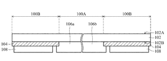
【解決手段】タッチデバイス100が提供される。タッチデバイス100は、感知領域100Aと、周辺領域100Bと、を有する。さらに、タッチデバイス100は、タッチ感知層(106b、112)と、タッチ感知層(106b、112)から離されて周辺領域100Bに配置される遮蔽層(108、114)と、タッチ感知層(106b、112)と遮蔽層(108、114)の間に配置される絶縁層110と、を含む。
【選択図】図2
Description
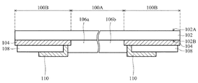
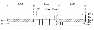
100A、200A 感知領域、
100B、200B 周辺領域、
102 基板、
102A 第1の面、
102B 第2の面、
104 マスク層、
106a、106b 感知電極、
108 誘導層、
110 絶縁層、
112 信号伝送線、
114 導電層、
116 保護層、
120Y 第1の感知電極、
120X 第2の感知電極、
122 絶縁部、
124 ブリッジ線、
132 ユーザの手、
140 ディスプレイパネル、
150、250 タッチパネル、
Claims (25)
- 感知領域と、前記感知領域を取り囲む周辺領域と、を有するタッチデバイスであって、
タッチ感知層と、
前記周辺領域に配置され、前記タッチ感知層から離されている遮蔽層と、
前記タッチ感知層および前記遮蔽層の間に配置される絶縁層と、を備える、
タッチデバイス。 - 前記タッチ感知層は、感知電極と、信号伝送線と、を備え、
前記感知電極の主要部分が前記感知領域に配置され、
前記信号伝送線が前記絶縁層上に配置され、
前記信号伝送線の主要部分が前記周辺領域に配置され、
前記信号伝送線が前記感知電極に電気的に接続される、
請求項1に記載のタッチデバイス。 - 前記遮蔽層は、誘導層と、導電層と、を備え、
前記導電層が前記誘導層上に配置され、かつ、前記誘導層に電気的に接続される、
請求項1または2に記載のタッチデバイス。 - 基板と、マスク層と、を更に備え、
前記マスク層が前記基板上であって、かつ、前記周辺領域に配置される、
請求項1〜3いずれか1項に記載のタッチデバイス。 - 前記遮蔽層の一部分が前記マスク層および前記絶縁層の間に配置される、
請求項1に記載のタッチデバイス。 - 感知領域と、前記感知領域を取り囲む周辺領域と、を有するタッチデバイスであって、
基板と、
前記基板上であって、かつ、前記感知領域に配置される感知電極と、
前記基板上であって、かつ、前記周辺領域に配置されるマスク層と、
前記感知電極に電気的に接続されて前記マスク層に覆われる信号伝送線と、
前記マスク層上に配置される誘導層と、
前記誘導層および前記信号伝送線の間であって、かつ、前記誘導層および前記感知電極の間に配置される絶縁層と、
前記誘導層上に配置され、かつ、前記誘導層に電気的に接続される導電層と、を備える、
タッチデバイス。 - 前記感知電極は、徐々に幅が減少される複数の第1の帯状パターンと、徐々に幅が増加される複数の第2の帯状パターンと、を有し、前記第1の帯状パターンと前記第2の帯状パターンとが交互に配置される、
請求項6に記載のタッチデバイス。 - 前記感知電極は、列に配置された複数の第1の感知電極と行に配置された複数の第2の感知電極と、を備え、前記複数の第1の感知電極はそれぞれ互いに接続され、前記複数の第2の感知電極はそれぞれ互いに離されている、
請求項6に記載のタッチデバイス。 - 任意の2つの隣接する前記第2の感知電極を電気的に接続するブリッジ線と、
前記第1の感知電極および前記ブリッジ線の間に配置される絶縁部と、を更に備える、
請求項8に記載のタッチデバイス。
- 前記マスク層、前記誘導層、および前記導電層の形状は、リング形状を用いる、
請求項6〜9いずれか1項に記載のタッチデバイス。 - 前記基板上に全体的に配置されて、前記感知電極、前記マスク層、前記信号伝送線、前記誘導層、および前記導電層を覆う保護層と、
前記保護層に貼りあわされるディスプレイパネルと、を更に備える、
請求項6〜10いずれか1項に記載のタッチデバイス。 - 前記誘導層は、前記信号線および前記マスク層の間に配置される、
請求項6〜11いずれか1項に記載のタッチデバイス。 - 感知領域と、前記感知領域を取り囲む周辺領域と、を有するタッチデバイスの製造方法であって、
タッチ感知層を形成するステップと、
前記タッチ感知層から離されており、前記周辺領域に配置される遮蔽層を形成するステップと、
前記タッチ感知層および前記遮蔽層の間に配置される絶縁層を形成するステップと、を備える、
タッチデバイスの製造方法。 - 前記タッチ感知層は、感知電極と、信号伝送線と、を備え、
前記感知電極の主要部分が前記感知領域に形成され、
前記信号伝送線が前記絶縁層上に形成され、
前記信号伝送線の主要部分が前記周辺領域に形成され、
前記信号伝送線が前記感知電極に電気的に接続される、
請求項13に記載のタッチデバイスの製造方法。 - 前記遮蔽層は、誘導層と、導電層と、を備え、
前記導電層が前記誘導層上に形成され、かつ、前記誘導層に電気的に接続される、
請求項13または14に記載のタッチデバイスの製造方法。 - 同一のプロセスが前記感知電極および前記誘導層を同時に形成する、
請求項15に記載のタッチデバイスの製造方法。 - 同一のプロセスが前記信号伝送線および前記導電層を同時に形成する、
請求項15または16に記載のタッチデバイスの製造方法。 - 前記絶縁層は、前記誘導層および前記感知電極の間であって、かつ、前記誘導層および前記信号伝送線の間に形成される、
請求項15〜17いずれか1項に記載のタッチデバイスの製造方法。 - 前記感知電極は、徐々に幅が減少される複数の第1の帯状パターンと、徐々に幅が増加される複数の第2の帯状パターンと、を備え、前記第1の帯状パターンと前記第2の帯状パターンとが交互に配置される、
請求項14に記載のタッチデバイスの製造方法。 - 前記感知電極を形成するステップは、
それぞれ互いに接続され、列に配置される複数の第1の感知電極を形成すること、
それぞれ互いに離され、行に配置される複数の第2の感知電極を形成すること、
同一行の任意の2つの隣接する前記第2の感知電極を電気的に接続するブリッジ線を形成すること、
前記第1の感知電極および前記ブリッジ線の間に絶縁部を形成すること、を備える、
請求項15〜18いずれか1項に記載のタッチデバイスの製造方法。 - 前記ブリッジ線、前記信号伝送線、および前記導電層は、同一のプロセスによって同時に形成される、
請求項20に記載のタッチデバイスの製造方法。 - 前記絶縁部および前記絶縁層は、同一のプロセスによって同時に形成される、
請求項20または21に記載のタッチデバイスの製造方法。 - 基板を提供すること、
前記基板上であって、かつ、前記周辺領域にマスク層を形成すること、を更に備える、
請求項13〜22いずれか1項に記載のタッチデバイスの製造方法。 - 前記遮蔽層は、前記マスク層および前記絶縁層の間に形成される、
請求項23に記載のタッチデバイスの製造方法。 - 前記タッチ感知層および前記遮蔽層を覆う保護層を覆うように形成すること、
前記保護層と貼りあわせるディスプレイパネルを提供すること、を更に備える、
請求項13〜24いずれか1項に記載のタッチデバイスの製造方法。
Applications Claiming Priority (2)
| Application Number | Priority Date | Filing Date | Title |
|---|---|---|---|
| CN201110077947.9 | 2011-03-18 | ||
| CN201110077947.9A CN102681712B (zh) | 2011-03-18 | 2011-03-18 | 触控装置及其制造方法 |
Publications (2)
| Publication Number | Publication Date |
|---|---|
| JP2012198885A true JP2012198885A (ja) | 2012-10-18 |
| JP5502919B2 JP5502919B2 (ja) | 2014-05-28 |
Family
ID=44789311
Family Applications (1)
| Application Number | Title | Priority Date | Filing Date |
|---|---|---|---|
| JP2012051643A Expired - Fee Related JP5502919B2 (ja) | 2011-03-18 | 2012-03-08 | タッチデバイス及びその製造方法 |
Country Status (6)
| Country | Link |
|---|---|
| US (1) | US8952903B2 (ja) |
| EP (1) | EP2500803A3 (ja) |
| JP (1) | JP5502919B2 (ja) |
| KR (1) | KR101365180B1 (ja) |
| CN (1) | CN102681712B (ja) |
| TW (2) | TWI459254B (ja) |
Cited By (2)
| Publication number | Priority date | Publication date | Assignee | Title |
|---|---|---|---|---|
| JP2014142692A (ja) * | 2013-01-22 | 2014-08-07 | Juhn Jong Lin | タッチパネルの製造方法 |
| JP2014224937A (ja) * | 2013-05-17 | 2014-12-04 | 大日本印刷株式会社 | 配線付き表示装置用前面保護板とその製造方法、及び表示装置 |
Families Citing this family (37)
| Publication number | Priority date | Publication date | Assignee | Title |
|---|---|---|---|---|
| CN102681709B (zh) * | 2011-03-17 | 2016-01-27 | 宸鸿光电科技股份有限公司 | 触控显示设备及其制造方法 |
| CN103049121B (zh) * | 2011-10-13 | 2016-04-06 | 宸鸿科技(厦门)有限公司 | 触控装置及其制造方法 |
| TWM425340U (en) * | 2011-10-21 | 2012-03-21 | Henghao Technology Co Ltd | Capacitive touch panel and touch display panel using the same |
| JP5189197B1 (ja) * | 2011-10-27 | 2013-04-24 | シャープ株式会社 | 携帯情報端末 |
| US9429608B2 (en) * | 2011-11-11 | 2016-08-30 | Plantronics, Inc. | Separation of capacitive touch areas |
| CN103164069B (zh) * | 2011-12-19 | 2016-02-24 | 瀚宇彩晶股份有限公司 | 触控装置及其制造方法 |
| US10159146B2 (en) * | 2012-01-18 | 2018-12-18 | Kyocera Corporation | Input apparatus, display apparatus, and electronic apparatus |
| JP2013152562A (ja) * | 2012-01-24 | 2013-08-08 | Japan Display West Co Ltd | タッチパネルおよびその製造方法、表示装置、ならびに電子機器 |
| GB2499987B (en) * | 2012-03-02 | 2017-01-11 | Novalia Ltd | Touch-sensitive input device |
| CN103425301B (zh) * | 2012-05-16 | 2016-10-05 | 宸鸿科技(厦门)有限公司 | 触控面板及其制作方法 |
| JP2015180979A (ja) * | 2012-07-31 | 2015-10-15 | シャープ株式会社 | タッチパネルおよびタッチパネルの製造方法 |
| US20140092023A1 (en) * | 2012-09-28 | 2014-04-03 | Htc Corporation | Touch display module and handheld electronic apparatus |
| US9529462B2 (en) * | 2012-10-29 | 2016-12-27 | Sharp Kabushiki Kaisha | Touch panel |
| CN103092411A (zh) * | 2013-01-10 | 2013-05-08 | 北京京东方光电科技有限公司 | 一种触摸屏及其制作方法、显示装置 |
| TWI498780B (zh) * | 2013-01-22 | 2015-09-01 | Henghao Technology Co Ltd | 觸控面板 |
| TWI488084B (zh) | 2013-02-08 | 2015-06-11 | Acer Inc | 觸控面板 |
| JP2014154088A (ja) * | 2013-02-13 | 2014-08-25 | Geomatec Co Ltd | 保護パネル一体型タッチパネルセンサ,その製造方法及び携帯用電子機器 |
| CN104007864B (zh) * | 2013-02-27 | 2017-09-12 | 宸鸿科技(厦门)有限公司 | 触控面板及其制作方法 |
| CN103176660B (zh) * | 2013-03-28 | 2015-09-30 | 南昌欧菲光科技有限公司 | 位置传感器 |
| US9606679B2 (en) | 2013-04-23 | 2017-03-28 | Industrial Technology Research Institute | Touch panel and manufacturing method thereof and touch display panel |
| TWI486841B (zh) | 2013-06-26 | 2015-06-01 | Young Lighting Technology Inc | 觸控模組 |
| FR3008809B1 (fr) | 2013-07-18 | 2017-07-07 | Fogale Nanotech | Dispositif accessoire garde pour un appareil electronique et/ou informatique, et appareil equipe d'un tel dispositif accessoire |
| US9433102B2 (en) | 2013-08-30 | 2016-08-30 | Boe Technology Group Co., Ltd. | Touch screen panel and method for manufacturing the same, and display device |
| CN103455203A (zh) * | 2013-08-30 | 2013-12-18 | 京东方科技集团股份有限公司 | 触摸屏、其制作方法及显示装置 |
| CN103500036B (zh) * | 2013-08-30 | 2015-04-29 | 京东方科技集团股份有限公司 | 触摸屏的制作方法 |
| CN103455204B (zh) * | 2013-08-30 | 2016-08-17 | 京东方科技集团股份有限公司 | 触摸屏、其制作方法及显示装置 |
| US9430109B2 (en) | 2013-08-30 | 2016-08-30 | Boe Technology Group Co., Ltd. | Touch screen panel and method for manufacturing the same, and display device |
| KR102119818B1 (ko) * | 2013-09-24 | 2020-06-05 | 엘지이노텍 주식회사 | 터치 패널 |
| US9292141B2 (en) * | 2013-10-30 | 2016-03-22 | Apple Inc. | Double sided touch sensor on transparent substrate |
| FR3013472B1 (fr) | 2013-11-19 | 2016-07-08 | Fogale Nanotech | Dispositif accessoire couvrant pour un appareil portable electronique et/ou informatique, et appareil equipe d'un tel dispositif accessoire |
| TW201545030A (zh) * | 2014-05-30 | 2015-12-01 | Henghao Technology Co Ltd | 觸控面板及其形成方法 |
| CN105528122A (zh) * | 2014-09-29 | 2016-04-27 | 宸鸿科技(厦门)有限公司 | 触控面板及其制造方法 |
| CN105786230B (zh) * | 2014-12-23 | 2019-08-13 | 宸鸿科技(厦门)有限公司 | 触控面板及其制造方法 |
| CN105653107B (zh) * | 2015-12-28 | 2020-09-01 | 昆山龙腾光电股份有限公司 | 触控装置、电子装置以及手机 |
| KR102512040B1 (ko) * | 2016-05-04 | 2023-03-20 | 엘지디스플레이 주식회사 | 플렉서블 디스플레이 패널 및 그 제조 방법 |
| CN106843616B (zh) * | 2017-01-03 | 2020-05-19 | 京东方科技集团股份有限公司 | 一种触控基板及其制作方法、触控显示装置 |
| CN110389686B (zh) * | 2019-07-25 | 2023-09-08 | 京东方科技集团股份有限公司 | 一种触控器件、显示装置以及触控器件的制备方法 |
Citations (3)
| Publication number | Priority date | Publication date | Assignee | Title |
|---|---|---|---|---|
| JP2009169720A (ja) * | 2008-01-17 | 2009-07-30 | Smk Corp | タッチセンサ |
| JP2009193587A (ja) * | 2008-02-18 | 2009-08-27 | Tpk Touch Solutions Inc | 静電容量タッチパネル |
| JP2011048780A (ja) * | 2009-08-28 | 2011-03-10 | Kyocera Corp | 入力装置およびこれを備える表示装置 |
Family Cites Families (18)
| Publication number | Priority date | Publication date | Assignee | Title |
|---|---|---|---|---|
| US5579036A (en) * | 1994-04-28 | 1996-11-26 | At&T Global Information Solutions Company | Touch screen device and shielding bracket therefor |
| US5548306A (en) * | 1994-04-28 | 1996-08-20 | At&T Global Information Solutions Company | Visible and touchable touch screen shield |
| KR100659048B1 (ko) * | 2000-09-06 | 2006-12-18 | 삼성에스디아이 주식회사 | 외부 노이즈를 차단할 수 있는 더미전극을 구비한 터치패널 |
| CN101449461B (zh) * | 2006-03-13 | 2013-06-12 | 艾登特技术股份公司 | 电容传感器设备 |
| TW200805128A (en) * | 2006-05-05 | 2008-01-16 | Harald Philipp | Touch screen element |
| US20080001926A1 (en) * | 2006-06-29 | 2008-01-03 | Xiaoping Jiang | Bidirectional slider |
| US8610690B2 (en) * | 2007-07-27 | 2013-12-17 | Tpk Touch Solutions Inc. | Capacitive sensor and method for manufacturing same |
| KR100921813B1 (ko) * | 2007-11-07 | 2009-10-16 | 주식회사 애트랩 | 터치 패널 장치 및 이의 접촉위치 검출방법 |
| CN201174007Y (zh) | 2008-03-18 | 2008-12-31 | 宸鸿光电科技股份有限公司 | 电容式触控面板 |
| US8629842B2 (en) * | 2008-07-11 | 2014-01-14 | Samsung Display Co., Ltd. | Organic light emitting display device |
| KR20100065486A (ko) * | 2008-12-08 | 2010-06-17 | 주식회사 엔에이치케이플러스 | 정전용량 방식의 터치 패널 구조 |
| TWI373665B (en) * | 2008-12-25 | 2012-10-01 | Au Optronics Corp | Touch panel structure |
| JP5337061B2 (ja) * | 2009-02-20 | 2013-11-06 | セイコーインスツル株式会社 | タッチパネル及びこれを備える表示装置 |
| TWM361675U (en) | 2009-02-24 | 2009-07-21 | Sentelic Corp | Thin film touch panel |
| CN201387599Y (zh) | 2009-03-05 | 2010-01-20 | 升达科技股份有限公司 | 薄膜触控板 |
| CN201465086U (zh) | 2009-07-03 | 2010-05-12 | 深圳市汇顶科技有限公司 | 一种抗干扰的电容式触摸屏及电子设备 |
| JP5300640B2 (ja) * | 2009-07-27 | 2013-09-25 | 株式会社ジャパンディスプレイウェスト | 静電容量型入力装置および入力装置付き電気光学装置 |
| CN202041932U (zh) * | 2011-03-18 | 2011-11-16 | 宸鸿科技(厦门)有限公司 | 触控装置 |
-
2011
- 2011-03-18 CN CN201110077947.9A patent/CN102681712B/zh not_active Expired - Fee Related
- 2011-05-31 TW TW100118980A patent/TWI459254B/zh not_active IP Right Cessation
- 2011-05-31 TW TW100209811U patent/TWM414620U/zh not_active IP Right Cessation
- 2011-08-09 US US13/205,630 patent/US8952903B2/en active Active
- 2011-08-22 EP EP11178253.8A patent/EP2500803A3/en not_active Ceased
- 2011-08-31 KR KR1020110088016A patent/KR101365180B1/ko not_active Expired - Fee Related
-
2012
- 2012-03-08 JP JP2012051643A patent/JP5502919B2/ja not_active Expired - Fee Related
Patent Citations (3)
| Publication number | Priority date | Publication date | Assignee | Title |
|---|---|---|---|---|
| JP2009169720A (ja) * | 2008-01-17 | 2009-07-30 | Smk Corp | タッチセンサ |
| JP2009193587A (ja) * | 2008-02-18 | 2009-08-27 | Tpk Touch Solutions Inc | 静電容量タッチパネル |
| JP2011048780A (ja) * | 2009-08-28 | 2011-03-10 | Kyocera Corp | 入力装置およびこれを備える表示装置 |
Cited By (2)
| Publication number | Priority date | Publication date | Assignee | Title |
|---|---|---|---|---|
| JP2014142692A (ja) * | 2013-01-22 | 2014-08-07 | Juhn Jong Lin | タッチパネルの製造方法 |
| JP2014224937A (ja) * | 2013-05-17 | 2014-12-04 | 大日本印刷株式会社 | 配線付き表示装置用前面保護板とその製造方法、及び表示装置 |
Also Published As
| Publication number | Publication date |
|---|---|
| KR101365180B1 (ko) | 2014-02-21 |
| US8952903B2 (en) | 2015-02-10 |
| US20120235927A1 (en) | 2012-09-20 |
| CN102681712B (zh) | 2016-08-24 |
| EP2500803A3 (en) | 2014-02-26 |
| JP5502919B2 (ja) | 2014-05-28 |
| TWI459254B (zh) | 2014-11-01 |
| EP2500803A2 (en) | 2012-09-19 |
| CN102681712A (zh) | 2012-09-19 |
| TW201239700A (en) | 2012-10-01 |
| TWM414620U (en) | 2011-10-21 |
| KR20120106526A (ko) | 2012-09-26 |
Similar Documents
| Publication | Publication Date | Title |
|---|---|---|
| JP5502919B2 (ja) | タッチデバイス及びその製造方法 | |
| TWI386838B (zh) | 觸控顯示面板與觸控基材 | |
| US20100283757A1 (en) | Capacitive touch panel structure with high optical uniformity | |
| US8847906B2 (en) | Touch device and method for manufacturing the same | |
| EP2770409B1 (en) | Touch panel and manufacturing method thereof | |
| US8339527B2 (en) | Thin touch panel | |
| US9626052B2 (en) | Touch panel | |
| KR101960532B1 (ko) | 표시장치용 정전용량 방식 터치 스크린 패널 및 그 제조방법 | |
| TWI476655B (zh) | 觸控裝置及其製造方法 | |
| KR101719368B1 (ko) | 정전용량 방식 터치 스크린 패널 및 그 제조방법 | |
| CN102253752B (zh) | 触摸面板以及触摸显示面板 | |
| TWI421756B (zh) | 觸控顯示面板及觸控面板 | |
| KR101475106B1 (ko) | 정전용량 방식 터치 스크린 패널 및 그 제조방법 | |
| US20140347319A1 (en) | Touch panel | |
| EP2209065A2 (en) | Touch screen panel and method for fabricating the same | |
| US20150085205A1 (en) | Touch panel | |
| JP2011186717A (ja) | 静電容量型タッチパネルとその製造方法 | |
| WO2018028161A1 (zh) | 触控基板及其制作方法、显示面板和显示装置 | |
| US20120139852A1 (en) | Touch panel and touch display panel having the same | |
| CN103543866A (zh) | 触控面板及其制作方法与触控显示面板 | |
| US8120589B2 (en) | Touch panel | |
| CN202041932U (zh) | 触控装置 | |
| WO2014015618A1 (zh) | 触控面板及其制造方法、触控设备 | |
| JP2013015989A (ja) | 静電容量型タッチパネルとその製造方法 | |
| CN204515734U (zh) | 触控面板 |
Legal Events
| Date | Code | Title | Description |
|---|---|---|---|
| A977 | Report on retrieval |
Free format text: JAPANESE INTERMEDIATE CODE: A971007 Effective date: 20130117 |
|
| A131 | Notification of reasons for refusal |
Free format text: JAPANESE INTERMEDIATE CODE: A131 Effective date: 20130129 |
|
| A521 | Request for written amendment filed |
Free format text: JAPANESE INTERMEDIATE CODE: A523 Effective date: 20130426 |
|
| A131 | Notification of reasons for refusal |
Free format text: JAPANESE INTERMEDIATE CODE: A131 Effective date: 20130723 |
|
| A521 | Request for written amendment filed |
Free format text: JAPANESE INTERMEDIATE CODE: A523 Effective date: 20131016 |
|
| A131 | Notification of reasons for refusal |
Free format text: JAPANESE INTERMEDIATE CODE: A131 Effective date: 20131119 |
|
| A521 | Request for written amendment filed |
Free format text: JAPANESE INTERMEDIATE CODE: A523 Effective date: 20140205 |
|
| TRDD | Decision of grant or rejection written | ||
| A01 | Written decision to grant a patent or to grant a registration (utility model) |
Free format text: JAPANESE INTERMEDIATE CODE: A01 Effective date: 20140225 |
|
| A61 | First payment of annual fees (during grant procedure) |
Free format text: JAPANESE INTERMEDIATE CODE: A61 Effective date: 20140313 |
|
| R150 | Certificate of patent or registration of utility model |
Ref document number: 5502919 Country of ref document: JP Free format text: JAPANESE INTERMEDIATE CODE: R150 |
|
| R250 | Receipt of annual fees |
Free format text: JAPANESE INTERMEDIATE CODE: R250 |
|
| R250 | Receipt of annual fees |
Free format text: JAPANESE INTERMEDIATE CODE: R250 |
|
| R250 | Receipt of annual fees |
Free format text: JAPANESE INTERMEDIATE CODE: R250 |
|
| R250 | Receipt of annual fees |
Free format text: JAPANESE INTERMEDIATE CODE: R250 |
|
| R250 | Receipt of annual fees |
Free format text: JAPANESE INTERMEDIATE CODE: R250 |
|
| R250 | Receipt of annual fees |
Free format text: JAPANESE INTERMEDIATE CODE: R250 |
|
| R250 | Receipt of annual fees |
Free format text: JAPANESE INTERMEDIATE CODE: R250 |
|
| R250 | Receipt of annual fees |
Free format text: JAPANESE INTERMEDIATE CODE: R250 |
|
| LAPS | Cancellation because of no payment of annual fees |