JP2012199466A - Power module - Google Patents

Power module Download PDF

Info

Publication number
JP2012199466A
JP2012199466A JP2011063676A JP2011063676A JP2012199466A JP 2012199466 A JP2012199466 A JP 2012199466A JP 2011063676 A JP2011063676 A JP 2011063676A JP 2011063676 A JP2011063676 A JP 2011063676A JP 2012199466 A JP2012199466 A JP 2012199466A
Authority
JP
Japan
Prior art keywords
power module
noise
semiconductor elements
loop coil
noise absorber
Prior art date
Legal status (The legal status is an assumption and is not a legal conclusion. Google has not performed a legal analysis and makes no representation as to the accuracy of the status listed.)
Pending
Application number
JP2011063676A
Other languages
Japanese (ja)
Inventor
Yuichiro Sugano
雄一郎 菅野
Current Assignee (The listed assignees may be inaccurate. Google has not performed a legal analysis and makes no representation or warranty as to the accuracy of the list.)
Nissan Motor Co Ltd
Original Assignee
Nissan Motor Co Ltd
Priority date (The priority date is an assumption and is not a legal conclusion. Google has not performed a legal analysis and makes no representation as to the accuracy of the date listed.)
Filing date
Publication date
Application filed by Nissan Motor Co Ltd filed Critical Nissan Motor Co Ltd
Priority to JP2011063676A priority Critical patent/JP2012199466A/en
Publication of JP2012199466A publication Critical patent/JP2012199466A/en
Pending legal-status Critical Current

Links

Images

Classifications

    • HELECTRICITY
    • H10SEMICONDUCTOR DEVICES; ELECTRIC SOLID-STATE DEVICES NOT OTHERWISE PROVIDED FOR
    • H10WGENERIC PACKAGES, INTERCONNECTIONS, CONNECTORS OR OTHER CONSTRUCTIONAL DETAILS OF DEVICES COVERED BY CLASS H10
    • H10W72/00Interconnections or connectors in packages
    • H10W72/50Bond wires
    • H10W72/541Dispositions of bond wires
    • H10W72/5445Dispositions of bond wires being orthogonal to a side surface of the chip, e.g. parallel arrangements
    • HELECTRICITY
    • H10SEMICONDUCTOR DEVICES; ELECTRIC SOLID-STATE DEVICES NOT OTHERWISE PROVIDED FOR
    • H10WGENERIC PACKAGES, INTERCONNECTIONS, CONNECTORS OR OTHER CONSTRUCTIONAL DETAILS OF DEVICES COVERED BY CLASS H10
    • H10W74/00Encapsulations, e.g. protective coatings

Landscapes

  • Inverter Devices (AREA)

Abstract

【課題】半導体素子の寄生容量と、半導体素子同士を接続するワイヤのインダクタンスとの間の共振で発生するノイズを低減し得るパワーモジュールを提供する。
【解決手段】複数の半導体素子(11、12)と、複数の半導体素子(11、12)を接続するワイヤ(36、37、39)と、ループコイル(52)及び磁性体(53)からなるノイズ吸収体(51)とを有し、このノイズ吸収体(51)を複数の半導体素子(11、12)の少なくとも1つの近傍に配置すると共に、ループコイル(52)のループ面を、複数の半導体素子(11、12)を接続するワイヤのうちノイズが発生するワイヤ(36、37)の少なくとも1つに沿わせて配置する。
【選択図】図2
A power module capable of reducing noise generated by resonance between a parasitic capacitance of a semiconductor element and an inductance of a wire connecting the semiconductor elements.
A plurality of semiconductor elements (11, 12), wires (36, 37, 39) connecting the plurality of semiconductor elements (11, 12), a loop coil (52), and a magnetic body (53). A noise absorber (51), the noise absorber (51) is disposed in the vicinity of at least one of the plurality of semiconductor elements (11, 12), and the loop surface of the loop coil (52) Of the wires connecting the semiconductor elements (11, 12), the wires are arranged along at least one of the wires (36, 37) that generate noise.
[Selection] Figure 2

Description

この発明はパワーモジュール(電力変換器)の電磁両立性に関するものである。   The present invention relates to electromagnetic compatibility of a power module (power converter).

パワーモジュールからの放射ノイズを低減するため、半導体素子から引き出された電極を個別のノイズ吸収体で囲み、かつ、ノイズ吸収体を半導体素子保護用のゲル質の封止材中に埋設する技術が開示されている(特許文献1参照)。   In order to reduce the radiation noise from the power module, there is a technology that surrounds the electrode drawn from the semiconductor element with an individual noise absorber and embeds the noise absorber in a gelatinous sealing material for protecting the semiconductor element It is disclosed (see Patent Document 1).

特開2004−207432号公報JP 2004-207432 A

ところで、パワーモジュール内で複数の半導体素子を接続する構成においては、半導体素子の寄生容量と、半導体素子同士を接続するワイヤのインダクタンスとの間の共振でノイズが発生する。   Incidentally, in a configuration in which a plurality of semiconductor elements are connected in a power module, noise is generated due to resonance between the parasitic capacitance of the semiconductor elements and the inductance of the wire connecting the semiconductor elements.

しかしながら、上記特許文献1の技術では、このノイズに対して、ノイズを低減する効果がないという問題点がある。   However, the technique of Patent Document 1 has a problem in that there is no effect of reducing noise against this noise.

そこで本発明は、半導体素子の寄生容量と、半導体素子同士を接続するワイヤのインダクタンスとの間の共振で発生するノイズを低減し得るパワーモジュールを提供することを目的とする。   Therefore, an object of the present invention is to provide a power module that can reduce noise generated by resonance between the parasitic capacitance of a semiconductor element and the inductance of a wire connecting the semiconductor elements.

本発明のパワーモジュールは、複数の半導体素子と、これら複数の半導体素子を接続するワイヤと、ループコイル及び磁性体からなるノイズ吸収体とを有している。そして、このノイズ吸収体を前記複数の半導体素子の少なくとも1つの近傍に配置すると共に、前記ループコイルのループ面を、前記複数の半導体素子を接続するワイヤのうちノイズが発生するワイヤの少なくとも1つに沿わせて配置している。   The power module of the present invention includes a plurality of semiconductor elements, wires connecting the plurality of semiconductor elements, and a noise absorber made of a loop coil and a magnetic material. The noise absorber is disposed in the vicinity of at least one of the plurality of semiconductor elements, and the loop surface of the loop coil is disposed on at least one of the wires generating noise among the wires connecting the plurality of semiconductor elements. It is arranged along.

本発明によれば、ループコイルはノイズ源となる共振回路(複数の半導体素子の寄生容量と、半導体素子同士を接続するワイヤインダクタンスとからなる回路)に磁気的に結合し、磁性体の抵抗分によってノイズ成分を減衰することができる。   According to the present invention, the loop coil is magnetically coupled to a resonance circuit (a circuit including a parasitic capacitance of a plurality of semiconductor elements and a wire inductance connecting the semiconductor elements) as a noise source, and a resistance component of the magnetic body. The noise component can be attenuated.

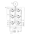
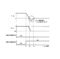
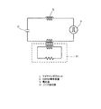
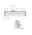
本発明の第1実施形態のモータ駆動用3相インバータの回路図である。It is a circuit diagram of the three-phase inverter for motor drive of a 1st embodiment of the present invention. 第1実施形態の1つのパワーモジュールの一部の実装状態での概略断面図である。It is a schematic sectional drawing in the mounting state of a part of one power module of 1st Embodiment. 第1実施形態の1つのパワーモジュールの一部の実装状態での素子配置を示す概略平面図である。It is a schematic plan view which shows element arrangement | positioning in the mounting state of a part of one power module of 1st Embodiment. 1つのパワーモジュールの回路動作図である。It is a circuit operation | movement figure of one power module. パワーモジュール内部でのノイズの発生を説明するためのタイミングチャートである。It is a timing chart for demonstrating generation | occurrence | production of the noise inside a power module. ノイズ源となる共振回路の等価回路図である。It is an equivalent circuit diagram of the resonance circuit used as a noise source. 第2実施形態の1つのパワーモジュールの一部の実装状態での概略断面図である。It is a schematic sectional drawing in the mounting state of a part of one power module of 2nd Embodiment. 第2実施形態の1つのパワーモジュールの一部の実装状態での素子配置を示す概略平面図である。It is a schematic plan view which shows element arrangement | positioning in the mounting state of a part of one power module of 2nd Embodiment. 第3実施形態の1つのパワーモジュールの一部の実装状態での概略断面図である。It is a schematic sectional drawing in the mounting state of a part of one power module of 3rd Embodiment. 第3実施形態の1つのパワーモジュールの一部の実装状態での素子配置を示す概略平面図である。It is a schematic plan view which shows element arrangement | positioning in the mounting state of a part of one power module of 3rd Embodiment.

以下、本発明の実施形態を図面に基づき説明する。   Hereinafter, embodiments of the present invention will be described with reference to the drawings.

(第1実施形態)
図1は本発明の第1実施形態に係るパワーモジュール10を備えたモータ駆動用3相インバータ14の回路図である。図1に示すように、1つのパワーモジュール10は、スイッチング素子としてのIGBT(Insuated Gate Bipolar Transistor)11及び整流素子としての還流ダイオード12を有し、各還流ダイオード12は、各IGBT11と逆並列に接続されている。このパワーモジュール10は、交流モータ13を駆動するための3相インバータ14の1相分(1アーム分)である。直流電源15の電力は、平滑用のコンデンサ16と3個のパワーモジュール10により、自動車用の交流モータ13を駆動する3相交流電力に変換される。
(First embodiment)
FIG. 1 is a circuit diagram of a three-phase inverter 14 for driving a motor provided with a power module 10 according to the first embodiment of the present invention. As shown in FIG. 1, one power module 10 has an IGBT (Insuated Gate Bipolar Transistor) 11 as a switching element and a free-wheeling diode 12 as a rectifying element, and each free-wheeling diode 12 is antiparallel to each IGBT 11. It is connected. This power module 10 is for one phase (one arm) of a three-phase inverter 14 for driving the AC motor 13. The electric power of the DC power supply 15 is converted by the smoothing capacitor 16 and the three power modules 10 into three-phase AC power for driving the automotive AC motor 13.

詳細には、インバータには、交流モータ13とインバータ14を接続する外部バスバー(出力側)21、直流電源15とインバータ14を接続する外部バスバー(P側)22及び外部バスバー(N側)23を備えている。1つのパワーモジュール10には、外部バスバー(出力側)21と接続する出力電極24、外部バスバー(P側)22と接続するP型電極25及び外部バスバー(N側)23と接続するN型電極26を備えている。   Specifically, the inverter includes an external bus bar (output side) 21 that connects the AC motor 13 and the inverter 14, an external bus bar (P side) 22 that connects the DC power supply 15 and the inverter 14, and an external bus bar (N side) 23. I have. One power module 10 includes an output electrode 24 connected to an external bus bar (output side) 21, a P-type electrode 25 connected to an external bus bar (P side) 22, and an N-type electrode connected to an external bus bar (N side) 23. 26.

図2は1つのパワーモジュール10の一部の実装状態での概略断面図、図3は1つのパワーモジュール10の一部の実装状態での素子配置を示す概略平面図である。図1には3つのパワーモジュール10が示されているが、各パワーモジュール10の構成は3つとも同じである。図2においては上方が鉛直上方であるとする。従って、全体として平板状のパワーモジュール10は水平な位置に置かれている。なお、図3においては、図2に示した封止材40及び樹脂蓋41を取り去った状態を示している。   FIG. 2 is a schematic sectional view of a part of one power module 10 in a mounted state, and FIG. 3 is a schematic plan view showing an element arrangement in a part of the mounted state of one power module 10. Although three power modules 10 are shown in FIG. 1, the configuration of each power module 10 is the same for all three. In FIG. 2, it is assumed that the upper side is the vertical upper side. Therefore, the flat power module 10 as a whole is placed in a horizontal position. 3 shows a state where the sealing material 40 and the resin lid 41 shown in FIG. 2 are removed.

図1の回路図においては1つのパワーモジュール10について、IGBT11と還流ダイオード12とを逆並列に接続した複数の半導体素子(この複数の半導体素子を以下「複数半導体素子」という。)が上下に2つ並んでいる。一方、図3に示す実装状態では、図1に示した上下2つの複数半導体素子の一方(1つのパワーモジュール10の一部)について、3つのIGBT11a〜11cと、3つの還流ダイオード12a〜12cとが用いられている。すなわち、図3において3つの複数半導体素子を縦方向にほぼ等間隔で並べ、これら3つの複数半導体素子を電気的に並列接続している。図示しないが、図3の下方(あるいは上方)には図1に示した上下2つの複数半導体素子の他方について、3つのIGBTと3つの還流ダイオードとが用いられている。このように、複数半導体素子を3つ並列接続している理由は、パワーモジュール10の電流容量をアップするためである。並列接続する複数半導体の数は3つに限定されるものでない。   In the circuit diagram of FIG. 1, for a single power module 10, a plurality of semiconductor elements (hereinafter referred to as “multiple semiconductor elements”) in which an IGBT 11 and a free-wheeling diode 12 are connected in antiparallel are two vertically. Are lined up. On the other hand, in the mounting state shown in FIG. 3, three IGBTs 11 a to 11 c, three free-wheeling diodes 12 a to 12 c, and one of the two upper and lower semiconductor elements shown in FIG. 1 (part of one power module 10) Is used. That is, in FIG. 3, three semiconductor elements are arranged in the vertical direction at substantially equal intervals, and these three semiconductor elements are electrically connected in parallel. Although not shown in the figure, three IGBTs and three free-wheeling diodes are used for the other of the upper and lower two semiconductor elements shown in FIG. Thus, the reason why three semiconductor elements are connected in parallel is to increase the current capacity of the power module 10. The number of semiconductors connected in parallel is not limited to three.

図2に示す実装状態では、1つのIGBT11及び1つの還流ダイオード12だけが見えている。図2において「複数半導体素子」といった場合、図3の上段に位置する複数半導体素子11a、12a、中段に位置する複数半導体素子11b、12b、下段に位置する複数半導体素子11c、12cの3つのうちのいずれか1つを意味している。図2において他の部材(36、37、38、39)及び後述するノイズ吸収体51についても同様である。   In the mounted state shown in FIG. 2, only one IGBT 11 and one free wheeling diode 12 are visible. In the case of “multiple semiconductor elements” in FIG. 2, among the three semiconductor elements 11a and 12a located in the upper stage of FIG. 3, the multiple semiconductor elements 11b and 12b located in the middle stage, and the multiple semiconductor elements 11c and 12c located in the lower stage. Any one of them. The same applies to the other members (36, 37, 38, 39) in FIG. 2 and the noise absorber 51 described later.

図2から説明する。1つのパワーモジュール10は、ベースプレート31、出力電極、P型電極及びN型電極を有するセラミック基板32、樹脂ケース33、セラミック基板32の鉛直上部に配置(実装)される複数半導体素子11、12などから構成される。これら複数半導体素子11、12を冷却する目的で冷却器(図示しない)も備えられている。   It demonstrates from FIG. One power module 10 includes a base plate 31, a ceramic substrate 32 having an output electrode, a P-type electrode and an N-type electrode, a resin case 33, a plurality of semiconductor elements 11, 12 arranged (mounted) vertically above the ceramic substrate 32, etc. Consists of A cooler (not shown) is also provided for the purpose of cooling the semiconductor elements 11 and 12.

IGBT11のコレクタ端子及び還流ダイオード12のカソード端子は、その鉛直下端が図示しないハンダによってセラミック基板32の出力電極に電気的に導通可能に接合される。また、IGBT11のエミッタ端子はボンディングワイヤ36によりセラミック基板32のN型電極に接合される。還流ダイオード12のアノード端子もボンディングワイヤ37によりセラミック基板32のN型電極に電気的に導通可能に接合される。さらにベースプレート31の外周に立設されている樹脂ケース33に外部端子38が固定され、この外部端子38とIGBT11のベース端子とがボンディングワイヤ39により接続されている。以下、ボンディングワイヤ36を「エミッタ接続ワイヤ」ともいう。ボンディングワイヤ37を「アノード接続ワイヤ」ともいう。   The collector terminal of the IGBT 11 and the cathode terminal of the free-wheeling diode 12 are joined to the output electrode of the ceramic substrate 32 by a solder (not shown) so that the lower end of the vertical terminal is electrically conductive. The emitter terminal of the IGBT 11 is joined to the N-type electrode of the ceramic substrate 32 by a bonding wire 36. The anode terminal of the reflux diode 12 is also bonded to the N-type electrode of the ceramic substrate 32 by the bonding wire 37 so as to be electrically conductive. Further, an external terminal 38 is fixed to a resin case 33 erected on the outer periphery of the base plate 31, and the external terminal 38 and the base terminal of the IGBT 11 are connected by a bonding wire 39. Hereinafter, the bonding wire 36 is also referred to as an “emitter connection wire”. The bonding wire 37 is also referred to as an “anode connection wire”.

複数半導体素子11、12の表面が空気中の湿気や酸素に触れて酸化したり腐食したりしないように、ゲル状の樹脂である封止材40によって樹脂ケース33内部が封止され、樹脂蓋41によって鉛直上部が蓋をされている。   The inside of the resin case 33 is sealed with a sealing material 40 that is a gel-like resin so that the surfaces of the plurality of semiconductor elements 11 and 12 do not oxidize or corrode when exposed to moisture or oxygen in the air. A vertical upper portion is covered with 41.

このように、インバータ14の主回路を構成する複数半導体素子11、12を配置し、ボンディングワイヤ36、37、39によって接続端子への配線を施し樹脂材等で封止したものがパワーモジュール10である。このパワーモジュール10を複数組合せてインバータ14を構成する。外部バスバー(出力側)21に流れる電流をIGBT11でスイッチングして、インバータ14が出力する電流をコントロールする。   In this way, the power module 10 is formed by arranging the plurality of semiconductor elements 11 and 12 constituting the main circuit of the inverter 14, wiring the connection terminals with the bonding wires 36, 37, and 39 and sealing them with a resin material or the like. is there. An inverter 14 is configured by combining a plurality of power modules 10. The current flowing through the external bus bar (output side) 21 is switched by the IGBT 11 to control the current output from the inverter 14.

この場合に、複数半導体素子11、12に寄生する容量(寄生容量)と、複数半導体素子11、12を接続するボンディングワイヤ36、37のインダクタンスとで共振する回路(この回路網を、以下「共振回路」という。)が存在する。このため、IGBT11がスイッチングすると、複数半導体素子11、12の寄生容量とボンディングワイヤ36、37のインダクタンスと間の共振でノイズが発生し、周囲に放射される。放射ノイズが発生すると、パワーモジュール10を組み合わせて構成されるインバータ14が電気自動車やハイブリッド車のモータ駆動用に用いられているときには、電子機器(車載環境ではラジオ)に悪影響を与えることが懸念される。   In this case, a circuit that resonates with the capacitance (parasitic capacitance) parasitic to the plurality of semiconductor elements 11 and 12 and the inductance of the bonding wires 36 and 37 that connect the plurality of semiconductor elements 11 and 12 (hereinafter, this circuit network is referred to as “resonance”). Circuit "). For this reason, when the IGBT 11 is switched, noise is generated due to resonance between the parasitic capacitances of the plurality of semiconductor elements 11 and 12 and the inductances of the bonding wires 36 and 37 and is emitted to the surroundings. When radiation noise is generated, there is a concern that when the inverter 14 configured by combining the power modules 10 is used for driving a motor of an electric vehicle or a hybrid vehicle, it adversely affects an electronic device (radio in an in-vehicle environment). The

この問題に対処するため、半導体素子から引き出された電極を個別のノイズ吸収体で囲み、かつノイズ吸収体を半導体素子素子保護用のゲル質の封止材中に埋設することで、放射ノイズを低減させる従来技術がある。   In order to cope with this problem, the electrodes drawn from the semiconductor element are surrounded by individual noise absorbers, and the noise absorbers are embedded in a gelatinous sealing material for protecting the semiconductor element elements, thereby reducing radiation noise. There are conventional techniques to reduce.

しかしながら、従来技術を本実施形態のパワーモジュール10に適用しても、複数半導体素子11、12の寄生容量と、複数半導体素子11、12を接続するボンディングワイヤの36、37のインダクタンスとの間の共振で発生するノイズを低減する効果が無い。なぜなら、従来技術の場合、複数半導体素子11、12から引き出された電極を個別のノイズ吸収体で囲んだとしても、複数半導体素子11、12を接続するボンディングワイヤ36、37は、前記電極を経由しないので、ノイズ低減効果がないためである。   However, even when the conventional technique is applied to the power module 10 of the present embodiment, the parasitic capacitance between the plurality of semiconductor elements 11 and 12 and the inductance of the bonding wires 36 and 37 connecting the plurality of semiconductor elements 11 and 12 are reduced. There is no effect of reducing noise generated by resonance. This is because, in the case of the prior art, even if the electrodes drawn from the plurality of semiconductor elements 11 and 12 are surrounded by individual noise absorbers, the bonding wires 36 and 37 connecting the plurality of semiconductor elements 11 and 12 pass through the electrodes. This is because there is no noise reduction effect.

そこで本発明の第1実施形態では、ノイズ吸収体51をループコイル52とフェライトビーズ53(磁性体)から構成する。このノイズ吸収体51をIGBT11と還流ダイオード12の少なくとも一方の近傍に配置する。さらに、ループコイル52のループ面を、複数半導体素子11、12を接続するワイヤのうちノイズが発生するボンディングワイヤ36、37の少なくとも一方に沿わせて配置する。   Therefore, in the first embodiment of the present invention, the noise absorber 51 is composed of a loop coil 52 and a ferrite bead 53 (magnetic material). The noise absorber 51 is disposed in the vicinity of at least one of the IGBT 11 and the free wheeling diode 12. Further, the loop surface of the loop coil 52 is disposed along at least one of the bonding wires 36 and 37 that generate noise among the wires connecting the plurality of semiconductor elements 11 and 12.

具体的に説明する。複数半導体素子11、12を接続するボンディングワイヤのうちノイズが発生するボンディングワイヤは、IGBT11のエミッタ接続ワイヤ36、還流ダイオード12のアノード接続ワイヤ37の2つある。いずれのワイヤ36、37とも5本ずつあり、図2に示したように鉛直上方に向けて凸の曲線を描いているため、これら5本ずつのエミッタ接続ワイヤ36及びアノード接続ワイヤ37よりノイズが周囲に放射される。   This will be specifically described. Of the bonding wires connecting the plurality of semiconductor elements 11 and 12, there are two bonding wires that generate noise, namely, an emitter connection wire 36 of the IGBT 11 and an anode connection wire 37 of the reflux diode 12. Since each of the wires 36 and 37 has five wires, and a convex curve is drawn upward as shown in FIG. 2, noise is generated from each of the five emitter connection wires 36 and anode connection wires 37. Radiated to the surroundings.

図3においては3つの複数半導体素子が並列接続されているので、3つのエミッタ接続ワイヤ36a、36b、36c及び3つのアノード接続ワイヤ37a、37b、37cより、IGBT11のスイッチング動作に伴ってノイズが周囲に放射される。このため、図3において上方に位置する第1IGBT11aのエミッタ接続ワイヤ36aと、中央に位置する第2IGBT11bのエミッタ接続ワイヤ36bとの間であってセラミック基板32上に、第1のノイズ吸収体51aを配置する。図3において第2IGBT11bのエミッタ接続ワイヤ36bと下方に位置する第3IGBT11cのエミッタ接続ワイヤ36cとの間であってセラミック基板32上に、第2のノイズ吸収体51bを配置する。第1、第2の2つのノイズ吸収体51a、51bの構成は同じである。このように複数半導体素子11、12を隣り合うように3つ配置している場合には、ノイズ吸収体を隣り合う2つのIGBT(エミッタ接続ワイヤ)の間に配置することで、隣り合うエミッタ接続ワイヤから発生するノイズを共に効率よく減衰させることができる。   In FIG. 3, since three semiconductor devices are connected in parallel, noise is generated from the three emitter connection wires 36a, 36b, 36c and the three anode connection wires 37a, 37b, 37c along with the switching operation of the IGBT 11. Is emitted. Therefore, the first noise absorber 51a is disposed on the ceramic substrate 32 between the emitter connection wire 36a of the first IGBT 11a located in the upper part in FIG. 3 and the emitter connection wire 36b of the second IGBT 11b located in the center. Deploy. In FIG. 3, the second noise absorber 51 b is arranged on the ceramic substrate 32 between the emitter connection wire 36 b of the second IGBT 11 b and the emitter connection wire 36 c of the third IGBT 11 c located below. The configurations of the first and second noise absorbers 51a and 51b are the same. When three semiconductor elements 11 and 12 are arranged so as to be adjacent to each other as described above, a noise absorber is arranged between two adjacent IGBTs (emitter connection wires), thereby connecting adjacent emitters. Both noises generated from the wires can be efficiently attenuated.

次に、ループコイル52のループ面を、IGBT11のエミッタ接続ワイヤ36に沿わせて配置する。ここで、「ループコイル」とは、導線が複数回螺旋状に巻かれているものではなく、導線が1つの輪縄状になっているものをいう。ループコイルの「ループ面」とは、1つの輪縄状の導線によって形成される面のことをいう。ここでのループ面は円形状に形成されているが、ループ面の形状が円形状に限定されるものではない。   Next, the loop surface of the loop coil 52 is arranged along the emitter connection wire 36 of the IGBT 11. Here, the “loop coil” means that the conducting wire is not spirally wound a plurality of times, but the conducting wire has a single noose shape. The “loop surface” of the loop coil refers to a surface formed by one noose wire. Although the loop surface here is formed in a circular shape, the shape of the loop surface is not limited to a circular shape.

ループ面をエミッタ接続ワイヤに「沿わせて」とは、ループ面の一方の端(例えば図2で右端)とエミッタ接続ワイヤとの最短距離と、ループ面の他方の端(例えば図2で左端)とエミッタ接続ワイヤとの最短距離とがほぼ同じになるようにすることである。このため、図3においては、ループコイル52a、52bのループ面は隣り合う各エミッタ接続ワイヤ36a〜36cと平行な位置関係にある。   “Along the loop surface along the emitter connection wire” means that the shortest distance between one end of the loop surface (for example, the right end in FIG. 2) and the emitter connection wire and the other end of the loop surface (for example, the left end in FIG. 2). ) And the shortest distance between the emitter connecting wires. For this reason, in FIG. 3, the loop surfaces of the loop coils 52a and 52b are in a positional relationship parallel to the adjacent emitter connection wires 36a to 36c.

ループコイル52は、ノイズ源となる共振回路に磁気結合を促すことと、フェライトビーズ53の両端を短絡し、フェライトビーズ53の抵抗分によってノイズ成分を熱に変換して減衰させることを目的として設けている。なお、フェライトビーズ53の両端(図2で左右端)には入出力端子(図示しない)を有している。   The loop coil 52 is provided for the purpose of urging magnetic coupling to a resonance circuit serving as a noise source, short-circuiting both ends of the ferrite bead 53, and converting the noise component into heat by the resistance component of the ferrite bead 53 to attenuate it. ing. Note that both ends (left and right ends in FIG. 2) of the ferrite bead 53 have input / output terminals (not shown).

磁性体としてのフェライトビーズ53は、ノイズ源から発生する磁界を集約させることを目的として、それに加えてループコイル12によって磁気結合したノイズ成分を、それ自体が持つ抵抗分により減衰させることを目的として設けている。減衰させたい放射ノイズの周波数帯域において抵抗成分が増大するものを選択(設定)することにより、その周波数帯域のノイズを減衰させる。例えば、減衰させたい放射ノイズの周波数帯が100MHz近傍にあれば、100MHz近傍において損失(抵抗成分)が増大するフェライトビーズを選定する。第1実施形態では、磁性体としてフェライトビーズを採用しているが、フェライトビーズに類似する特性の磁性体であればかまわない。フェライトビーズの形状を四角柱状としているが、四角柱状に限られない。   The ferrite bead 53 as a magnetic body aims at aggregating the magnetic field generated from the noise source, and in addition, for the purpose of attenuating the noise component magnetically coupled by the loop coil 12 by its own resistance. Provided. By selecting (setting) the one whose resistance component increases in the frequency band of the radiation noise to be attenuated, the noise in that frequency band is attenuated. For example, if the frequency band of radiation noise to be attenuated is in the vicinity of 100 MHz, ferrite beads whose loss (resistance component) increases in the vicinity of 100 MHz are selected. In the first embodiment, ferrite beads are employed as the magnetic material, but any magnetic material having characteristics similar to the ferrite beads may be used. Although the shape of the ferrite bead is a quadrangular prism, it is not limited to a quadrangular prism.

なお、複数半導体素子11、12、エミッタ接続ワイヤ36、アノード接続ワイヤ37等は40Vを超える高電圧が印加する部位つまり強電部位である。このため、ノイズ吸収体51は、強電部位との必要な絶縁距離を確保した上で配置すると共に、必要な絶縁耐圧を有する被覆等で処理したうえで実装する。ここで、強電部位との必要な絶縁距離は要求仕様により予め定まっている。また、ノイズ吸収体51に求められる必要な絶縁耐圧も要求仕様により予め定まっている。   The plurality of semiconductor elements 11 and 12, the emitter connection wire 36, the anode connection wire 37, and the like are portions to which a high voltage exceeding 40V is applied, that is, a strong electric portion. For this reason, the noise absorber 51 is disposed after securing a necessary insulation distance from the strong electrical site, and is mounted after being treated with a coating having a necessary withstand voltage. Here, the required insulation distance from the strong electrical site is determined in advance according to the required specifications. Further, the required withstand voltage required for the noise absorber 51 is determined in advance according to the required specifications.

図4、図5を用いて一つのパワーモジュール10内部でノイズが発生するインバータ回路動作とそのタイミングを説明する。図4はインバータ14のうちから1つのパワーモジュール10(1アーム分)を抜き出した回路動作図である。パワーモジュール10では、P側IGBT11AにP側還流ダイオード12Aが、N側IGBT11BにN側還流ダイオード12Bがそれぞれ逆並列に接続されている。出力端子55にはモータ等の誘導性負荷が接続されている。P端子56およびN端子57の間には平滑コンデンサ16が接続されており、P端子56及びN端子57間の電圧は例えば一定値Vdcとなっている。   Inverter circuit operation in which noise is generated in one power module 10 and its timing will be described with reference to FIGS. FIG. 4 is a circuit operation diagram in which one power module 10 (one arm) is extracted from the inverter 14. In the power module 10, a P-side reflux diode 12A is connected to the P-side IGBT 11A, and an N-side reflux diode 12B is connected to the N-side IGBT 11B in antiparallel. An inductive load such as a motor is connected to the output terminal 55. The smoothing capacitor 16 is connected between the P terminal 56 and the N terminal 57, and the voltage between the P terminal 56 and the N terminal 57 is, for example, a constant value Vdc.

図5に示したように、上下2つのIGBT11A、11Bが共にオフ期間(上下2つのIGBT11A、11Bの短絡防止期間)にP側還流ダイオード12Aに電流Iが環流している状態から、t1のタイミングでN側IGBT11BがOFFからONに切換わる。このt1の切換タイミングより少し遅れたt2のタイミングでP側還流ダイオード12Aを流れる電流Ifが正より負となったあと、t3のタイミングでゼロへと戻る。つまり、図5に点線で囲んであるリカバリ電流が発生するタイミングで放射ノイズが発生する。   As shown in FIG. 5, the timing of t1 from the state in which the current I circulates in the P-side return diode 12A during the off period (the short circuit prevention period of the upper and lower IGBTs 11A and 11B) of both the upper and lower IGBTs 11A and 11B. Thus, the N-side IGBT 11B is switched from OFF to ON. After the current If flowing through the P-side return diode 12A becomes negative from positive at the timing t2 slightly delayed from the switching timing of t1, the current returns to zero at the timing t3. That is, radiation noise is generated at the timing when the recovery current surrounded by a dotted line in FIG. 5 is generated.

図6にこのときのノイズ源となる共振回路の等価回路を示す。ノイズ源は、IGBT11A及び還流ダイオード12Aを接続しているボンディングワイヤ36、37のインダクタンス成分L、IGBT11のコレクタ−エミッタ間の寄生容量C、P側還流ダイオード12Aの電圧変化(電圧源)Vの直列結合で表される。ノイズ吸収体51は、ノイズ源となる共振回路に磁気結合して抵抗分が直列に挿入されたものとなるので、共振回路に対して振動を減衰させる働きをする。   FIG. 6 shows an equivalent circuit of a resonance circuit serving as a noise source at this time. The noise source is a series of the inductance component L of the bonding wires 36 and 37 connecting the IGBT 11A and the freewheeling diode 12A, the parasitic capacitance C between the collector and emitter of the IGBT11, and the voltage change (voltage source) V of the P-side freewheeling diode 12A. Represented by a bond. Since the noise absorber 51 is magnetically coupled to a resonance circuit serving as a noise source and a resistance component is inserted in series, the noise absorber 51 functions to attenuate vibrations to the resonance circuit.

第1実施形態では、ノイズ吸収体51をIGBT11の近傍に配置し、ループコイル52のループ面をエミッタ接続ワイヤ36に沿わせて配置したが、ノイズ吸収体51を還流ダイオード12の近傍に配置し、ループコイル52のループ面をアノード接続ワイヤ37に沿わせて配置してもかまわない。   In the first embodiment, the noise absorber 51 is disposed in the vicinity of the IGBT 11 and the loop surface of the loop coil 52 is disposed along the emitter connection wire 36. However, the noise absorber 51 is disposed in the vicinity of the free wheel diode 12. The loop surface of the loop coil 52 may be arranged along the anode connection wire 37.

ここで、本実施形態の作用効果を説明する。   Here, the effect of this embodiment is demonstrated.

本実施形態によれば、複数半導体素子11、12(複数の半導体素子)と、これら複数半導体素子11、12を接続するワイヤ36、37、39と、ループコイル52及びフェライトビーズ53(磁性体)からなるノイズ吸収体51とを有し、このノイズ吸収体51をIGBT11(複数の半導体素子の少なくとも1つ)の近傍に配置すると共に、ループコイル52のループ面を、エミッタ接続ワイヤ36(複数の半導体素子を接続するワイヤのうちノイズが発生するワイヤの少なくとも1つ)に沿わせて配置するので、ループコイル52がノイズ源となる共振回路(複数の半導体素子11、12の寄生容量と、半導体素子同士を接続するワイヤ36、37のインダクタンスとからなる回路)に磁気的に結合し、フェライトビーズ53(磁性体)の抵抗分によってノイズ成分を減衰することができる。   According to the present embodiment, a plurality of semiconductor elements 11, 12 (a plurality of semiconductor elements), wires 36, 37, 39 connecting the plurality of semiconductor elements 11, 12, a loop coil 52 and a ferrite bead 53 (magnetic material). The noise absorber 51 is arranged in the vicinity of the IGBT 11 (at least one of a plurality of semiconductor elements), and the loop surface of the loop coil 52 is connected to the emitter connection wire 36 (a plurality of Since it is disposed along the wire connecting the semiconductor elements along at least one of the wires that generates noise, the resonance circuit (the parasitic capacitance of the plurality of semiconductor elements 11 and 12 and the semiconductors) in which the loop coil 52 serves as a noise source. Magnetically coupled to the inductance of the wires 36 and 37 connecting the elements), the ferrite beads 53 (magnetic It is possible to attenuate the noise components by the resistance of the).

発生するノイズが低減されるのであれば、IGBT11のスイッチングスピードを緩める必要がなく、これによって半導体素子(11)の損失を増大させることがないので、パワーモジュール10の効率、出力性能が高まる。パワーモジュール10を組み合わせて構成されるインバータ14が電気自動車やハイブリッド車のモータ駆動用に用いられているときには、発生するノイズが低減されるので、車載ラジオの聴感を改善できる。   If the generated noise is reduced, it is not necessary to slow down the switching speed of the IGBT 11, and this does not increase the loss of the semiconductor element (11), so that the efficiency and output performance of the power module 10 are improved. When the inverter 14 configured by combining the power module 10 is used for driving a motor of an electric vehicle or a hybrid vehicle, noise generated is reduced, so that the audibility of the in-vehicle radio can be improved.

本実施形態によれば、ループコイル52とフェライトビーズ53(磁性体)を直列に接続する、つまりフェライトビーズ53(磁性体)の両端を短絡するので、フェライトビーズ53(磁性体)の抵抗分によってノイズ成分を減衰することができる。   According to the present embodiment, the loop coil 52 and the ferrite bead 53 (magnetic material) are connected in series, that is, both ends of the ferrite bead 53 (magnetic material) are short-circuited. Noise components can be attenuated.

本実施形態によれば、磁性体として、減衰させたいノイズの周波数帯域において抵抗成分が増大するフェライトビーズ53(磁性体)を選定するので、減衰させたいノイズを減衰させることができる。   According to the present embodiment, since the ferrite bead 53 (magnetic body) whose resistance component increases in the frequency band of noise to be attenuated is selected as the magnetic body, the noise to be attenuated can be attenuated.

本実施形態によれば、複数半導体素子11、12(複数の半導体素子)を並列接続して隣り合うように配置する場合に、ノイズ吸収体51を隣り合う複数半導体素子11、12の間に配置するので、隣り合うエミッタ接続ワイヤ36から発生するノイズを共に効率よく減衰させることができる。   According to the present embodiment, when a plurality of semiconductor elements 11 and 12 (a plurality of semiconductor elements) are connected in parallel and arranged adjacent to each other, the noise absorber 51 is arranged between the adjacent plurality of semiconductor elements 11 and 12. Therefore, both the noises generated from the adjacent emitter connection wires 36 can be efficiently attenuated.

本実施形態によれば、ノイズ吸収体51を、必要な絶縁距離を確保したうえで配置するので、強電部位との絶縁性を向上させることができる。   According to the present embodiment, since the noise absorber 51 is disposed after securing a necessary insulation distance, it is possible to improve the insulation from the strong electrical site.

本実施形態によれば、ノイズ吸収体51を、必要な絶縁耐圧を有する被覆処理をしたうえで実装するので、必要な絶縁耐圧を得ることができる。   According to the present embodiment, since the noise absorber 51 is mounted after performing a coating process having a necessary withstand voltage, the necessary withstand voltage can be obtained.

(第2実施形態)
図7は第2実施形態の1つのパワーモジュール10の一部の実装状態での概略断面図、図8は1つのパワーモジュールの一部の実装状態での素子配置を示す概略平面図で、第1実施形態の図2、図3と置き換わるものである。図2、図3と同一部分には同一の符号を付している。ここでも、図7において上方が鉛直上方であるとする。図8においては、図7に示した封止材40及び樹脂蓋41を取り去った状態で示している。
(Second Embodiment)
7 is a schematic cross-sectional view of a part of one power module 10 according to the second embodiment in a mounted state. FIG. 8 is a schematic plan view showing an element arrangement in a part of mounted state of one power module. It replaces FIG. 2 and FIG. 3 of one embodiment. The same parts as those in FIGS. 2 and 3 are denoted by the same reference numerals. Here again, it is assumed that the upper side in FIG. In FIG. 8, the sealing material 40 and the resin lid 41 shown in FIG. 7 are removed.

第1実施形態で複数半導体素子11、12、エミッタ接続ワイヤ36、アノード接続ワイヤ37等は高電圧印加部位(強電部位)なので、ノイズ吸収体51は強電部位との必要な絶縁距離を確保した上で配置すると述べた。しかしながら、必要な絶縁距離が相対的に大きい要求仕様の場合に、ノイズ吸収体51を樹脂蓋41下方の封止材40内に配置したのでは、強電部位との必要な絶縁距離を確保できないことがある。   In the first embodiment, the plurality of semiconductor elements 11 and 12, the emitter connection wire 36, the anode connection wire 37, and the like are high voltage application portions (high power portions), so that the noise absorber 51 secures a necessary insulation distance from the high power portions. Said to arrange in. However, in the case of a required specification that requires a relatively large insulation distance, if the noise absorber 51 is disposed in the sealing material 40 below the resin lid 41, the necessary insulation distance from the strong electrical site cannot be secured. There is.

そこで、第2実施形態は、必要な絶縁距離が相対的に大きい要求仕様の場合においても、強電部位との必要な絶縁距離を確保するため、パワーモジュール10の外部にノイズ吸収体51を配置するものである。すなわち、図7に示したようにIGBT11のエミッタ接続ワイヤ36の鉛直上方であって樹脂蓋41上にノイズ吸収体51を配置する。ノイズ吸収体51を樹脂蓋41上に配置したときには、ノイズ吸収体51に対してノイズが鉛直下方から放射されるので、ループコイル52のループ面は水平方向に位置するように配置する。   Therefore, in the second embodiment, the noise absorber 51 is arranged outside the power module 10 in order to ensure the necessary insulation distance from the strong electrical site even in the case of a required specification where the necessary insulation distance is relatively large. Is. That is, as shown in FIG. 7, the noise absorber 51 is disposed on the resin lid 41 above the emitter connecting wire 36 of the IGBT 11. When the noise absorber 51 is disposed on the resin lid 41, noise is radiated from the vertically lower side to the noise absorber 51. Therefore, the loop surface of the loop coil 52 is disposed in the horizontal direction.

図8に示す実装状態では、第1IGBT11aのエミッタ接続ワイヤ36aの鉛直上方であって樹脂蓋41上に第1のノイズ吸収体51aを配置する。同様に、第2IGBT11bのエミッタ接続ワイヤ36bの鉛直上方であって樹脂蓋41上に第2のノイズ吸収体51bを、第3IGBT11cのエミッタ接続ワイヤ36cの鉛直上方であって樹脂蓋41上に第3のノイズ吸収体51cを配置する。各ループコイル52a、52b、52cのループ面は水平方向に位置するように配置する。   In the mounted state shown in FIG. 8, the first noise absorber 51 a is arranged on the resin lid 41 above the emitter connection wire 36 a of the first IGBT 11 a. Similarly, the second noise absorber 51b is vertically above the emitter connecting wire 36b of the second IGBT 11b and on the resin lid 41, and the third noise absorber 51b is vertically above the emitter connecting wire 36c of the third IGBT 11c and on the resin lid 41. The noise absorber 51c is arranged. The loop surfaces of the loop coils 52a, 52b and 52c are arranged so as to be positioned in the horizontal direction.

第2実施形態によれば、ノイズ吸収体51をパワーモジュール10の外部に配置するので、必要な絶縁距離が相対的に大きい要求仕様の場合においても、強電部位との絶縁性を向上させることができる。   According to the second embodiment, since the noise absorber 51 is disposed outside the power module 10, it is possible to improve the insulation with a strong electrical site even in the case of a required specification with a relatively large required insulation distance. it can.

(第3実施形態)
図9は第3実施形態の1つのパワーモジュール10の一部の実装状態での概略断面図、図10は1つのパワーモジュールの一部の実装状態での素子配置を示す概略平面図で、第1実施形態の図2、図3と置き換わるものである。図2、図3と同一部分には同一の符号を付している。ここでも、図9において上方が鉛直上方であるとする。図10においては、図9に示した封止材40及び樹脂蓋41を取り去った状態で示している。
(Third embodiment)
FIG. 9 is a schematic cross-sectional view of a part of one power module 10 according to the third embodiment in a mounted state. FIG. 10 is a schematic plan view showing an element arrangement in a part of mounted state of one power module. It replaces FIG. 2 and FIG. 3 of one embodiment. The same parts as those in FIGS. 2 and 3 are denoted by the same reference numerals. Here again, it is assumed that the upper side in FIG. In FIG. 10, the sealing material 40 and the resin lid 41 shown in FIG. 9 are removed.

第3実施形態は、ノイズ吸収体51のうちループコイル52を第1実施形態と同様の位置に配置しつつ、フェライトビーズ53をパワーモジュール10の外部に配置したものである。すなわち、図10に示す実装状態では第1IGBT11aのエミッタ接続ワイヤ36aと、第2IGBT11bのエミッタ接続ワイヤ36bとの間であって樹脂蓋41上に、第1のフェライトビーズ53aを配置する。また、第2IGBT11bのエミッタ接続ワイヤ36bと第3IGBT11cのエミッタ接続ワイヤ36cとの間であって樹脂蓋41上に、第2のフェライトビーズ53bを配置する。次に、ループコイル52a、52bのループ面を、第1、第2、第3のIGBT11a、11b、11cのエミッタ接続ワイヤ36a、36b、36cに沿わせて配置する。   In the third embodiment, the ferrite beads 53 are disposed outside the power module 10 while the loop coil 52 is disposed in the noise absorber 51 at the same position as in the first embodiment. That is, in the mounted state shown in FIG. 10, the first ferrite beads 53a are arranged on the resin lid 41 between the emitter connection wire 36a of the first IGBT 11a and the emitter connection wire 36b of the second IGBT 11b. Further, the second ferrite beads 53b are arranged on the resin lid 41 between the emitter connection wire 36b of the second IGBT 11b and the emitter connection wire 36c of the third IGBT 11c. Next, the loop surfaces of the loop coils 52a and 52b are arranged along the emitter connection wires 36a, 36b, and 36c of the first, second, and third IGBTs 11a, 11b, and 11c.

かつ、図9に示したように、フェライトビーズ53(53a、53b)から、ループコイル52(52a、52b)が鉛直下方に垂れ下がり、ループコイル52(52a、52b)の下端がセラミック基板32の近くまで届くようにする。第1、第2の2つのノイズ吸収体51a、51bの構成は同じである。   9, the loop coil 52 (52a, 52b) hangs vertically downward from the ferrite bead 53 (53a, 53b), and the lower end of the loop coil 52 (52a, 52b) is near the ceramic substrate 32. To reach. The configurations of the first and second noise absorbers 51a and 51b are the same.

なお、樹脂蓋41にはループコイル52(52a、52b)が貫通する孔(図示しない)を開けてある。第3実施形態ではループコイル52a、52bのループ面を四角形状としたが、これに限定されるものでない。   The resin lid 41 has holes (not shown) through which the loop coils 52 (52a, 52b) pass. In the third embodiment, the loop surfaces of the loop coils 52a and 52b are rectangular, but the present invention is not limited to this.

第3実施形態によれば、ループコイル52をパワーモジュール10内に残しつつ、フェライトビーズ53(磁性体)をパワーモジュール10の外部に配置するので、パワーモジュール10の外部から、放射ノイズの強さ、周波数帯域に応じてフェライトビーズ53を調整することができる。例えばエミッタ接続ワイヤ36やアノード接続ワイヤ37から発生する放射ノイズが相対的に強ければ、その強くなった分だけフェライトビーズ53の個数を増やすことで、放射ノイズが相対的に強い場合にも、ノイズを抑制することができる。放射ノイズの発生する周波数帯域が相違すれば、その相違する周波数帯域で発生するノイズを減衰できるフェライトビーズの種類に変更することで、放射ノイズの発生する周波数帯域が相違する場合にも、ノイズを抑制することができる。   According to the third embodiment, since the ferrite beads 53 (magnetic material) are arranged outside the power module 10 while leaving the loop coil 52 in the power module 10, the intensity of radiation noise from the outside of the power module 10 is increased. The ferrite beads 53 can be adjusted according to the frequency band. For example, if the radiation noise generated from the emitter connection wire 36 and the anode connection wire 37 is relatively strong, the number of ferrite beads 53 is increased by the amount of the strong noise, and even when the radiation noise is relatively strong, the noise is increased. Can be suppressed. If the frequency band where the radiated noise is generated is different, by changing the type of ferrite bead that can attenuate the noise generated in the different frequency band, even if the frequency band where the radiated noise is generated is different, the noise is reduced. Can be suppressed.

実施形態ではIGBTで説明したが、パワーMOSFET(Nch型、Pch型)やパワートランジスタ(NPN型、PNP型)である場合に対しても本発明の適用があることはいうまでもない。   In the embodiment, the IGBT is described, but it goes without saying that the present invention is applicable to the case of a power MOSFET (Nch type, Pch type) or a power transistor (NPN type, PNP type).

10 パワーモジュール
11 IGBT(半導体素子)
12 還流ダイオード(半導体素子)
32 セラミック基板
51 ノイズ吸収体
52 ループコイル
53 フェライトビーズ(磁性体)
10 Power Module 11 IGBT (Semiconductor Device)
12 Reflux diode (semiconductor element)
32 Ceramic substrate 51 Noise absorber 52 Loop coil 53 Ferrite beads (magnetic material)

Claims (10)

複数の半導体素子と、
これら複数の半導体素子を接続するワイヤと、
ループコイル及び磁性体からなるノイズ吸収体と
を有し、
このノイズ吸収体を前記複数の半導体素子の少なくとも1つの近傍に配置すると共に、前記ループコイルのループ面を、前記複数の半導体素子を接続するワイヤのうちノイズが発生するワイヤの少なくとも1つに沿わせて配置することを特徴とするパワーモジュール。
A plurality of semiconductor elements;
Wires connecting these semiconductor elements, and
A noise absorber made up of a loop coil and a magnetic material,
The noise absorber is disposed in the vicinity of at least one of the plurality of semiconductor elements, and the loop surface of the loop coil is aligned with at least one of the wires connecting the plurality of semiconductor elements that generates noise. A power module characterized by being arranged in a row.
前記ループコイルと磁性体を直列に接続することを特徴とする請求項1に記載のパワーモジュール。   The power module according to claim 1, wherein the loop coil and a magnetic body are connected in series. 前記磁性体として、減衰させたいノイズの周波数帯域において抵抗成分が増大する磁性体を選定することを特徴とする請求項1または2に記載のパワーモジュール。   The power module according to claim 1 or 2, wherein a magnetic body having a resistance component increasing in a frequency band of noise to be attenuated is selected as the magnetic body. 前記半導体素子がNPN形トランジスタである場合に、前記ループコイルのループ面をこのNPN形トランジスタのエミッタ接続ワイヤに沿わせて配置することを特徴とする請求項1から3までのいずれか一つに記載のパワーモジュール。   4. The semiconductor device according to claim 1, wherein when the semiconductor element is an NPN transistor, the loop surface of the loop coil is arranged along the emitter connection wire of the NPN transistor. The listed power module. 前記半導体素子が還流ダイオードである場合に、前記ループコイルのループ面を還流ダイオードのアノード接続ワイヤに沿わせて配置することを特徴とする請求項1から4までのいずれか一つに記載のパワーモジュール。   5. The power according to claim 1, wherein when the semiconductor element is a free-wheeling diode, the loop surface of the loop coil is arranged along the anode connection wire of the free-wheeling diode. module. 前記複数の半導体素子を並列接続して隣り合うように配置する場合に、前記ノイズ吸収体を隣り合う複数の半導体素子の間に配置することを特徴とする請求項1から5までのいずれか一つに記載のパワーモジュール。   6. The device according to claim 1, wherein when the plurality of semiconductor elements are connected in parallel and arranged adjacent to each other, the noise absorber is arranged between the plurality of adjacent semiconductor elements. The power module described in one. 前記ノイズ吸収体をパワーモジュールの外部に配置することを特徴とする請求項1から6までのいずれか一つに記載のパワーモジュール。   The power module according to any one of claims 1 to 6, wherein the noise absorber is disposed outside the power module. 前記磁性体のみをパワーモジュールの外部に配置することを特徴とする請求項1から6までのいずれか一つに記載のパワーモジュール。   The power module according to any one of claims 1 to 6, wherein only the magnetic body is disposed outside the power module. 前記ノイズ吸収体を、必要な絶縁距離を確保したうえで配置することを特徴とする請求項1から6までのいずれか一つに記載のパワーモジュール。   The power module according to any one of claims 1 to 6, wherein the noise absorber is disposed after securing a necessary insulation distance. 前記ノイズ吸収体を、必要な絶縁耐圧を有する被覆処理をしたうえで実装することを特徴とする請求項1から6までのいずれか一つに記載のパワーモジュール。   The power module according to any one of claims 1 to 6, wherein the noise absorber is mounted after a coating process having a required withstand voltage is performed.
JP2011063676A 2011-03-23 2011-03-23 Power module Pending JP2012199466A (en)

Priority Applications (1)

Application Number Priority Date Filing Date Title
JP2011063676A JP2012199466A (en) 2011-03-23 2011-03-23 Power module

Applications Claiming Priority (1)

Application Number Priority Date Filing Date Title
JP2011063676A JP2012199466A (en) 2011-03-23 2011-03-23 Power module

Publications (1)

Publication Number Publication Date
JP2012199466A true JP2012199466A (en) 2012-10-18

Family

ID=47181374

Family Applications (1)

Application Number Title Priority Date Filing Date
JP2011063676A Pending JP2012199466A (en) 2011-03-23 2011-03-23 Power module

Country Status (1)

Country Link
JP (1) JP2012199466A (en)

Cited By (1)

* Cited by examiner, † Cited by third party
Publication number Priority date Publication date Assignee Title
CN104852615A (en) * 2014-02-17 2015-08-19 三菱电机株式会社 Power conversion apparatus and buffer capacitor

Citations (2)

* Cited by examiner, † Cited by third party
Publication number Priority date Publication date Assignee Title
JP2000049487A (en) * 1998-07-29 2000-02-18 Hitachi Ltd Electromagnetic wave absorbing method, electromagnetic wave absorbing device, electronic component and electronic device
JP2002281765A (en) * 2001-03-21 2002-09-27 Meidensha Corp Power conversion facility

Patent Citations (2)

* Cited by examiner, † Cited by third party
Publication number Priority date Publication date Assignee Title
JP2000049487A (en) * 1998-07-29 2000-02-18 Hitachi Ltd Electromagnetic wave absorbing method, electromagnetic wave absorbing device, electronic component and electronic device
JP2002281765A (en) * 2001-03-21 2002-09-27 Meidensha Corp Power conversion facility

Cited By (1)

* Cited by examiner, † Cited by third party
Publication number Priority date Publication date Assignee Title
CN104852615A (en) * 2014-02-17 2015-08-19 三菱电机株式会社 Power conversion apparatus and buffer capacitor

Similar Documents

Publication Publication Date Title
CN102856308B (en) Power semiconductor modular
JP5591211B2 (en) Power converter
JP5724314B2 (en) Power semiconductor module
JP5259016B2 (en) Power semiconductor module
JP5188653B2 (en) Inverter
US10134718B2 (en) Power semiconductor module
JP5813781B2 (en) Semiconductor device and electronic equipment
JP6836201B2 (en) Power converter
KR20140100842A (en) Substrate and terminals for power module and power module comprising the same
WO2012132689A1 (en) Inverter
CN103299532A (en) Electrical power conversion device
CN105210464A (en) Device and electrical assembly for converting a direct voltage into an alternating voltage
JP6498370B2 (en) Power converter
CN108336910A (en) Semiconductor device and inverter system
CN102377330B (en) Power module
JP2011210771A (en) Semiconductor device
JP2017041989A (en) Power converter
JP2012186910A (en) Power conversion module
JP4872345B2 (en) Inverter module of power converter
JP2011244572A (en) Power conversion device, control type semiconductor element of discrete type, and control type semiconductor element module
US9950898B2 (en) Semiconductor device, inverter circuit, driving device, vehicle, and elevator
JP2012050176A (en) Power module for power conversion device
JP6362959B2 (en) Power conversion circuit, manufacturing method thereof, and power conditioner
JP2013229956A (en) Power semiconductor module
JP2014075521A (en) Semiconductor device

Legal Events

Date Code Title Description
A621 Written request for application examination

Free format text: JAPANESE INTERMEDIATE CODE: A621

Effective date: 20140129

A977 Report on retrieval

Free format text: JAPANESE INTERMEDIATE CODE: A971007

Effective date: 20140714

A131 Notification of reasons for refusal

Free format text: JAPANESE INTERMEDIATE CODE: A131

Effective date: 20140722

A02 Decision of refusal

Free format text: JAPANESE INTERMEDIATE CODE: A02

Effective date: 20141118