JP2012199470A - 熱処理方法および熱処理装置 - Google Patents
熱処理方法および熱処理装置 Download PDFInfo
- Publication number
- JP2012199470A JP2012199470A JP2011063735A JP2011063735A JP2012199470A JP 2012199470 A JP2012199470 A JP 2012199470A JP 2011063735 A JP2011063735 A JP 2011063735A JP 2011063735 A JP2011063735 A JP 2011063735A JP 2012199470 A JP2012199470 A JP 2012199470A
- Authority
- JP
- Japan
- Prior art keywords
- temperature
- heat treatment
- light
- substrate
- semiconductor wafer
- Prior art date
- Legal status (The legal status is an assumption and is not a legal conclusion. Google has not performed a legal analysis and makes no representation as to the accuracy of the status listed.)
- Pending
Links
- 238000010438 heat treatment Methods 0.000 title claims abstract description 123
- 238000000034 method Methods 0.000 title claims abstract description 39
- 239000012535 impurity Substances 0.000 claims abstract description 44
- 239000000758 substrate Substances 0.000 claims description 55
- 230000001678 irradiating effect Effects 0.000 claims description 19
- 239000003990 capacitor Substances 0.000 claims description 16
- 238000012545 processing Methods 0.000 claims description 13
- 230000003213 activating effect Effects 0.000 claims description 3
- 238000003672 processing method Methods 0.000 claims 3
- 239000004065 semiconductor Substances 0.000 abstract description 132
- 230000008569 process Effects 0.000 abstract description 16
- 230000004913 activation Effects 0.000 abstract description 8
- 230000007423 decrease Effects 0.000 abstract description 8
- 238000009792 diffusion process Methods 0.000 abstract description 5
- 229910052736 halogen Inorganic materials 0.000 description 72
- 150000002367 halogens Chemical class 0.000 description 72
- 238000012546 transfer Methods 0.000 description 55
- 230000007246 mechanism Effects 0.000 description 44
- 239000007789 gas Substances 0.000 description 33
- 239000010453 quartz Substances 0.000 description 16
- VYPSYNLAJGMNEJ-UHFFFAOYSA-N silicon dioxide Inorganic materials O=[Si]=O VYPSYNLAJGMNEJ-UHFFFAOYSA-N 0.000 description 16
- 230000002093 peripheral effect Effects 0.000 description 13
- 230000005855 radiation Effects 0.000 description 13
- FHNFHKCVQCLJFQ-UHFFFAOYSA-N xenon atom Chemical compound [Xe] FHNFHKCVQCLJFQ-UHFFFAOYSA-N 0.000 description 13
- 239000011521 glass Substances 0.000 description 12
- 229910052724 xenon Inorganic materials 0.000 description 12
- IJGRMHOSHXDMSA-UHFFFAOYSA-N Atomic nitrogen Chemical compound N#N IJGRMHOSHXDMSA-UHFFFAOYSA-N 0.000 description 11
- 238000000137 annealing Methods 0.000 description 10
- 229910001873 dinitrogen Inorganic materials 0.000 description 9
- 238000001994 activation Methods 0.000 description 8
- 238000005468 ion implantation Methods 0.000 description 7
- XUIMIQQOPSSXEZ-UHFFFAOYSA-N Silicon Chemical compound [Si] XUIMIQQOPSSXEZ-UHFFFAOYSA-N 0.000 description 5
- 230000007547 defect Effects 0.000 description 5
- 238000012423 maintenance Methods 0.000 description 5
- 229910052710 silicon Inorganic materials 0.000 description 5
- 239000010703 silicon Substances 0.000 description 5
- 238000010586 diagram Methods 0.000 description 4
- 238000009529 body temperature measurement Methods 0.000 description 3
- 238000009826 distribution Methods 0.000 description 3
- 230000006870 function Effects 0.000 description 3
- 238000002513 implantation Methods 0.000 description 3
- 238000003466 welding Methods 0.000 description 3
- XKRFYHLGVUSROY-UHFFFAOYSA-N Argon Chemical compound [Ar] XKRFYHLGVUSROY-UHFFFAOYSA-N 0.000 description 2
- PXHVJJICTQNCMI-UHFFFAOYSA-N Nickel Chemical compound [Ni] PXHVJJICTQNCMI-UHFFFAOYSA-N 0.000 description 2
- 230000004397 blinking Effects 0.000 description 2
- 230000008859 change Effects 0.000 description 2
- 238000001816 cooling Methods 0.000 description 2
- 230000003247 decreasing effect Effects 0.000 description 2
- 230000003028 elevating effect Effects 0.000 description 2
- 230000005284 excitation Effects 0.000 description 2
- 150000002500 ions Chemical class 0.000 description 2
- 239000004973 liquid crystal related substance Substances 0.000 description 2
- 238000005259 measurement Methods 0.000 description 2
- 229910052751 metal Inorganic materials 0.000 description 2
- 239000002184 metal Substances 0.000 description 2
- 239000010936 titanium Substances 0.000 description 2
- 229910000838 Al alloy Inorganic materials 0.000 description 1
- ZOXJGFHDIHLPTG-UHFFFAOYSA-N Boron Chemical compound [B] ZOXJGFHDIHLPTG-UHFFFAOYSA-N 0.000 description 1
- WKBOTKDWSSQWDR-UHFFFAOYSA-N Bromine atom Chemical compound [Br] WKBOTKDWSSQWDR-UHFFFAOYSA-N 0.000 description 1
- OAICVXFJPJFONN-UHFFFAOYSA-N Phosphorus Chemical compound [P] OAICVXFJPJFONN-UHFFFAOYSA-N 0.000 description 1
- RTAQQCXQSZGOHL-UHFFFAOYSA-N Titanium Chemical compound [Ti] RTAQQCXQSZGOHL-UHFFFAOYSA-N 0.000 description 1
- 238000010521 absorption reaction Methods 0.000 description 1
- 230000001133 acceleration Effects 0.000 description 1
- 230000002411 adverse Effects 0.000 description 1
- 229910052786 argon Inorganic materials 0.000 description 1
- 229910052785 arsenic Inorganic materials 0.000 description 1
- RQNWIZPPADIBDY-UHFFFAOYSA-N arsenic atom Chemical compound [As] RQNWIZPPADIBDY-UHFFFAOYSA-N 0.000 description 1
- 230000015572 biosynthetic process Effects 0.000 description 1
- 238000005422 blasting Methods 0.000 description 1
- 229910052796 boron Inorganic materials 0.000 description 1
- GDTBXPJZTBHREO-UHFFFAOYSA-N bromine Substances BrBr GDTBXPJZTBHREO-UHFFFAOYSA-N 0.000 description 1
- 229910052794 bromium Inorganic materials 0.000 description 1
- 239000013078 crystal Substances 0.000 description 1
- 238000002425 crystallisation Methods 0.000 description 1
- 230000008025 crystallization Effects 0.000 description 1
- 238000006073 displacement reaction Methods 0.000 description 1
- 230000005611 electricity Effects 0.000 description 1
- 230000005669 field effect Effects 0.000 description 1
- 239000012530 fluid Substances 0.000 description 1
- 230000017525 heat dissipation Effects 0.000 description 1
- 239000011261 inert gas Substances 0.000 description 1
- 238000009413 insulation Methods 0.000 description 1
- 239000012212 insulator Substances 0.000 description 1
- PNDPGZBMCMUPRI-UHFFFAOYSA-N iodine Chemical compound II PNDPGZBMCMUPRI-UHFFFAOYSA-N 0.000 description 1
- 229910052743 krypton Inorganic materials 0.000 description 1
- DNNSSWSSYDEUBZ-UHFFFAOYSA-N krypton atom Chemical compound [Kr] DNNSSWSSYDEUBZ-UHFFFAOYSA-N 0.000 description 1
- 238000004519 manufacturing process Methods 0.000 description 1
- 239000000463 material Substances 0.000 description 1
- 239000007769 metal material Substances 0.000 description 1
- 229910044991 metal oxide Inorganic materials 0.000 description 1
- 150000004706 metal oxides Chemical class 0.000 description 1
- 238000012544 monitoring process Methods 0.000 description 1
- 229910052759 nickel Inorganic materials 0.000 description 1
- 229910052757 nitrogen Inorganic materials 0.000 description 1
- 230000000149 penetrating effect Effects 0.000 description 1
- 229910052698 phosphorus Inorganic materials 0.000 description 1
- 239000011574 phosphorus Substances 0.000 description 1
- 238000007747 plating Methods 0.000 description 1
- 229910021420 polycrystalline silicon Inorganic materials 0.000 description 1
- 229920005591 polysilicon Polymers 0.000 description 1
- 238000011084 recovery Methods 0.000 description 1
- 239000000523 sample Substances 0.000 description 1
- 238000004088 simulation Methods 0.000 description 1
- 230000003595 spectral effect Effects 0.000 description 1
- 239000010935 stainless steel Substances 0.000 description 1
- 229910001220 stainless steel Inorganic materials 0.000 description 1
- 238000003860 storage Methods 0.000 description 1
- 229910052719 titanium Inorganic materials 0.000 description 1
Images





Landscapes
- Container, Conveyance, Adherence, Positioning, Of Wafer (AREA)
Abstract
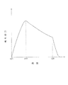
【解決手段】フラッシュランプの発光出力を1ミリ秒以上20ミリ秒以下の時間をかけて最大値にまで到達させる第1照射を行うことにより、不純物が注入された半導体ウェハーの表面温度を予備加熱温度T1から目標温度T2にまで1ミリ秒以上20ミリ秒以下にて昇温している。これにより不純物の活性化が達成される。続いて、フラッシュランプの発光出力を3ミリ秒以上50ミリ秒以下の時間をかけて最大値から徐々に低下させる第2照射を行うことにより、半導体ウェハーWの表面温度を目標温度T2から±25℃以内の範囲内に3ミリ秒以上50ミリ秒以下維持している。これにより、不純物の拡散を抑制しつつプロセスダメージの発生を防止することができる。
【選択図】図14
Description
2 シャッター機構
3 制御部
4 ハロゲン加熱部
5 フラッシュ加熱部
6 チャンバー
7 保持部
10 移載機構
21 シャッター板
22 スライド駆動機構
31 パルス発生器
32 波形設定部
33 入力部
61 チャンバー側部
62 凹部
63 上側チャンバー窓
64 下側チャンバー窓
65 熱処理空間
74 サセプター
91 トリガー電極
92 ガラス管
93 コンデンサ
94 コイル
96 IGBT
97 トリガー回路
FL フラッシュランプ
HL ハロゲンランプ
W 半導体ウェハー
Claims (8)
- 不純物が注入された基板に光を照射することによって該基板を加熱して不純物の活性化を行う熱処理方法であって、
基板を所定の予備加熱温度にて加熱する予備加熱工程と、
前記基板に光を照射することによって前記基板の表面温度を前記予備加熱温度から目標温度にまで1ミリ秒以上20ミリ秒以下にて昇温する昇温工程と、
前記昇温工程の後、前記基板に光を照射することによって前記基板の表面温度を前記目標温度から±25℃以内の範囲内に3ミリ秒以上50ミリ秒以下維持する温度維持工程と、
を備えることを特徴とする熱処理方法。 - 請求項1記載の熱処理方法において、
前記予備加熱温度は300℃以上800℃以下であり、
前記目標温度は1000℃以上1400℃以下であることを特徴とする熱処理方法。 - 請求項1または請求項2に記載の熱処理方法において、
前記昇温工程および前記温度維持工程では、フラッシュランプから前記基板にフラッシュ光を照射することを特徴とする熱処理方法。 - 請求項3記載の熱処理方法において、
前記昇温工程および前記温度維持工程では、コンデンサから前記フラッシュランプへの電荷の供給をスイッチング素子によって断続することにより前記フラッシュランプの発光出力を制御することを特徴とする熱処理方法。 - 不純物が注入された基板に光を照射することによって該基板を加熱して不純物の活性化を行う熱処理装置であって、
基板を収容するチャンバーと、
前記チャンバー内にて基板を保持する保持手段と、
前記保持手段に保持された基板を所定の予備加熱温度に加熱する予備加熱手段と、
前記保持手段に保持された基板に光を照射する光照射手段と、
前記光照射手段の発光出力を制御する発光制御手段と、
を備え、
前記発光制御手段は、前記保持手段に保持された基板に光を照射することによって前記基板の表面温度を前記予備加熱温度から目標温度にまで1ミリ秒以上20ミリ秒以下にて昇温した後、前記基板の表面温度を前記目標温度から±25℃以内の範囲内に3ミリ秒以上50ミリ秒以下維持するように前記光照射手段の発光出力を制御することを特徴とする熱処理装置。 - 請求項5記載の熱処理装置において、
前記予備加熱温度は300℃以上800℃以下であり、
前記目標温度は1000℃以上1400℃以下であることを特徴とする熱処理装置。 - 請求項5または請求項6に記載の熱処理装置において、
前記光照射手段は、フラッシュ光を照射するフラッシュランプを含むことを特徴とする熱処理装置。 - 請求項7記載の熱処理装置において、
前記発光制御手段は、コンデンサから前記フラッシュランプへの電荷の供給を断続することにより前記フラッシュランプの発光出力を制御するスイッチング素子を含むことを特徴とする熱処理装置。
Priority Applications (10)
| Application Number | Priority Date | Filing Date | Title |
|---|---|---|---|
| JP2011063735A JP2012199470A (ja) | 2011-03-23 | 2011-03-23 | 熱処理方法および熱処理装置 |
| TW101105891A TWI566300B (zh) | 2011-03-23 | 2012-02-22 | 熱處理方法及熱處理裝置 |
| KR1020120019495A KR101324860B1 (ko) | 2011-03-23 | 2012-02-27 | 열처리 방법 및 열처리 장치 |
| US13/417,498 US9343313B2 (en) | 2011-03-23 | 2012-03-12 | Heat treatment method and heat treatment apparatus for heating substrate by irradiating substrate with light |
| KR1020130044035A KR20130046415A (ko) | 2011-03-23 | 2013-04-22 | 열처리 방법 및 열처리 장치 |
| KR1020140030112A KR101788909B1 (ko) | 2011-03-23 | 2014-03-14 | 열처리 방법 및 열처리 장치 |
| US15/143,043 US9805932B2 (en) | 2011-03-23 | 2016-04-29 | Heat treatment method and heat treatment apparatus for heating substrate by irradiating substrate with light |
| US15/142,830 US10276385B2 (en) | 2011-03-23 | 2016-04-29 | Heat treatment method and heat treatment apparatus for heating substrate by irradiating substrate with light |
| KR1020170132192A KR101821528B1 (ko) | 2011-03-23 | 2017-10-12 | 열처리 방법 및 열처리 장치 |
| US16/298,260 US10879072B2 (en) | 2011-03-23 | 2019-03-11 | Heat treatment method and heat treatment apparatus for heating substrate by irradiating substrate with light |
Applications Claiming Priority (1)
| Application Number | Priority Date | Filing Date | Title |
|---|---|---|---|
| JP2011063735A JP2012199470A (ja) | 2011-03-23 | 2011-03-23 | 熱処理方法および熱処理装置 |
Publications (1)
| Publication Number | Publication Date |
|---|---|
| JP2012199470A true JP2012199470A (ja) | 2012-10-18 |
Family
ID=47181377
Family Applications (1)
| Application Number | Title | Priority Date | Filing Date |
|---|---|---|---|
| JP2011063735A Pending JP2012199470A (ja) | 2011-03-23 | 2011-03-23 | 熱処理方法および熱処理装置 |
Country Status (1)
| Country | Link |
|---|---|
| JP (1) | JP2012199470A (ja) |
Cited By (3)
| Publication number | Priority date | Publication date | Assignee | Title |
|---|---|---|---|---|
| JP2014143298A (ja) * | 2013-01-24 | 2014-08-07 | Dainippon Screen Mfg Co Ltd | 熱処理装置および熱処理方法 |
| JP2020009927A (ja) * | 2018-07-09 | 2020-01-16 | フェニックス電機株式会社 | 加熱用ledランプ、およびそれを備えるウエハ加熱ユニット |
| JP2021520631A (ja) * | 2018-04-06 | 2021-08-19 | バリアン・セミコンダクター・エクイップメント・アソシエイツ・インコーポレイテッド | プロセスチャンバウインドウを冷却するためのシステム及び装置 |
Citations (6)
| Publication number | Priority date | Publication date | Assignee | Title |
|---|---|---|---|---|
| JP2004063863A (ja) * | 2002-07-30 | 2004-02-26 | Matsushita Electric Ind Co Ltd | 半導体装置の製造方法 |
| US20070235662A1 (en) * | 2006-03-29 | 2007-10-11 | Taiwan Semiconductor Manufacturing Co., Ltd. | Flash lamp annealing device |
| JP2009070948A (ja) * | 2007-09-12 | 2009-04-02 | Dainippon Screen Mfg Co Ltd | 熱処理装置 |
| JP2009277759A (ja) * | 2008-05-13 | 2009-11-26 | Dainippon Screen Mfg Co Ltd | 熱処理方法および熱処理装置 |
| JP2010525581A (ja) * | 2007-05-01 | 2010-07-22 | マトソン テクノロジー カナダ インコーポレイテッド | 照射パルス熱処理方法および装置 |
| US20100210086A1 (en) * | 2009-02-19 | 2010-08-19 | Li-Ting Wang | Junction Profile Engineering Using Staged Thermal Annealing |
-
2011
- 2011-03-23 JP JP2011063735A patent/JP2012199470A/ja active Pending
Patent Citations (6)
| Publication number | Priority date | Publication date | Assignee | Title |
|---|---|---|---|---|
| JP2004063863A (ja) * | 2002-07-30 | 2004-02-26 | Matsushita Electric Ind Co Ltd | 半導体装置の製造方法 |
| US20070235662A1 (en) * | 2006-03-29 | 2007-10-11 | Taiwan Semiconductor Manufacturing Co., Ltd. | Flash lamp annealing device |
| JP2010525581A (ja) * | 2007-05-01 | 2010-07-22 | マトソン テクノロジー カナダ インコーポレイテッド | 照射パルス熱処理方法および装置 |
| JP2009070948A (ja) * | 2007-09-12 | 2009-04-02 | Dainippon Screen Mfg Co Ltd | 熱処理装置 |
| JP2009277759A (ja) * | 2008-05-13 | 2009-11-26 | Dainippon Screen Mfg Co Ltd | 熱処理方法および熱処理装置 |
| US20100210086A1 (en) * | 2009-02-19 | 2010-08-19 | Li-Ting Wang | Junction Profile Engineering Using Staged Thermal Annealing |
Cited By (6)
| Publication number | Priority date | Publication date | Assignee | Title |
|---|---|---|---|---|
| JP2014143298A (ja) * | 2013-01-24 | 2014-08-07 | Dainippon Screen Mfg Co Ltd | 熱処理装置および熱処理方法 |
| US9607870B2 (en) | 2013-01-24 | 2017-03-28 | SCREEN Holdings Co., Ltd. | Heat treatment apparatus and heat treatment method for heating substrate by irradiating substrate with flash of light |
| US9875919B2 (en) | 2013-01-24 | 2018-01-23 | SCREEN Holdings, Co. Ltd. | Heat treatment method for heating substrate by irradiating substrate with flash of light |
| JP2021520631A (ja) * | 2018-04-06 | 2021-08-19 | バリアン・セミコンダクター・エクイップメント・アソシエイツ・インコーポレイテッド | プロセスチャンバウインドウを冷却するためのシステム及び装置 |
| JP7144530B2 (ja) | 2018-04-06 | 2022-09-29 | バリアン・セミコンダクター・エクイップメント・アソシエイツ・インコーポレイテッド | プロセスチャンバウインドウを冷却するためのシステム及び装置 |
| JP2020009927A (ja) * | 2018-07-09 | 2020-01-16 | フェニックス電機株式会社 | 加熱用ledランプ、およびそれを備えるウエハ加熱ユニット |
Similar Documents
| Publication | Publication Date | Title |
|---|---|---|
| JP5951241B2 (ja) | 熱処理方法および熱処理装置 | |
| JP6560550B2 (ja) | 熱処理方法および熱処理装置 | |
| JP6539568B2 (ja) | 熱処理方法および熱処理装置 | |
| JP5507274B2 (ja) | 熱処理方法および熱処理装置 | |
| JP6184697B2 (ja) | 熱処理装置および熱処理方法 | |
| JP6026090B2 (ja) | 熱処理方法 | |
| JP5507227B2 (ja) | 熱処理方法および熱処理装置 | |
| JP6598630B2 (ja) | 熱処理方法 | |
| JP5731230B2 (ja) | 熱処理装置 | |
| JP6473659B2 (ja) | 熱処理方法および熱処理装置 | |
| JP5955670B2 (ja) | 熱処理方法 | |
| JP5944131B2 (ja) | 熱処理方法 | |
| JP5944152B2 (ja) | 熱処理方法および熱処理装置 | |
| JP2012199470A (ja) | 熱処理方法および熱処理装置 | |
| JP2018018873A (ja) | 熱処理方法 | |
| JP5797916B2 (ja) | 熱処理方法および熱処理装置 | |
| JP5698040B2 (ja) | 熱処理方法および熱処理装置 | |
| JP6005946B2 (ja) | 熱処理装置 | |
| JP7307563B2 (ja) | 熱処理方法および熱処理装置 | |
| JP5701651B2 (ja) | 熱処理方法および熱処理装置 | |
| JP5801575B2 (ja) | 熱処理方法および熱処理装置 | |
| JP5801574B2 (ja) | 熱処理方法および熱処理装置 | |
| JP2018029128A (ja) | ドーパント導入方法 | |
| JP2014049468A (ja) | 熱処理方法および熱処理装置 |
Legal Events
| Date | Code | Title | Description |
|---|---|---|---|
| A621 | Written request for application examination |
Free format text: JAPANESE INTERMEDIATE CODE: A621 Effective date: 20140303 |
|
| A977 | Report on retrieval |
Free format text: JAPANESE INTERMEDIATE CODE: A971007 Effective date: 20141031 |
|
| A131 | Notification of reasons for refusal |
Free format text: JAPANESE INTERMEDIATE CODE: A131 Effective date: 20141104 |
|
| A521 | Written amendment |
Free format text: JAPANESE INTERMEDIATE CODE: A523 Effective date: 20141224 |
|
| A131 | Notification of reasons for refusal |
Free format text: JAPANESE INTERMEDIATE CODE: A131 Effective date: 20150804 |
|
| A02 | Decision of refusal |
Free format text: JAPANESE INTERMEDIATE CODE: A02 Effective date: 20160322 |