JP2012201919A - Sputtering device and sputtering method - Google Patents
Sputtering device and sputtering method Download PDFInfo
- Publication number
- JP2012201919A JP2012201919A JP2011066668A JP2011066668A JP2012201919A JP 2012201919 A JP2012201919 A JP 2012201919A JP 2011066668 A JP2011066668 A JP 2011066668A JP 2011066668 A JP2011066668 A JP 2011066668A JP 2012201919 A JP2012201919 A JP 2012201919A
- Authority
- JP
- Japan
- Prior art keywords
- target
- axis
- sputtering apparatus
- magnetic field
- unit
- Prior art date
- Legal status (The legal status is an assumption and is not a legal conclusion. Google has not performed a legal analysis and makes no representation as to the accuracy of the status listed.)
- Withdrawn
Links
Images

Classifications
-
- C—CHEMISTRY; METALLURGY
- C23—COATING METALLIC MATERIAL; COATING MATERIAL WITH METALLIC MATERIAL; CHEMICAL SURFACE TREATMENT; DIFFUSION TREATMENT OF METALLIC MATERIAL; COATING BY VACUUM EVAPORATION, BY SPUTTERING, BY ION IMPLANTATION OR BY CHEMICAL VAPOUR DEPOSITION, IN GENERAL; INHIBITING CORROSION OF METALLIC MATERIAL OR INCRUSTATION IN GENERAL
- C23C—COATING METALLIC MATERIAL; COATING MATERIAL WITH METALLIC MATERIAL; SURFACE TREATMENT OF METALLIC MATERIAL BY DIFFUSION INTO THE SURFACE, BY CHEMICAL CONVERSION OR SUBSTITUTION; COATING BY VACUUM EVAPORATION, BY SPUTTERING, BY ION IMPLANTATION OR BY CHEMICAL VAPOUR DEPOSITION, IN GENERAL
- C23C14/00—Coating by vacuum evaporation, by sputtering or by ion implantation of the coating forming material
- C23C14/22—Coating by vacuum evaporation, by sputtering or by ion implantation of the coating forming material characterised by the process of coating
- C23C14/34—Sputtering
- C23C14/35—Sputtering by application of a magnetic field, e.g. magnetron sputtering
-
- C—CHEMISTRY; METALLURGY
- C23—COATING METALLIC MATERIAL; COATING MATERIAL WITH METALLIC MATERIAL; CHEMICAL SURFACE TREATMENT; DIFFUSION TREATMENT OF METALLIC MATERIAL; COATING BY VACUUM EVAPORATION, BY SPUTTERING, BY ION IMPLANTATION OR BY CHEMICAL VAPOUR DEPOSITION, IN GENERAL; INHIBITING CORROSION OF METALLIC MATERIAL OR INCRUSTATION IN GENERAL
- C23C—COATING METALLIC MATERIAL; COATING MATERIAL WITH METALLIC MATERIAL; SURFACE TREATMENT OF METALLIC MATERIAL BY DIFFUSION INTO THE SURFACE, BY CHEMICAL CONVERSION OR SUBSTITUTION; COATING BY VACUUM EVAPORATION, BY SPUTTERING, BY ION IMPLANTATION OR BY CHEMICAL VAPOUR DEPOSITION, IN GENERAL
- C23C14/00—Coating by vacuum evaporation, by sputtering or by ion implantation of the coating forming material
- C23C14/22—Coating by vacuum evaporation, by sputtering or by ion implantation of the coating forming material characterised by the process of coating
- C23C14/50—Substrate holders
- C23C14/505—Substrate holders for rotation of the substrates
-
- H—ELECTRICITY
- H01—ELECTRIC ELEMENTS
- H01J—ELECTRIC DISCHARGE TUBES OR DISCHARGE LAMPS
- H01J37/00—Discharge tubes with provision for introducing objects or material to be exposed to the discharge, e.g. for the purpose of examination or processing thereof
- H01J37/32—Gas-filled discharge tubes
- H01J37/34—Gas-filled discharge tubes operating with cathodic sputtering
- H01J37/3402—Gas-filled discharge tubes operating with cathodic sputtering using supplementary magnetic fields
- H01J37/3405—Magnetron sputtering
- H01J37/3408—Planar magnetron sputtering
-
- H—ELECTRICITY
- H01—ELECTRIC ELEMENTS
- H01J—ELECTRIC DISCHARGE TUBES OR DISCHARGE LAMPS
- H01J37/00—Discharge tubes with provision for introducing objects or material to be exposed to the discharge, e.g. for the purpose of examination or processing thereof
- H01J37/32—Gas-filled discharge tubes
- H01J37/34—Gas-filled discharge tubes operating with cathodic sputtering
- H01J37/3411—Constructional aspects of the reactor
- H01J37/345—Magnet arrangements in particular for cathodic sputtering apparatus
- H01J37/3455—Movable magnets
Landscapes
- Chemical & Material Sciences (AREA)
- Engineering & Computer Science (AREA)
- Physics & Mathematics (AREA)
- Plasma & Fusion (AREA)
- Analytical Chemistry (AREA)
- Chemical Kinetics & Catalysis (AREA)
- Materials Engineering (AREA)
- Mechanical Engineering (AREA)
- Metallurgy (AREA)
- Organic Chemistry (AREA)
- Physical Vapour Deposition (AREA)
- Electrodes Of Semiconductors (AREA)
Abstract
Description
本発明の実施形態は、スパッタ装置およびスパッタ方法に関する。 Embodiments described herein relate generally to a sputtering apparatus and a sputtering method.
従来、ウェハ基板の表面に薄膜を形成する装置として、スパッタ装置が知られている。かかるスパッタ装置では、装置内において不活性ガスのイオンを薄膜の材料となるターゲットへ衝突させ、衝突のエネルギーによりターゲットから放出される材料の原子をウェハ基板の表面へ堆積させることにより薄膜を形成する。 Conventionally, a sputtering apparatus is known as an apparatus for forming a thin film on the surface of a wafer substrate. In such a sputtering apparatus, an inert gas ion collides with a target, which is a material of the thin film, in the apparatus, and atoms of the material released from the target are deposited on the surface of the wafer substrate by the energy of the collision to form a thin film. .
また、スパッタ装置の一種として、ターゲットを介してウェハ基板と対向する位置に磁石を設け、かかる磁石によってターゲットへのイオンの衝突を促進させることにより成膜速度を高めたマグネトロン方式のスパッタ装置がある。 As one type of sputtering apparatus, there is a magnetron type sputtering apparatus in which a magnet is provided at a position facing a wafer substrate through a target, and the collision speed of ions to the target is promoted by such a magnet to increase the deposition rate. .
かかるマグネトロン方式のスパッタ装置では、磁石によって形成される磁界の強度にむらがあるため、イオンの衝突によって浸食されるターゲットの浸食速度は、ターゲットの部位によって異なる。 In such a magnetron type sputtering apparatus, since the intensity of the magnetic field formed by the magnet is uneven, the erosion speed of the target eroded by the collision of ions varies depending on the site of the target.
そして、ターゲットは、局所的に浸食された部位の浸食量が一定量に達した場合、利用可能な部位が残っている状態であっても交換が必要になる。このことから、マグネトロン方式のスパッタ装置では、ターゲットの利用効率を向上させる必要がある。 And when the amount of erosion of the part eroded locally reaches a certain amount, the target needs to be replaced even if the usable part remains. For this reason, in the magnetron type sputtering apparatus, it is necessary to improve the utilization efficiency of the target.
本発明が解決しようとする課題は、ターゲットの利用効率を向上させることができるスパッタ装置およびスパッタ方法を提供することである。 The problem to be solved by the present invention is to provide a sputtering apparatus and a sputtering method capable of improving the utilization efficiency of a target.
実施形態によれば、スパッタ装置が提供される。スパッタ装置は、底面がウェハ基板と対向配置可能なターゲットと、前記ターゲットの上面に対向配置され、磁界を形成する磁石を含んだ磁界形成部と、前記ターゲットと前記磁界形成部との間隔を維持させつつ、前記磁界形成部に前記ターゲットの前記ウェハ基板と対向する面における中心点の周りを周回させながら、当該中心点から前記磁界形成部における所定の基準点までの距離を変化させる機構と、前記ウェハ基板を所定の位置に配置可能なウェハ保持部とを備える。 According to the embodiment, a sputtering apparatus is provided. The sputtering apparatus maintains a gap between a target whose bottom surface can be arranged to face the wafer substrate, a magnetic field forming unit which is arranged to face the top surface of the target and includes a magnet for forming a magnetic field, and the target and the magnetic field forming unit. A mechanism for changing the distance from the center point to a predetermined reference point in the magnetic field forming unit while causing the magnetic field forming unit to circulate around a central point on the surface of the target facing the wafer substrate; A wafer holder that can place the wafer substrate at a predetermined position.
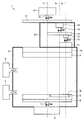
以下に、添付図面を参照して、第1〜3の実施形態にかかるスパッタ装置およびスパッタ方法を詳細に説明する。なお、これらの実施形態によって本発明が限定されるものではない。図1は、第1の実施形態にかかるスパッタ装置1を示す模式図である。 Hereinafter, a sputtering apparatus and a sputtering method according to first to third embodiments will be described in detail with reference to the accompanying drawings. Note that the present invention is not limited by these embodiments. FIG. 1 is a schematic diagram showing a sputtering apparatus 1 according to the first embodiment.
(第1の実施形態)
図1に示すように、スパッタ装置1は、処理チャンバ2と、真空制御部3と、ガス供給部4とを備えている。処理チャンバ2は、たとえば、シリコンウェハなどのウェハ基板Wに対してスパッタリング処理を行う処理室である。
(First embodiment)
As shown in FIG. 1, the sputtering apparatus 1 includes a
真空制御部3は、処理チャンバ2の内部から空気を吸引することによって処理チャンバ2内を減圧する真空ポンプである。ガス供給部4は、プラズマ発生用の不活性ガス(たとえば、アルゴンガス)を処理チャンバ2の内部へ導入する処理部である。
The
また、スパッタ装置1は、処理チャンバ2の内部に処理対象のウェハ基板Wを保持するウェハ保持部(以下、「ペデスタル6」と記載する)を備える。ペデスタル6は、ウェハ基板Wが所定位置にセットされたシールド5を保持する。また、スパッタ装置1は、基板駆動ユニット8を備える。基板駆動ユニット8は、回転シャフト7を、回転軸Cを中心に回転させることでペデスタル6を回転させる。
Further, the sputtering apparatus 1 includes a wafer holding unit (hereinafter referred to as “
また、スパッタ装置1は、ウェハ基板Wの上面に対して底面を平行に対向配置可能なターゲット9と、ターゲット9を処理チャンバ2内部で保持するバックプレート10とを備える。
In addition, the sputtering apparatus 1 includes a
ターゲット9は、円盤状であり、ウェハ基板Wの表面に成膜する薄膜の材料となる部材である。また、バックプレート10は、ターゲット9と径が同じ円盤状の部材である。なお、かかるターゲット9およびバックプレート10の径や形状はこれに限るものではない。
The
ここで、かかるスパッタ装置1による薄膜の成膜手順について簡単に説明する。スパッタ装置1は、まず、真空制御部3によって処理チャンバ2の内部を所定の気圧まで減圧させる。続いて、スパッタ装置1は、ガス供給部4によって処理チャンバ2内へ不活性ガスを導入させる。
Here, a procedure for forming a thin film by the sputtering apparatus 1 will be briefly described. First, the sputtering apparatus 1 depressurizes the inside of the
続いて、スパッタ装置1は、ターゲット9とペデスタル6との間に所定の電圧を印加することによって不活性ガスをプラズマ化させ、プラズマ化したイオンをターゲット9の底面へ衝突させる。かかるイオンの衝突によってターゲット9の原子がターゲット9から弾き出される。そして、スパッタ装置1は、ターゲット9から弾き出された原子をウェハ基板Wの表面へ堆積させることによってウェハ基板Wの表面にターゲット9の原子からなる薄膜を成膜する。
Subsequently, the sputtering apparatus 1 converts the inert gas into plasma by applying a predetermined voltage between the
また、スパッタ装置1は、バックプレート10を介してターゲット9と対向する位置にマグネトロン装置20を備える。かかるマグネトロン装置20は、ターゲット9の底面に磁界を形成する装置である。そして、スパッタ装置1では、マグネトロン装置20によって磁界を形成することでターゲット9へ衝突するイオンの密度を高めることにより成膜速度を高めている。
Further, the sputtering apparatus 1 includes a
かかるマグネトロン装置20は、1個以上の磁石が固定された磁界形成部(以下、「マグネット部11」と記載する)と、マグネット駆動ユニット13と、ユニット支持板14と、支持板駆動ユニット16とを備える。
The
マグネット部11は、円盤状の部材であり、バックプレート10を介してターゲット9と対向する位置に配置され、ターゲット9の底面に磁界を形成する。かかるマグネット部11は、上面の中心に立設された回転シャフト12によってマグネット駆動ユニット13に連結される。なお、かかるマグネット部11の径や形状はこれに限るものではない。
The
マグネット駆動ユニット13は、第1軸である軸Aを中心に回転シャフト12を回転させることにより、マグネット部11の底面とターゲット9の底面とを平行に保ちつつ、軸Aを回転軸としてマグネット部11を自転させる。かかるマグネット駆動ユニット13は、ユニット支持板14によって支持される。
The
ユニット支持板14は、円盤状の支持部材であり、下面の所定位置に取り付けられるマグネット駆動ユニット13を支持する。かかるユニット支持板14は、上面の中心に立設された回転シャフト15によって支持板駆動ユニット16に連結される。
The
支持板駆動ユニット16は、第2軸である軸Bを中心に回転シャフト15を回転させることにより、ユニット支持板14の底面とターゲット9の底面とを平行に保ちつつ、軸Bを回転軸としてユニット支持板14を自転させる。
The support
また、スパッタ装置1は、マグネトロン装置20を支持する装置支持板17と、装置支持板17を駆動する装置駆動ユニット19とを備える。装置支持板17は、円盤状の支持部材であり、下面の所定位置に取り付けられる支持板駆動ユニット16を支持する。かかる装置支持板17は、上面の中心に立設された回転シャフト18によって装置駆動ユニット19に連結される。
Further, the sputtering apparatus 1 includes a
装置駆動ユニット19は、第3軸である軸Cを中心に回転シャフト18を回転させることにより、装置支持板17の底面とターゲット9の底面とを平行に保ちつつ、軸Cを回転軸として装置支持板17を自転させる。
The
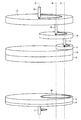
次に、図2を用いてスパッタ装置1の各駆動ユニットによって駆動される部材の形状、配置および動作について説明する。図2は、第1の実施形態にかかるスパッタ装置1の各駆動ユニットによって駆動される部材の形状、配置および動作を示す図である。なお、図2では、各駆動ユニットの図示を省略している。 Next, the shape, arrangement, and operation of the members driven by each drive unit of the sputtering apparatus 1 will be described with reference to FIG. FIG. 2 is a diagram illustrating the shape, arrangement, and operation of members driven by each drive unit of the sputtering apparatus 1 according to the first embodiment. In addition, illustration of each drive unit is abbreviate | omitted in FIG.
図2に示すように、スパッタ装置1では、ペデスタル6、シールド5、ターゲット9、バックプレート10および装置支持板17は、いずれも径が等しい。なお、かかる径は一例に過ぎず、各部の径は変更できる。
As shown in FIG. 2, in the sputtering apparatus 1, the
また、スパッタ装置1では、ペデスタル6、シールド5、ターゲット9、バックプレート10および装置支持板17は、軸C上に各上下面の中心が位置するように配置される。さらに、ペデスタル6を回転する回転シャフト7および装置支持板17を回転する回転シャフト18は、軸Cを回転軸として回転するように配置される。
In the sputtering apparatus 1, the
シールド5は、上面の中心と外周との間に、円盤状のウェハ基板Wを嵌合可能な嵌合穴を備え、かかる嵌合穴内でウェハ基板Wを保持する。
The
ユニット支持板14は、直径がターゲット9の半径と等しくなるように形成される。なお、かかる径は一例に過ぎない。そして、ユニット支持板14は、ターゲット9における底面の中心とターゲット9の外周との中点を通り、軸Cに平行な軸Bを回転軸として回転する位置に配置される。
The
マグネット部11は、直径がユニット支持板14の半径と等しい。なお、かかる径は一例に過ぎない。そして、マグネット部11は、ユニット支持板14における底面の中心とユニット支持板14の外周との中点を通り、軸Bに平行な軸Aを回転軸として回転する位置に配置される。
The
そして、スパッタ装置1では、マグネット部11、ユニット支持板14、装置支持板17、およびペデスタル6を同時に回転させる。このとき、スパッタ装置1では、マグネット部11の回転速度よりも遅い回転速度でユニット支持板14を回転させ、ユニット支持板14の回転速度よりも遅い回転速度で装置支持板17を回転させる。
In the sputtering apparatus 1, the
すなわち、スパッタ装置1では、マグネット部11、ユニット支持板14、装置支持板17、およびペデスタル6を同時に回転させることで、マグネット部11が、ターゲット9との距離を維持しつつ軸Aを回転軸として自転しながら軸Bの周りを公転し、さらに、軸Cの周りを公転する。
That is, in the sputtering apparatus 1, the
このように、スパッタ装置1では、マグネット部11に連動連結される回転シャフト12、マグネット駆動ユニット13、ユニット支持板14、回転シャフト15、支持板駆動ユニット16、装置支持板17、回転シャフト18および装置駆動ユニット19を含む機構により、上記のようにターゲット9の上方でマグネット部11を移動させる。
Thus, in the sputtering apparatus 1, the
これにより、スパッタ装置1では、ターゲット9とマグネット部11との間隔を維持させつつ、ターゲット9のウェハ基板Wと対向する面における中心点からマグネット部11における所定の基準点(たとえば、マグネット部11における下面の中心点)までの距離を変化させることができる。したがって、スパッタ装置1は、ターゲット9との距離を維持させつつ、バックプレート10の上面と面する全領域を網羅するようにマグネット部11を移動させることができる。
Thereby, in the sputtering apparatus 1, while maintaining the distance between the
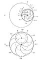
ここで、図3を用いてターゲット9の底面に対するマグネット部11の移動範囲について説明する。図3は、第1の実施形態にかかるターゲット9の底面に対するマグネット部11の移動範囲を示す図である。
Here, the moving range of the
なお、図3(a)には、支持板駆動ユニット16によって移動するマグネット部11の移動範囲を示しており、図3(b)には、装置駆動ユニット19によって移動するマグネット部11の移動範囲を示している。また、図3(a)では、説明を簡略化する観点から軸Bを固定した場合におけるマグネット部11の移動範囲を示している。
3A shows the moving range of the
図3(a)に示すように、スパッタ装置1では、軸Aを回転軸としてマグネット部11を自転させながら(図3(a)における点線矢印参照)、支持板駆動ユニット16により軸Bを回転軸としてユニット支持板14を自転させる。
As shown in FIG. 3A, in the sputtering apparatus 1, the shaft B is rotated by the support
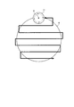
その結果、マグネット部11は、位置11−1、11−2、11−3、11−4、11−5、11−6、11−7、11−8の順に移動しながら軸Bの周りを公転して位置11−1へ戻る。
As a result, the
これにより、スパッタ装置1では、ターゲット9の底面におけるユニット支持板14と重なり合う全領域を網羅するようにターゲット9の上方でマグネット部11を移動させることができる。
Thereby, in the sputtering apparatus 1, the
さらに、スパッタ装置1では、図3(b)に示すように、軸Bを回転軸としてユニット支持板14を自転させながら(図3(b)における一点鎖線矢印参照)、装置駆動ユニット19によって軸Cを回転軸として装置支持板17を自転させる。
Further, in the sputtering apparatus 1, as shown in FIG. 3B, while rotating the
その結果、ユニット支持板14は、位置14−1、14−2、14−3、14−4、14−5、14−6、14−7、14−8の順に移動しながら軸Cの周りを公転して位置14−1へ戻る。
As a result, the
このように、スパッタ装置1では、ターゲット9における底面の全領域を網羅するようにターゲット9の上方でユニット支持板14を移動させる。そして、前述したように、マグネット部11は、ターゲット9の底面におけるユニット支持板14と重なり合う全領域を網羅するようにターゲット9の上方を移動する。
As described above, in the sputtering apparatus 1, the
したがって、スパッタ装置1では、ターゲット9の底面全体を網羅するようにターゲット9の上方でマグネット部11を移動させることが可能となり、イオンが高密度に衝突する領域をターゲット9の底面における全領域にわたって移動させることができる。
Therefore, in the sputtering apparatus 1, it is possible to move the
これにより、スパッタ装置1は、ターゲット9の底面全体に対して均一にイオンを衝突させて底面全体を均一に浸食させることによりターゲット9の利用効率を向上させることができる。
Thereby, the sputtering apparatus 1 can improve the utilization efficiency of the
さらに、スパッタ装置1では、ターゲット9から放出された原子がターゲット9の底面へ再付着した場合であっても、原子が再付着した部位へ高密度にイオンが衝突する期間が一定周期で訪れる。これにより、スパッタ装置1では、ターゲット9の底面に再付着した原子を定期的に除去されるので、成膜する薄膜上にパーティクルが生じることを防止することができる。
Furthermore, in the sputtering apparatus 1, even when atoms emitted from the
図2の説明に戻り、各駆動ユニットによって駆動される部材の配置および動作の説明を続ける。スパッタ装置1では、ペデスタル6は、ウェハ基板Wの中心と第2軸である軸Bとが一致するように、ウェハ基板Wを配置可能に構成される。
Returning to the description of FIG. 2, the description of the arrangement and operation of the members driven by the drive units will be continued. In the sputtering apparatus 1, the
具体的には、スパッタ装置1は、基板駆動ユニット8によるペデスタル6の回転速度と、装置駆動ユニット19による装置支持板17の回転速度とが等しくなるようにペデスタル6および装置支持板17の回転を制御する。
Specifically, the sputtering apparatus 1 rotates the
さらに、スパッタ装置1は、ユニット支持板14を回転する回転シャフト15の回転軸となる軸Bの延長線上にウェハ基板W表面の中心点が常に位置するようペデスタル6および装置支持板17の回転を制御する。
Further, the sputtering apparatus 1 rotates the
すなわち、スパッタ装置1は、平面視における面積の等しいウェハ基板Wおよびユニット支持板14が常に対向した状態を維持させる。そして、前述したように、スパッタ装置1は、ターゲット9の底面におけるユニット支持板14と重なり合う全領域を網羅するようにターゲット9の上方でマグネット部11を移動させる。
That is, the sputtering apparatus 1 always maintains a state where the wafer substrate W and the
これにより、スパッタ装置1では、ターゲット9の底面におけるウェハ基板Wと面する領域からウェハ基板Wの表面へターゲット9の原子を均等に堆積させることが可能となり、均等な膜厚の薄膜を成膜することができる。
As a result, in the sputtering apparatus 1, atoms of the
上述したように、第1の実施形態にかかるスパッタ装置1は、底面がウェハ基板Wの上面に対向配置されたターゲット9と、ターゲット9の上面に対向配置され、磁界を形成する磁石を含んだマグネット部11と、ターゲット9とマグネット部11との間隔を維持させつつ、ターゲット9のウェハ基板Wと対向する面における中心点からマグネット部11における所定の基準点までの距離を変化させる機構とを備える。
As described above, the sputtering apparatus 1 according to the first embodiment includes the
かかる構成により、スパッタ装置1は、ターゲット9の底面全体を網羅するようにターゲット9の上方でマグネット部11を移動させることができる。これにより、スパッタ装置1は、ターゲット9の底面全体に対して均一にイオンを衝突させて、ターゲット9の底面全体を均一に浸食させることによりターゲット9の利用効率を向上させることができる。
With this configuration, the sputtering apparatus 1 can move the
また、スパッタ装置1は、マグネット部11にターゲット9のウェハ基板Wと対向する面における中心点の周りを周回させながら、ターゲット9のウェハ基板Wと対向する面における中心点からマグネット部11における所定の基準点までの距離を変化させる。
Further, the sputtering apparatus 1 causes the
これにより、スパッタ装置1は、ターゲット9における底面の各部位へ周期的に高密度なイオンを衝突させることができるため、ターゲット9の底面へ再付着した原子を周期的に除去することで成膜する薄膜にパーティクルが生じることを防止することができる。
Thereby, since the sputtering apparatus 1 can periodically collide high-density ions with each part of the bottom surface of the
また、スパッタ装置1は、第1軸となるA軸を回転軸としてマグネット部11をターゲット9の上面に沿って回転させる第1回転機構(マグネット駆動ユニット13)と、第2軸となるB軸を回転軸として第1軸をターゲット9の上面に沿って回転させる第2回転機構(支持板駆動ユニット16)とを備える。
The sputtering apparatus 1 includes a first rotation mechanism (magnet drive unit 13) that rotates the
さらに、スパッタ装置1は、ターゲット9のウェハ基板Wと対向する面における中心点を通り第2軸に対して平行な第3軸となるC軸を回転軸として第2軸をターゲット9の上面に沿って回転する第3回転機構(装置駆動ユニット19)とを備える。
Further, the sputtering apparatus 1 uses the second axis as the upper surface of the
かかる構成により、スパッタ装置1は、マグネット部11の自転および公転の組み合わせによってターゲット9の底面と対向する任意の位置へマグネット部11を移動させることができる。
With this configuration, the sputtering apparatus 1 can move the
したがって、スパッタ装置1によれば、ターゲット9の底面から定常的にイオンの衝突頻度が低い領域を排除することができるため、ターゲット9の底面全体を均一に浸食させることによりターゲット9の利用効率を向上させることができる。
Therefore, according to the sputtering apparatus 1, since the region where the ion collision frequency is steadily low from the bottom surface of the
(第2の実施形態)
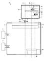
次に、図4を用いて第2の実施形態にかかるスパッタ装置1aについて説明する。図4は、第2の実施形態にかかるスパッタ装置1aを示す模式図である。なお、図4では、図1に示すスパッタ装置1と同様の構成要素に対して同一の符号を付している。
(Second Embodiment)
Next, a
図4に示すように、スパッタ装置1aは、マグネトロン装置20を固定した点、ターゲット駆動ユニット101を設けた点およびペデスタル60を固定した点が図1に示すスパッタ装置1と異なる。
As shown in FIG. 4, the
すなわち、スパッタ装置1aにおけるウェハ基板W、ターゲット9、バックプレート10、マグネット部11、回転シャフト12、マグネット駆動ユニット13、ユニット支持板14、回転シャフト15および支持板駆動ユニット16の形状および配置は、図1に示すものと同一である。また、図4に示す軸A、BおよびCの相対位置も図1に示すものと同一である。
That is, the shape and arrangement of the wafer substrate W, the
かかるスパッタ装置1aのターゲット駆動ユニット101は、バックプレート10の上面の中心に立設された回転シャフト100を駆動することにより、軸Cを回転軸としてバックプレート10およびターゲット9を回転させる。
The
ここで、図5を用いてスパッタ装置1aの各駆動ユニットによって駆動される部材の動作について説明する。図5は、第2の実施形態にかかるスパッタ装置1aの各駆動ユニットによって駆動される部材の動作を示す図である。
Here, the operation of the member driven by each drive unit of the
図5に示すように、スパッタ装置1aでは、マグネット部11は、軸Aを回転軸として自転しながら、ウェハ基板W表面の中心点を通る軸Bの周りを公転する。これにより、マグネット部11は、ターゲット9の底面におけるユニット支持板14と重なり合う全領域を網羅するようにターゲット9の上方を移動する。
As shown in FIG. 5, in the
そして、ターゲット9は、ターゲット駆動ユニット101によって回転シャフト100が回転駆動されると、ユニット支持板14と重なり合う領域をずらしながら軸Cを回転軸として自転する。
Then, when the
かかる動作によっても、スパッタ装置1aは、ターゲット9とマグネット部11との間隔を維持させつつ、ターゲット9のウェハ基板Wと対向する面における中心点からマグネット部11における所定の基準点までの距離を変化させることができる。
Also by such an operation, the
このように、第2の実施形態にかかるスパッタ装置1aは、第1軸となるA軸を回転軸としてマグネット部11をターゲット9の上面に沿って回転させる第1回転機構(マグネット駆動ユニット13)と、第2軸となるB軸を回転軸として第1軸をターゲット9の上面に沿って回転させる第2回転機構(支持板駆動ユニット16)とを備える。
As described above, the
さらに、スパッタ装置1aは、ターゲット9のウェハ基板Wと対向する面における中心点を通り第2軸に対して平行な第3軸となるC軸を回転軸としてターゲット9を回転する第3回転機構(ターゲット駆動ユニット101)を備える。
Further, the
かかる構成により、スパッタ装置1aは、マグネット部11の自転、公転およびターゲット9の自転の組み合わせによって、ターゲット9の底面の全領域を網羅するようにマグネット部11を移動させることができる。
With such a configuration, the
したがって、スパッタ装置1aは、図1に示したスパッタ装置1と同様に、ターゲット9の底面全体を均一に浸食させることでターゲット9の利用効率を向上させることができる。また、スパッタ装置1aは、図1に示したスパッタ装置1と同様に、ターゲット9の底面に再付着した原子を周期的に除去することができる。
Therefore, the
なお、上記した実施形態では、マグネット部11の移動領域の面積と、ターゲット9の底面積とが等しい場合について説明したが、マグネット部11の移動領域の面積をターゲット9の底面積よりも広くしてもよい。
In the above-described embodiment, the case where the area of the moving region of the
かかる場合、マグネット部11の上面に立設された回転シャフト12がユニット支持板14の底面における中心よりも外周に近い位置となるようにマグネット駆動ユニット13を取り付ける。
In such a case, the
また、第1の実施形態のスパッタ装置1の場合には、ユニット支持板14の上面に立設された回転シャフト15が装置支持板17の底面における中心よりも外周に近い位置となるように、支持板駆動ユニット16を取り付けてもよい。
Further, in the case of the sputtering apparatus 1 of the first embodiment, the
これにより、スパッタ装置1および1aでは、ターゲット9の底面における周縁部までを確実に網羅するようにマグネット部11をターゲット9の上方で移動させることができる。
Thereby, in the
なお、上述した実施形態では、マグネット部11の自転および公転の軌道が全て円軌道の場合について説明したが、マグネット部11の自転および公転の軌道は楕円軌道など、円軌道以外の任意の軌道としてもよい。
In the above-described embodiment, the case where the rotation and revolution trajectories of the
また、上述した実施形態では、マグネット部11がターゲット9のウェハ基板Wと対向する面における中心点の周りを周回移動する場合について説明したが、マグネット部11をターゲット9の上方で往復移動させてもよい。
In the above-described embodiment, the case where the
(第3の実施形態)
次に、図6を用いてマグネット部11をターゲット9の上方で往復移動させる第3の実施形態のスパッタ装置について説明する。図6は、第3の実施形態にかかるスパッタ装置によって移動させるマグネット部11の移動軌跡を示す図である。
(Third embodiment)
Next, a sputtering apparatus according to a third embodiment in which the
図6に示すように、第3の実施形態に係るスパッタ装置は、軸Aを回転軸としてマグネット部11を自転させつつ、ターゲット9の底面とマグネット部11との距離を一定に保ちながらターゲット9の上方を走査するように蛇行させてマグネット部11を往復移動させる。
As shown in FIG. 6, the sputtering apparatus according to the third embodiment rotates the
この場合、スパッタ装置は、ターゲット9の底面に対して平行に第1の方向へマグネット部11を移動させる機構と、ターゲット9の底面に対して平行に第1の方向と直交する第2の方向へマグネット部11を移動させる機構とを備える。
In this case, the sputtering apparatus includes a mechanism that moves the
かかる構成によっても、スパッタ装置は、ターゲット9の底面と対向する任意の位置へマグネット部11を移動させることが可能なため、ターゲット9の底面全体を均一に浸食させることでターゲット9の利用効率を向上させることができる。
Even with such a configuration, the sputtering apparatus can move the
なお、上記した第1〜第3の実施形態では、薄膜の成膜中にターゲット9とユニット支持板14との相対位置を常時変化させる場合について説明したが、ターゲット9とユニット支持板14との相対位置を所定期間固定とし、周期的に変化させてもよい。
In the first to third embodiments described above, the case where the relative position between the
たとえば、所定の成膜工程を行っている間、ターゲット9とユニット支持板14との相対位置を所定期間固定とし、工程が切り替わった場合に、ターゲット9とユニット支持板14との相対位置を変化させてもよい。
For example, while performing a predetermined film forming process, the relative position between the
また、予め定めた所定時間が経過するまでターゲット9とユニット支持板14との相対位置を固定とし、所定時間が経過した場合に、ターゲット9とユニット支持板14との相対位置を変化させてもよい。かかる構成によっても、ターゲット9とユニット支持板14との相対位置の変化を繰り返すことで、ターゲット9の底面全体を均一に浸食させることができる。
Further, the relative position between the
また、第1〜第3の実施形態では、マグネット部11を自転させる場合について説明したが、マグネット部11を自転させずに、ターゲット9とユニット支持板14との相対位置を変化させても、ターゲット9の底面全体を均一に浸食させることが可能である。
Moreover, although the case where the
また、第1の実施形態に記載した技術と、第2の実施形態に記載した技術とを組み合わせ、軸Cを自転軸としてターゲット9を自転させつつ、軸Cを公転軸としてユニット支持板14を公転させるようにスパッタ装置を構成してもよい。かかる構成によっても、ターゲット9の底面全体を均一に浸食させることができる。
Further, the technique described in the first embodiment and the technique described in the second embodiment are combined, and the
本発明のいくつかの実施形態を説明したが、これらの実施形態は、例として提示したものであり、発明の範囲を限定することは意図していない。これら新規な実施形態は、その他の様々な形態で実施されることが可能であり、発明の要旨を逸脱しない範囲で、種々の省略、置き換え、変更を行うことができる。これら実施形態やその変形は、発明の範囲や要旨に含まれるとともに、特許請求の範囲に記載された発明とその均等の範囲に含まれる。 Although several embodiments of the present invention have been described, these embodiments are presented by way of example and are not intended to limit the scope of the invention. These novel embodiments can be implemented in various other forms, and various omissions, replacements, and changes can be made without departing from the scope of the invention. These embodiments and modifications thereof are included in the scope and gist of the invention, and are included in the invention described in the claims and the equivalents thereof.
1、1a スパッタ装置、2 処理チャンバ、3 真空制御部、4 ガス供給部、5 シールド、6 ペデスタル、8 基板駆動ユニット、9 ターゲット、10 バックプレート、11 マグネット部、13 マグネット駆動ユニット、14 ユニット支持板、16 支持板駆動ユニット、17 装置支持板、19 装置駆動ユニット、20 マグネトロン装置、101 ターゲット駆動ユニット、7、12、15、18、100 回転シャフト 1, 1a Sputter device, 2 processing chamber, 3 vacuum control unit, 4 gas supply unit, 5 shield, 6 pedestal, 8 substrate drive unit, 9 target, 10 back plate, 11 magnet unit, 13 magnet drive unit, 14 unit support Plate, 16 support plate drive unit, 17 device support plate, 19 device drive unit, 20 magnetron device, 101 target drive unit, 7, 12, 15, 18, 100 rotary shaft
Claims (5)
前記ターゲットの上面に対向配置され、磁界を形成する磁石を含んだ磁界形成部と、
前記ターゲットと前記磁界形成部との間隔を維持させつつ、前記磁界形成部に前記ターゲットの前記ウェハ基板と対向する面における中心点の周りを周回させながら、当該中心点から前記磁界形成部における所定の基準点までの距離を変化させる機構と、
前記ウェハ基板を所定の位置に配置可能なウェハ保持部と
を備えたことを特徴とするスパッタ装置。 A target whose bottom can be placed opposite to the wafer substrate;
A magnetic field forming unit including a magnet that is disposed opposite to the upper surface of the target and forms a magnetic field;
While maintaining the distance between the target and the magnetic field forming part, the magnetic field forming part is rotated around the center point on the surface of the target facing the wafer substrate, and from the center point to the predetermined in the magnetic field forming part. A mechanism to change the distance to the reference point of
A sputtering apparatus comprising: a wafer holding unit capable of arranging the wafer substrate at a predetermined position.
第1軸を回転軸として前記磁界形成部を前記ターゲットの上面に沿って回転させる第1回転機構と、
第2軸を回転軸として前記第1軸を前記ターゲットの上面に沿って回転させる第2回転機構と、
前記中心点を通り前記第2軸に対して平行な第3軸を回転軸として前記第2軸を前記ターゲットの上面に沿って回転する第3回転機構と
を備えたことを特徴とする請求項1に記載のスパッタ装置。 The mechanism is
A first rotation mechanism for rotating the magnetic field forming unit along the upper surface of the target with a first axis as a rotation axis;
A second rotation mechanism for rotating the first axis along the upper surface of the target with a second axis as a rotation axis;
A third rotation mechanism that rotates the second axis along the upper surface of the target with a third axis passing through the center point and parallel to the second axis as a rotation axis. 2. The sputtering apparatus according to 1.
第1軸を回転軸として前記磁界形成部を前記ターゲットの上面に沿って回転させる第1回転機構と、
第2軸を回転軸として前記第1軸を前記ターゲットの上面に沿って回転させる第2回転機構と
前記中心点を通り前記第2軸に対して平行な第3軸を回転軸として前記ターゲットを回転する第3回転機構と
を備えたことを特徴とする請求項1または請求項2に記載のスパッタ装置。 The mechanism is
A first rotation mechanism for rotating the magnetic field forming unit along the upper surface of the target with a first axis as a rotation axis;
A second rotation mechanism that rotates the first axis along the upper surface of the target with a second axis as a rotation axis; and a third axis that passes through the center point and is parallel to the second axis. The sputtering apparatus according to claim 1, further comprising: a third rotating mechanism that rotates.
前記ウェハ基板の中心と前記第2軸とが一致するように、前記ウェハ基板を配置可能とする
ことを特徴とする請求項2または請求項3に記載のスパッタ装置。 The wafer holder is
The sputtering apparatus according to claim 2, wherein the wafer substrate can be arranged so that a center of the wafer substrate and the second axis coincide with each other.
磁界を形成する磁石を含んだ磁界形成部を前記ターゲットの上面に対向配置する工程と、
前記ターゲットと前記磁界形成部との間隔を維持させつつ、前記磁界形成部に前記ターゲットの前記ウェハ基板と対向する面における中心点の周りを周回させながら、当該中心点から前記磁界形成部における所定の基準点までの距離を変化させ成膜処理を行う工程と
を含んだことを特徴とするスパッタ方法。 A step of placing the bottom surface of the target opposite to the wafer substrate;
A step of disposing a magnetic field forming portion including a magnet for forming a magnetic field on the upper surface of the target;
While maintaining the distance between the target and the magnetic field forming part, the magnetic field forming part is rotated around the center point on the surface of the target facing the wafer substrate, and from the center point to the predetermined in the magnetic field forming part. And a film forming process by changing the distance to the reference point.
Priority Applications (2)
| Application Number | Priority Date | Filing Date | Title |
|---|---|---|---|
| JP2011066668A JP2012201919A (en) | 2011-03-24 | 2011-03-24 | Sputtering device and sputtering method |
| US13/354,670 US20120241311A1 (en) | 2011-03-24 | 2012-01-20 | Sputtering device and sputtering method |
Applications Claiming Priority (1)
| Application Number | Priority Date | Filing Date | Title |
|---|---|---|---|
| JP2011066668A JP2012201919A (en) | 2011-03-24 | 2011-03-24 | Sputtering device and sputtering method |
Publications (1)
| Publication Number | Publication Date |
|---|---|
| JP2012201919A true JP2012201919A (en) | 2012-10-22 |
Family
ID=46876399
Family Applications (1)
| Application Number | Title | Priority Date | Filing Date |
|---|---|---|---|
| JP2011066668A Withdrawn JP2012201919A (en) | 2011-03-24 | 2011-03-24 | Sputtering device and sputtering method |
Country Status (2)
| Country | Link |
|---|---|
| US (1) | US20120241311A1 (en) |
| JP (1) | JP2012201919A (en) |
Cited By (2)
| Publication number | Priority date | Publication date | Assignee | Title |
|---|---|---|---|---|
| JP2016517469A (en) * | 2013-03-05 | 2016-06-16 | アプライド マテリアルズ インコーポレイテッドApplied Materials,Incorporated | Sputter source for use in a semiconductor process chamber |
| JP2023533696A (en) * | 2020-06-30 | 2023-08-04 | アプライド マテリアルズ インコーポレイテッド | Multi-radius magnetron for physical vapor deposition (PVD) and method of use |
Families Citing this family (2)
| Publication number | Priority date | Publication date | Assignee | Title |
|---|---|---|---|---|
| JP5873311B2 (en) * | 2011-11-29 | 2016-03-01 | 太陽誘電株式会社 | Elastic wave device and multilayer substrate |
| CN115679277A (en) * | 2021-07-23 | 2023-02-03 | 北京北方华创微电子装备有限公司 | Reaction chamber and semiconductor processing equipment |
Family Cites Families (3)
| Publication number | Priority date | Publication date | Assignee | Title |
|---|---|---|---|---|
| JP2746695B2 (en) * | 1989-10-20 | 1998-05-06 | 東京エレクトロン株式会社 | Sputtering apparatus and sputtering method |
| US6841050B2 (en) * | 2002-05-21 | 2005-01-11 | Applied Materials, Inc. | Small planetary magnetron |
| JP2005187830A (en) * | 2003-12-24 | 2005-07-14 | Cyg Gijutsu Kenkyusho Kk | Sputtering apparatus |
-
2011
- 2011-03-24 JP JP2011066668A patent/JP2012201919A/en not_active Withdrawn
-
2012
- 2012-01-20 US US13/354,670 patent/US20120241311A1/en not_active Abandoned
Cited By (3)
| Publication number | Priority date | Publication date | Assignee | Title |
|---|---|---|---|---|
| JP2016517469A (en) * | 2013-03-05 | 2016-06-16 | アプライド マテリアルズ インコーポレイテッドApplied Materials,Incorporated | Sputter source for use in a semiconductor process chamber |
| JP2023533696A (en) * | 2020-06-30 | 2023-08-04 | アプライド マテリアルズ インコーポレイテッド | Multi-radius magnetron for physical vapor deposition (PVD) and method of use |
| JP7684334B2 (en) | 2020-06-30 | 2025-05-27 | アプライド マテリアルズ インコーポレイテッド | Multi-radius magnetron for physical vapor deposition (PVD) and method of use thereof - Patents.com |
Also Published As
| Publication number | Publication date |
|---|---|
| US20120241311A1 (en) | 2012-09-27 |
Similar Documents
| Publication | Publication Date | Title |
|---|---|---|
| KR102410186B1 (en) | Film forming apparatus and film forming substsrate manufacturing method | |
| JP7575866B2 (en) | Apparatus for controlling thickness variations in layers of material formed using physical vapor deposition - Patents.com | |
| CN111826624A (en) | HIPIMS sputtering method and HIPIMS sputtering system | |
| KR20170131816A (en) | Film forming apparatus and method for manufacturing a work film is formed | |
| JP2004156122A (en) | Film deposition method, and sputtering system | |
| JP6701455B2 (en) | Sputtering apparatus and film forming method | |
| KR20140053665A (en) | Apparatus and method of sputtering a target using a magnet unit | |
| JP2023115150A (en) | Film forming apparatus and film forming method | |
| KR20190058269A (en) | Sputtering apparatus | |
| CN109983150B (en) | Apparatus and method for depositing layers on substrates | |
| JP4213777B2 (en) | Sputtering apparatus and method | |
| JP2005187830A (en) | Sputtering apparatus | |
| US20120241311A1 (en) | Sputtering device and sputtering method | |
| CN102234776A (en) | Magnetron sputtering apparatus | |
| JP6588351B2 (en) | Deposition method | |
| JP4246546B2 (en) | Sputtering source, sputtering apparatus, and sputtering method | |
| JPH1046334A (en) | Sputter deposition equipment | |
| KR102881371B1 (en) | Cathode unit for magnetron sputtering device and magnetron sputtering device | |
| JP5002532B2 (en) | Sputtering method and sputtering apparatus | |
| JP2009191310A (en) | Multi-target sputtering system | |
| JP5299049B2 (en) | Sputtering apparatus and sputtering method | |
| JP2005232554A (en) | Sputtering equipment | |
| JPH11340165A (en) | Sputtering equipment and magnetron unit | |
| JP6997877B2 (en) | Sputtering equipment and film formation method | |
| JP2006037127A (en) | Sputter electrode structure |
Legal Events
| Date | Code | Title | Description |
|---|---|---|---|
| A300 | Application deemed to be withdrawn because no request for examination was validly filed |
Free format text: JAPANESE INTERMEDIATE CODE: A300 Effective date: 20140603 |