JP2012204548A - Display device and manufacturing method therefor - Google Patents
Display device and manufacturing method therefor Download PDFInfo
- Publication number
- JP2012204548A JP2012204548A JP2011066747A JP2011066747A JP2012204548A JP 2012204548 A JP2012204548 A JP 2012204548A JP 2011066747 A JP2011066747 A JP 2011066747A JP 2011066747 A JP2011066747 A JP 2011066747A JP 2012204548 A JP2012204548 A JP 2012204548A
- Authority
- JP
- Japan
- Prior art keywords
- protective film
- layer
- insulating film
- wiring
- display device
- Prior art date
- Legal status (The legal status is an assumption and is not a legal conclusion. Google has not performed a legal analysis and makes no representation as to the accuracy of the status listed.)
- Pending
Links
Images






Classifications
-
- H—ELECTRICITY
- H10—SEMICONDUCTOR DEVICES; ELECTRIC SOLID-STATE DEVICES NOT OTHERWISE PROVIDED FOR
- H10D—INORGANIC ELECTRIC SEMICONDUCTOR DEVICES
- H10D86/00—Integrated devices formed in or on insulating or conducting substrates, e.g. formed in silicon-on-insulator [SOI] substrates or on stainless steel or glass substrates
- H10D86/40—Integrated devices formed in or on insulating or conducting substrates, e.g. formed in silicon-on-insulator [SOI] substrates or on stainless steel or glass substrates characterised by multiple TFTs
- H10D86/421—Integrated devices formed in or on insulating or conducting substrates, e.g. formed in silicon-on-insulator [SOI] substrates or on stainless steel or glass substrates characterised by multiple TFTs having a particular composition, shape or crystalline structure of the active layer
- H10D86/423—Integrated devices formed in or on insulating or conducting substrates, e.g. formed in silicon-on-insulator [SOI] substrates or on stainless steel or glass substrates characterised by multiple TFTs having a particular composition, shape or crystalline structure of the active layer comprising semiconductor materials not belonging to the Group IV, e.g. InGaZnO
-
- H—ELECTRICITY
- H10—SEMICONDUCTOR DEVICES; ELECTRIC SOLID-STATE DEVICES NOT OTHERWISE PROVIDED FOR
- H10D—INORGANIC ELECTRIC SEMICONDUCTOR DEVICES
- H10D86/00—Integrated devices formed in or on insulating or conducting substrates, e.g. formed in silicon-on-insulator [SOI] substrates or on stainless steel or glass substrates
- H10D86/40—Integrated devices formed in or on insulating or conducting substrates, e.g. formed in silicon-on-insulator [SOI] substrates or on stainless steel or glass substrates characterised by multiple TFTs
- H10D86/60—Integrated devices formed in or on insulating or conducting substrates, e.g. formed in silicon-on-insulator [SOI] substrates or on stainless steel or glass substrates characterised by multiple TFTs wherein the TFTs are in active matrices
-
- H—ELECTRICITY
- H10—SEMICONDUCTOR DEVICES; ELECTRIC SOLID-STATE DEVICES NOT OTHERWISE PROVIDED FOR
- H10K—ORGANIC ELECTRIC SOLID-STATE DEVICES
- H10K59/00—Integrated devices, or assemblies of multiple devices, comprising at least one organic light-emitting element covered by group H10K50/00
- H10K59/10—OLED displays
- H10K59/12—Active-matrix OLED [AMOLED] displays
- H10K59/121—Active-matrix OLED [AMOLED] displays characterised by the geometry or disposition of pixel elements
- H10K59/1213—Active-matrix OLED [AMOLED] displays characterised by the geometry or disposition of pixel elements the pixel elements being TFTs
Landscapes
- Devices For Indicating Variable Information By Combining Individual Elements (AREA)
- Thin Film Transistor (AREA)
Abstract
【課題】TFTの特性劣化を抑制しつつクロス容量を低下することが可能な表示装置およびその製造方法を提供する。
【解決手段】基板11上にゲート電極12および第1配線層21を形成したのち、全面にゲート絶縁膜13を形成する。次に、ゲート絶縁膜13上に半導体層14Aを形成したのち、半導体層14A上に第1保護膜15を形成する。第1配線層に対向する領域の半導体層14および第1保護膜15の除去およびその他の領域をエッチングにより加工する。次いで、全面に第2保護膜23を形成および加工したのち、ソース・ドレイン電極17および第2配線層24を形成する。これにより、チャネル層14表面の損傷が防止されると共に、配線部20のクロス容量が低減される。
【選択図】図1A display device capable of reducing cross capacitance while suppressing deterioration of TFT characteristics and a method of manufacturing the same are provided.
After forming a gate electrode and a first wiring layer on a substrate, a gate insulating film is formed on the entire surface. Next, after forming the semiconductor layer 14A on the gate insulating film 13, the first protective film 15 is formed on the semiconductor layer 14A. The removal of the semiconductor layer 14 and the first protective film 15 in the region facing the first wiring layer and the other region are processed by etching. Next, after forming and processing the second protective film 23 on the entire surface, the source / drain electrodes 17 and the second wiring layer 24 are formed. Thereby, damage to the surface of the channel layer 14 is prevented, and the cross capacitance of the wiring part 20 is reduced.
[Selection] Figure 1
Description
本発明は、チャネルとして酸化物半導体層を有する薄膜トランジスタ(Thin Film Transistor;TFT)を備えた表示装置およびその製造方法に関する。 The present invention relates to a display device including a thin film transistor (TFT) having an oxide semiconductor layer as a channel and a manufacturing method thereof.
従来、液晶ディスプレイ(Liquid Crystal Display;LCD)では、チャネル層とソース・ドレイン電極とを直接積層したチャネルエッチ型ボトムゲート構造のTFTが一般的に使用されている。このTFTを用いたLCDでは、LCDの高精細化やフレームレートの増加により、TFTの周辺に形成されている配線間の電気容量(クロス容量)の大きさが問題となっていた。 Conventionally, in a liquid crystal display (LCD), a channel etch type bottom gate TFT in which a channel layer and source / drain electrodes are directly stacked is generally used. In an LCD using this TFT, the size of the electric capacity (cross capacitance) between wirings formed around the TFT has become a problem due to the higher definition of the LCD and the increase in the frame rate.
一方、チャネル層に酸化物半導体を用いたTFTでは、チャネル領域に保護膜を設けたボトムゲート構造が多く用いられている。酸化物半導体を主成分とするチャネル層は、製造時に用いられる各種プラズマによる損傷を抑えるための改良がなされている。例えば特許文献1では、チャネル層を形成したのち、チャネル層の表面を酸素プラズマによる処理と湿式洗浄を行うことによりチャネル層の表面部の電気抵抗を増大させている。これにより後続工程でのチャネル層表面部の損傷の防止および特性劣化の低減が図られている。
On the other hand, in a TFT using an oxide semiconductor for a channel layer, a bottom gate structure in which a protective film is provided in a channel region is often used. The channel layer containing an oxide semiconductor as a main component has been improved to suppress damage caused by various plasmas used during manufacturing. For example, in
しかしながら、チャネル層表面部の損傷は、上記酸素プラズマによる処理および湿式洗浄等だけでは十分に抑えられていない。また、配線部におけるクロス容量の低減については解決されていない。 However, the damage of the channel layer surface portion is not sufficiently suppressed only by the treatment with oxygen plasma and wet cleaning. Further, the reduction of the cross capacitance in the wiring portion has not been solved.
本発明はかかる問題点に鑑みてなされたもので、その目的は、TFTの特性劣化を抑制しつつ配線部におけるクロス容量を低下することが可能な表示装置およびその製造方法を提供することにある。 The present invention has been made in view of such problems, and an object of the present invention is to provide a display device capable of reducing the cross capacitance in the wiring portion while suppressing deterioration of the TFT characteristics, and a method for manufacturing the same. .
本発明による表示装置は、薄膜トランジスタと、配線部とを備え、薄膜トランジスタは、ゲート電極と、酸化物半導体を主成分とするチャネル層と、ゲート電極とチャネル層との間に設けられたゲート絶縁膜と、チャネル層に接すると共に、ゲート電極とは反対側に設けられた第1保護膜と、第1保護膜上に設けられた第2保護膜と、チャネル層に接触し、ソース・ドレイン電極となる一対の電極とを有し、配線部は、第1配線と、第1配線に対向する第2配線と、第1配線と第2配線との間に設けられると共に、ゲート絶縁膜に連なる第1絶縁膜と前記第2保護膜に連なる第2絶縁膜との積層構造を有する絶縁層とを有するものである。 A display device according to the present invention includes a thin film transistor and a wiring portion. The thin film transistor includes a gate electrode, a channel layer containing an oxide semiconductor as a main component, and a gate insulating film provided between the gate electrode and the channel layer. A first protective film that is in contact with the channel layer and opposite to the gate electrode, a second protective film that is provided on the first protective film, a source layer and a drain electrode that are in contact with the channel layer, And a wiring portion is provided between the first wiring, the second wiring facing the first wiring, the first wiring and the second wiring, and connected to the gate insulating film. And an insulating layer having a stacked structure of a first insulating film and a second insulating film connected to the second protective film.
本発明による表示装置の製造方法は、以下の工程(要件)を備えている。
(A1)基板上にゲート電極および第1配線層を形成する工程
(B1)ゲート電極上および第1配線層上にそれぞれゲート絶縁膜および第1絶縁膜を形成したのち、ゲート絶縁膜および第1絶縁膜上に酸化物半導体を主成分とする半導体層を形成する工程
(C1)半導体層上に第1保護膜を形成したのち、半導体層および第1保護膜をエッチングし加工しゲート電極に対向する領域に、第1保護膜を積層する酸化物半導体を主成分とするチャネル層を形成すると共に、少なくとも第1配線層に対向する領域の半導体層および第1保護膜を除去する工程
(D1)第1保護膜および第1絶縁膜上にそれぞれ第2保護膜および第2絶縁膜を形成したのち、第2保護膜をエッチングし加工する工程
(E1)チャネル層に接するようにソース・ドレインとなる一対の電極を形成すると共に、少なくとも第1配線層に対向する位置に第2配線層を形成する工程
The display device manufacturing method according to the present invention includes the following steps (requirements).
(A1) Step of forming a gate electrode and a first wiring layer on a substrate (B1) After forming a gate insulating film and a first insulating film on the gate electrode and the first wiring layer, respectively, Step of forming a semiconductor layer containing an oxide semiconductor as a main component on the insulating film (C1) After forming the first protective film on the semiconductor layer, the semiconductor layer and the first protective film are etched and processed to face the gate electrode Forming a channel layer mainly composed of an oxide semiconductor on which the first protective film is stacked in the region to be removed, and removing the semiconductor layer and the first protective film in a region facing at least the first wiring layer (D1) Forming a second protective film and a second insulating film on the first protective film and the first insulating film, respectively, and then etching and processing the second protective film (E1). Source / drain so as to be in contact with the channel layer To form a pair of electrodes made of, forming a second wiring layer at a position facing at least the first wiring layer
この表示装置およびその製造方法では、TFTにおいてチャネル層上に第1保護膜を形成することにより、チャネル層の損傷が防止される。また、配線部において第1絶縁膜上に直接第2絶縁膜を積層することにより、第1配線層と第2配線層との間の膜厚が確保される。 In this display device and the manufacturing method thereof, damage to the channel layer is prevented by forming the first protective film on the channel layer in the TFT. Further, by laminating the second insulating film directly on the first insulating film in the wiring portion, the film thickness between the first wiring layer and the second wiring layer is ensured.
本発明の表示装置およびその製造方法によれば、TFTを構成するゲート絶縁膜および配線部を構成する第1絶縁膜上に酸化物半導体を主成分とする半導体層を形成したのち、半導体層上に第1保護膜を形成する。続いて、半導体層および第1保護膜を同時にエッチング加工し、少なくとも第1配線層に対向する領域の第1保護膜を除去するようにした。このため、TFTでは、チャネル層上に設けられた第1保護膜によってチャネル層の損傷が防止され、薄膜トランジスタの特性劣化が抑制される。また、配線部では第1絶縁膜上に直接第2絶縁膜が積層することにより第1配線層と第2配線層との間の膜厚が確保され、クロス容量を抑えることが可能となる。 According to the display device and the manufacturing method thereof of the present invention, after forming the semiconductor layer mainly composed of an oxide semiconductor on the gate insulating film constituting the TFT and the first insulating film constituting the wiring portion, A first protective film is formed. Subsequently, the semiconductor layer and the first protective film were simultaneously etched to remove at least the first protective film in a region facing the first wiring layer. For this reason, in the TFT, damage to the channel layer is prevented by the first protective film provided on the channel layer, and deterioration of characteristics of the thin film transistor is suppressed. In the wiring portion, the second insulating film is laminated directly on the first insulating film, so that the film thickness between the first wiring layer and the second wiring layer is secured, and the cross capacitance can be suppressed.
以下、本発明の実施の形態について図面を参照して詳細に説明する。なお、説明は以下の順序で行う。
1.実施の形態(ボトムゲート型TFTの例)
(1)表示装置の構成
(1−1)TFT
(1−2)配線部
(1−3)表示装置の全体構成
(2)表示装置の製造方法
2.表示装置を含むモジュールの構成例
3.具体的な適用例1〜5
Hereinafter, embodiments of the present invention will be described in detail with reference to the drawings. The description will be given in the following order.
1. Embodiment (example of bottom-gate TFT)
(1) Configuration of display device (1-1) TFT
(1-2) Wiring section (1-3) Overall configuration of display device (2) Manufacturing method of display device 2. Configuration example of module including display device Specific application examples 1-5
[実施の形態]
(1)表示装置の構成
図1は本発明の一実施の形態に係る表示装置1の断面構成の一部を表したものである。この表示装置1は基板11上にTFT10および配線部20を有している。TFT10は基板11上にゲート電極12,ゲート絶縁膜13,チャネル層14,第1保護膜15,第2保護膜16およびソース・ドレイン電極17をこの順に備えたものである。配線部20は基板11上に第1配線層21,第1絶縁膜22,第2絶縁膜23および第2配線層24をこの順に備えたものである。
[Embodiment]
(1) Configuration of Display Device FIG. 1 shows a part of a cross-sectional configuration of a
基板11は例えばシリコン基板であるが、その他、合成石英、ガラス、金属、樹脂または樹脂フィルムなどの材料からなるものでもよい。
The
(1−1)TFTの構成
ゲート電極12は、TFT10に印加されるゲート電圧によりチャネル層14中の電子密度を制御するものであり、例えば、厚みが100nmのモリブデン(Mo)の単層、または厚みが50nmのMo層と、厚みが400nmのアルミニウム(Al)層またはアルミニウム合金層とを積層した2層構造を有している。アルミニウム合金層としては、例えばアルミニウム−ネオジム合金層が挙げられる。
(1-1) Configuration of TFT The
ゲート絶縁膜13は、例えばシリコン(Si)を含む絶縁膜材料から構成されている。このゲート絶縁膜13はゲート電極12を覆うものであり、例えばゲート電極12上を含む基板11の表面全体に渡って形成されている。
The
チャネル層14は導電性の酸化物半導体、例えば酸化亜鉛(ZnO),酸化インジウムスズ(Indium Tin Oxide;ITO),In−M−Zn−O(MはGa,Al,Fe,Snのうち少なくとも1種)などを主成分として含む酸化物半導体層である。
The
第1保護膜15は絶縁膜材料、例えばSiO2等の酸化物を主成分として構成されたものである。なお、第1保護膜15に用いられる材料はこれに限らず、酸化アルミニウム(Al2O3)を主成分として構成してもよい。第1保護膜15は、チャネル層14を保護するためのものであり、チャネル層14の成膜直後に形成することで、製造時に用いられる各種プラズマによるチャネル層14の表面の損傷を防ぐことができる。第1保護膜の膜厚は、10nm以上500nm以下の範囲が好ましい。10nm未満であればチャネル層14を保護する能力が低下し、500nmより厚くなると、必要以上にエッチングのプロセス時間が長くなるからであり、より好ましくは50nm以上300nm以下の範囲である。
The first
第2保護膜16はゲート電極13と対向する領域に設けられている。第2保護膜は第1保護膜と同様に、絶縁膜材料、例えばSiO2等の酸化物を主成分として構成されている。具体的には、例えば窒化シリコンと酸化シリコンとの積層構造(SiN/SiO2)または酸化アルミニウムと酸化シリコンとの積層構造(Al2O3/SiO2)が挙げられる。第2保護膜16の膜厚は、10nm以上500nm以下の範囲が好ましく、より好ましくは50nm以上300nm以下の範囲である。
The second
ソース・ドレイン電極17は、第2保護膜16の表面から第1保護膜15の側面を介してチャネル層14の表面に設けられている。ソース・ドレイン電極17は、例えばMo,Al,チタン(Ti)等の金属あるいはそれらの多層膜によって構成されている。
The source / drain electrodes 17 are provided on the surface of the
第2保護膜16およびソース・ドレイン電極17上には、例えば上記第1保護膜15あるいは第2保護膜16と同一材料よりなる保護膜(図示せず)が設けられている。
On the second
(1−2)配線部
第1配線層21および第2配線層24は所定の信号を伝達するためのものであり、例えばTFT10を制御する信号線DTLおよび走査線WSL(共に図2参照)等である。第1配線層21は上記ゲート電極13と同一材料および同一工程において形成されている。第2配線層24はソース・ドレイン電極17と同一材料および同一工程において形成されている。
(1-2) Wiring portion The
第1絶縁膜22および第2絶縁膜23は、第1配線層21と第2配線層24との間における短絡を防ぐためのものである。第1絶縁膜22および第2絶縁膜23はそれぞれ上記ゲート絶縁膜13および第2保護膜14と同一材料および同一工程において形成されており、第2絶縁膜23は第1絶縁膜22上に直接積層された構成を有している。
The first insulating
(1−3)表示素子の全体構成
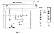
次に、上記TFT10および配線部20を備えた表示装置の一例を、図2を用いて説明する。図2は極薄型の有機発光カラーディスプレイとして用いられる表示装置1の構成を表したものである。この表示装置1は、例えば、TFT10を備えた基板11に、表示素子として複数の有機発光素子よりなる画素PXLCがマトリクス状に配置されてなる表示領域110を有する。この表示領域30の周辺には、信号部である水平セレクタ(HSEL)31と、スキャナ部であるライトスキャナ(WSCN)32および電源スキャナ(DSCN)33とが形成されている。
(1-3) Overall Configuration of Display Element Next, an example of a display device including the
表示領域30において、列方向には信号線DTL1〜DTLnが配置され、行方向には走査線WSL1〜WSLmおよび電源ラインDSL1〜DSLmが配置されている。各信号線DTLと各走査線WSLとの交差点に、有機発光素子PXLC(赤色、青色および緑色のいずれか一つ(サブピクセル))を含む画素回路40が設けられている。各信号線DTLは、水平セレクタ31に接続され、この水平セレクタ31から信号線DTLに映像信号が供給される。各走査線WSLは、ライトスキャナ32に接続されている。各電源ラインDSLは、電源スキャナ33に接続されている。
In the
図3は、画素回路40の一例を表したものである。画素回路40は、サンプリング用トランジスタ3Aおよび駆動用トランジスタ3Bと、保持容量3Cと、有機発光素子PXLCよりなる発光素子3Dとを有するアクティブ型の駆動回路である。これらトランジスタ3A,3Bは上記本発明の薄膜トランジスタにより構成されている。
FIG. 3 illustrates an example of the
サンプリング用トランジスタ3Aは、そのゲートが対応する走査線WSL1に接続され、そのソースおよびドレインの一方が対応する信号線DTL1に接続され、他方が駆動用トランジスタ3Bのゲートgに接続されている。駆動用トランジスタ3Bは、そのドレインdが対応する電源線DSL1に接続され、ソースsが発光素子3Dのアノードに接続されている。発光素子3Dのカソードは接地配線3Hに接続されている。なお、この接地配線3Hは全ての画素PXLCに対して共通に配線されている。保持容量3Cは駆動用トランジスタ3Bのソースsとゲートgとの間に接続されている。
サンプリング用トランジスタ3Aは、走査線WSL1から供給される制御信号に応じて導通し、信号線DTL1から供給された映像信号の信号電位をサンプリングして保持容量3Cに保持するものである。駆動用トランジスタ3Bは、第1電位にある電源線DSL1から電流の供給を受け、保持容量3Cに保持された信号電位に応じて駆動電流を発光素子3Dに供給するものである。発光素子3Dは、供給された駆動電流により、映像信号の信号電位に応じた輝度で発光するようになっている。
The
この表示装置1では、走査線WSLから供給される制御信号に応じてサンプリング用トランジスタ3Aが導通し、信号線DTLから供給された映像信号の信号電位がサンプリングされて保持容量3Cに保持される。また、第1電位にある電源線DSLから駆動用トランジスタ3Bに電流が供給され、保持容量3Cに保持された信号電位に応じて、駆動電流が発光素子3D(赤色、青色および緑色の各有機発光素子)に供給される。各発光素子3Dは供給された駆動電流により映像信号の信号電位に応じた輝度で発光する。
In the
この表示装置1は、例えば次のようにして製造することができる。
The
(製造方法)
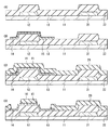
まず、図4(A)に示したように、ガラスよりなる基板11上に、例えばスパッタ法により、例えばモリブデン(Mo)層を成膜した後、フォトリソグラフィおよびドライエッチングによりゲート電極12および第1配線層21を形成する。続いて、例えば、基板11の全面に例えばプラズマCVD(Chemical Vapor Deposition ;化学気相成長)法により厚さ200nmのSiOxを成膜しゲート絶縁膜13および第1絶縁層22を形成する。
(Production method)
First, as shown in FIG. 4A, after a molybdenum (Mo) layer, for example, is formed on a
次に、図4(B)に示したように、真空中において例えば、In−Ga−Znの酸化物ターゲットを用いたスパッタ法により半導体層14Aを成膜する。続いて、第1保護膜15としてCVD法により厚さ20nmのSiOxを成膜したのち、フォトリソグラフィおよび例えば希フッ酸系溶液を用いたエッチングにより第1保護膜15と共に半導体層14Aを加工し、ゲート電極13に対向する領域にチャネル層14を形成する。
Next, as illustrated in FIG. 4B, the
続いて、図4(C)に示したように、第1絶縁膜15およびゲート絶縁膜13の全面に例えばプラズマCVD法により厚さ200nmのSiOxを成膜し第2保護膜16および第2絶縁膜23を形成する。
Subsequently, as shown in FIG. 4C, SiO x having a thickness of 200 nm is formed on the entire surfaces of the first insulating
次に、図4(D)に示したように、例えばフォトリソグラフィによるレジストのパターニングとドライエッチングによりチャネル層14と次の工程において形成するソース・ドレイン電極17とのコンタクト領域を形成する。具体的には、CF4系ガスを用いることにより第1保護膜15および第2保護膜16を同時に所定の形状に加工する。
Next, as shown in FIG. 4D, contact regions between the
続いて、例えばスパッタ法を用いてTi/Al/Moをそれぞれ50nm,900nm,50nmの膜厚で成膜し、例えば酸素添加のCl2CF4ガスによるドライエッチングによりソース・ドレイン電極17および第2配線層24を形成する。これにより、配線部20が形成される。最後に、チャネル層14中の酸素欠損をなくすために熱処理を行う。具体的には、例えば窒素および酸素の雰囲気下、酸素濃度約40%、温度300度、2時間の熱処理を行うことでTFT10形成される。以上により本実施の形態の表示装置1が完成する。
Subsequently, Ti / Al / Mo is deposited to a thickness of 50 nm, 900 nm, and 50 nm, for example, by sputtering, and the source / drain electrode 17 and the second electrode 17 are formed by dry etching using, for example, oxygen-added Cl 2 CF 4 gas. A wiring layer 24 is formed. Thereby, the
図5は従来の表示装置100の断面構成を表したものである。この表示装置100を構成するTFT110にはチャネル層114上には1層の保護膜116が設けられており、配線部120には第1絶縁膜122と第2絶縁膜122との間に半導体層114Aが挟持されている。
FIG. 5 illustrates a cross-sectional configuration of a conventional display device 100. The TFT 110 constituting the display device 100 is provided with a single protective film 116 on the
図6は従来の表示装置100の製造工程を表したものである。以下に各工程を簡単に説明する。まず、図6(A)に示したように、基板111上にゲート電極および第1配線層を形成したのち、基板111、ゲート電極112および第1配線層121の全面にゲート絶縁膜113および第1絶縁膜122を形成する。続いて、図6(B)に示したように、ゲート絶縁膜113上に半導体層114および保護膜116(第2保護膜16およびだい2絶縁膜23に相当)を形成する。次に、図6(C)に示したように保護膜116をフォトリソグラフィおよびエッチングにより加工したのち、図6(D)に示したように半導体層114Aをフォトリソグラフィおよびエッチングにより加工してチャネル層114を形成する。最後に、保護膜116、チャネル層114および基板111の全面にソース・ドレイン電極117および第2配線層124に対応するメタル層を成膜および加工することにより表示装置100が完成する。
FIG. 6 shows a manufacturing process of the conventional display device 100. Each process will be briefly described below. First, as shown in FIG. 6A, after a gate electrode and a first wiring layer are formed over the
以上のように製造された表示装置100では、TFT110および配線部120において以下の問題が生じる。まず、TFT110では、全面に成膜した保護膜116を所定の形状に加工するためにエッチングを行うが、その際、保護膜116の下層のチャネル層114が露出しているためエッチングのための各種プラズマあるいはエッチング液等に曝される。これによりチャネル層114の表面が損傷し、TFT110の特性が劣化する。また、配線部120では、第1絶縁膜122と第2絶縁膜123との間に半導体層114Aが残存するため、第2絶縁膜123の表面から基板111にかけて形成される第2配線層124と短絡が生じる。これにより、第1配線層121と第2配線層124との間のクロス容量は実質第1絶縁膜の膜厚となる。即ち、クロス容量の増大により、信号の伝達等に不具合が生じる等の信頼性が低下するという問題があった。
In the display device 100 manufactured as described above, the following problems occur in the TFT 110 and the
本実施の形態は、チャネル層14(半導体層14A)上に第1保護膜15を形成するようにしたものである。これにより、TFT10では各種プラズマ等によるチャネル層14の損傷を防ぐことが可能となる。また、本実施の形態は、ゲート電極13に対向する領域以外の半導体層14Aを第1保護膜15と共に除去、即ち、第1配線層の上部の領域のチャネル層を除去するようにしたものである。これにより、配線部20では第1絶縁膜22および第2絶縁膜23が直接積層される。即ち、第1配線層21と第2配線層24との間の十分な膜厚を確保することが可能となる。
In the present embodiment, the first
図7は比較例(図7(A))および本実施の形態の実施例(図7(B))の面内における電流電圧特性を表したものである。図7(A)では、ばらつきがあるのに対し、図7(B)ではばらつきは見られない。このことから本実施の形態の製造方法によってTFTを製造することによってTFT特性のばらつきが低減されたことがわかる。 FIG. 7 shows in-plane current-voltage characteristics of the comparative example (FIG. 7A) and the example of the present embodiment (FIG. 7B). In FIG. 7A, there is variation, whereas in FIG. 7B, there is no variation. From this, it can be seen that the variation in TFT characteristics is reduced by manufacturing the TFT by the manufacturing method of the present embodiment.
このように本実施の形態の表示装置およびその製造方法では、チャネル層14上に第1保護膜15を形成するようにしたので、第2保護膜の加工時におけるチャネル層14表面の損傷が防止され、TFT10の特性劣化を抑制することが可能となる。また、第1配線層21上の半導体層14Aを除去することにより、第1配線層21と第2配線層24との間の膜厚が確保される。即ち、第1配線層21と第2配線層24とのクロス容量が低減される。従って表示装置の信頼性が向上する。
As described above, in the display device and the manufacturing method thereof according to the present embodiment, since the first
(モジュールおよび適用例)
続いて表示装置の適用例について説明する。上記表示装置は、テレビジョン装置,デジタルカメラ,ノート型パーソナルコンピュータ、携帯電話等の携帯端末装置あるいはビデオカメラなど、外部から入力された映像信号あるいは内部で生成した映像信号を、画像あるいは映像として表示するあらゆる分野の電子機器の表示装置として用いることが可能である。
(Modules and application examples)
Next, application examples of the display device will be described. The display device displays an externally input video signal or an internally generated video signal as an image or video, such as a television device, a digital camera, a notebook personal computer, a mobile terminal device such as a mobile phone, or a video camera. It can be used as a display device for electronic devices in all fields.
(モジュール)
例えば図8に示したようなモジュールとして、後述する適用例1〜5などの種々の電子機器に組み込まれる。このモジュールは、例えば、基板11の一辺に、封止用基板50および接着層(図示せず)から露出した領域210を設け、この露出した領域210に、水平セレクタ31,ライトスキャナ32および電源スキャナ33の配線を延長して外部接続端子(図示せず)を形成したものである。外部接続端子には、信号の入出力のためのフレキシブルプリント配線基板(FPC;Flexible Printed Circuit)220が設けられていてもよい。
(module)
For example, the module shown in FIG. 8 is incorporated into various electronic devices such as application examples 1 to 5 described later. In this module, for example, a
(適用例1)
図9は上記表示装置が適用されるテレビジョン装置の外観を表したものである。このテレビジョン装置は、例えば、フロントパネル310およびフィルターガラス320を含む映像表示画面部300を有しており、この映像表示画面部300は、上記各実施の形態に係る表示装置により構成されている。
(Application example 1)
FIG. 9 shows an appearance of a television device to which the display device is applied. The television apparatus has, for example, a video display screen unit 300 including a front panel 310 and a filter glass 320, and the video display screen unit 300 is configured by the display device according to each of the above embodiments. .
(適用例2)
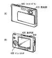
図10は上記表示装置が適用されるデジタルカメラの外観を表したものである。このデジタルカメラは、例えば、フラッシュ用の発光部410、表示部420、メニュースイッチ430およびシャッターボタン440を有しており、その表示部420は、上記各実施の形態に係る表示装置により構成されている。
(Application example 2)
FIG. 10 shows the appearance of a digital camera to which the display device is applied. The digital camera includes, for example, a flash light emitting unit 410, a display unit 420, a menu switch 430, and a
(適用例3)
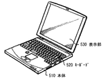
図11は上記表示装置が適用されるノート型パーソナルコンピュータの外観を表したものである。このノート型パーソナルコンピュータは、例えば、本体510,文字等の入力操作のためのキーボード520および画像を表示する表示部530を有しており、その表示部530は、上記各実施の形態に係る表示装置により構成されている。
(Application example 3)
FIG. 11 shows the appearance of a notebook personal computer to which the display device is applied. The notebook personal computer has, for example, a main body 510, a keyboard 520 for inputting characters and the like, and a display unit 530 for displaying an image. The display unit 530 is a display according to each of the above embodiments. It is comprised by the apparatus.
(適用例4)
図12は上記表示装置が適用されるビデオカメラの外観を表したものである。このビデオカメラは、例えば、本体部610,この本体部610の前方側面に設けられた被写体撮影用のレンズ620,撮影時のスタート/ストップスイッチ630および表示部640を有しており、その表示部640は上記表示装置により構成されている。
(Application example 4)
FIG. 12 shows the appearance of a video camera to which the display device is applied. This video camera has, for example, a main body 610, a
(適用例5)
図13は上記表示装置が適用される携帯電話機の外観を表したものである。この携帯電話機は、例えば上側筐体710と下側筐体720とを連結部(ヒンジ部)730で連結したものであり、ディスプレイ740,サブディスプレイ750,ピクチャーライト760およびカメラ770を有している。そのディスプレイ740またはサブディスプレイ750は、上記表示装置により構成されている。
(Application example 5)
FIG. 13 shows an appearance of a mobile phone to which the display device is applied. This mobile phone is obtained by connecting, for example, an
以上、実施の形態を挙げて本発明の表示装置1について説明したが、本発明は上記実施の形態に限定されるものではなく、本発明の表示装置1の構成およびその製造方法は、上記実施の形態と同様の効果を得ることが可能な限りにおいて自由に変形可能である。
The
例えば、上記実施の形態では、チャネル層14の材料として、In−Ga−Znを用いたが、Gaの代わりにAlあるいはFeを用いてもよい。また、上記実施の形態ではソース・ドレイン電極17はTi/Al/Moからなる3層としたが、例えばMo/Al/MoあるいはTi/Al/Tiからなる3層としてもよい。また、上記実施の形態では、スパッタ法によりチャネル層14を真空中で成膜したのち、一旦大気中に出してCVD法にて第1保護膜15、第2保護膜16をこの順に成膜したが、スパッタ装置とCVD装置をクラスター化した装置により、各層14,15,16を真空中にて連続成膜してもよい。
For example, although In—Ga—Zn is used as the material of the
1…表示装置、10…TFT(薄膜トランジスタ)、11…基板、12…ゲート電極、13…ゲート絶縁膜、14…チャネル層、14A…半導体層、15…第1保護膜、16…第2保護膜、17…ソース・ドレイン電極、20…配線部、21…第1配線層、22…第1絶縁膜、23…第2絶縁膜、24…第2配線層。
DESCRIPTION OF
Claims (6)
前記薄膜トランジスタは、
ゲート電極と、
酸化物半導体を主成分とするチャネル層と、
前記ゲート電極とチャネル層との間に設けられたゲート絶縁膜と、
前記チャネル層に接すると共に、前記ゲート電極とは反対側に設けられた第1保護膜と、
前記第1保護膜上に設けられた第2保護膜と、
前記チャネル層に接触し、ソース・ドレイン電極となる一対の電極とを有し、
前記配線部は、
第1配線と、
前記第1配線に対向する第2配線と、
前記第1配線と第2配線との間に設けられると共に、前記ゲート絶縁膜に連なる第1絶縁膜と前記第2保護膜に連なる第2絶縁膜との積層構造を有する絶縁層とを有する
表示装置。 A thin film transistor and a wiring portion;
The thin film transistor
A gate electrode;
A channel layer mainly composed of an oxide semiconductor;
A gate insulating film provided between the gate electrode and the channel layer;
A first protective film in contact with the channel layer and provided on the opposite side of the gate electrode;
A second protective film provided on the first protective film;
A pair of electrodes that contact the channel layer and serve as source / drain electrodes;
The wiring part is
A first wiring;
A second wiring facing the first wiring;
An insulating layer provided between the first wiring and the second wiring and having a stacked structure of a first insulating film connected to the gate insulating film and a second insulating film connected to the second protective film. apparatus.
前記ゲート電極上および前記第1配線層上にそれぞれゲート絶縁膜および第1絶縁膜を形成したのち、前記ゲート絶縁膜および第1絶縁膜上に酸化物半導体を主成分とする半導体層を形成する工程と、
前記半導体層上に第1保護膜を形成したのち、前記半導体層および第1保護膜をエッチングし加工しゲート電極に対向する領域に、前記第1保護膜を積層する酸化物半導体を主成分とするチャネル層を形成すると共に、少なくとも前記第1配線層に対向する領域の前記半導体層および第1保護膜を除去する工程と、
前記第1保護膜および前記第1絶縁膜上にそれぞれ第2保護膜および第2絶縁膜を形成したのち、前記第2保護膜をエッチングし加工する工程と、
前記チャネル層に接するようにソース・ドレインとなる一対の電極を形成すると共に、少なくとも前記第1配線層に対向する位置に第2配線層を形成する工程と
を含む表示装置の製造方法。 Forming a gate electrode and a first wiring layer on the substrate;
After forming a gate insulating film and a first insulating film on the gate electrode and the first wiring layer, respectively, a semiconductor layer containing an oxide semiconductor as a main component is formed on the gate insulating film and the first insulating film. Process,
After forming the first protective film on the semiconductor layer, the semiconductor layer and the first protective film are etched and processed, and an oxide semiconductor in which the first protective film is stacked in a region facing the gate electrode is a main component. Forming a channel layer to be removed and at least removing the semiconductor layer and the first protective film in a region facing the first wiring layer;
Forming a second protective film and a second insulating film on the first protective film and the first insulating film, respectively, and then etching and processing the second protective film;
Forming a pair of electrodes serving as a source and a drain so as to be in contact with the channel layer, and forming a second wiring layer at a position facing at least the first wiring layer.
Priority Applications (2)
| Application Number | Priority Date | Filing Date | Title |
|---|---|---|---|
| JP2011066747A JP2012204548A (en) | 2011-03-24 | 2011-03-24 | Display device and manufacturing method therefor |
| US13/403,735 US8673661B2 (en) | 2011-03-24 | 2012-02-23 | Display apparatus and method of manufacturing the same |
Applications Claiming Priority (1)
| Application Number | Priority Date | Filing Date | Title |
|---|---|---|---|
| JP2011066747A JP2012204548A (en) | 2011-03-24 | 2011-03-24 | Display device and manufacturing method therefor |
Publications (2)
| Publication Number | Publication Date |
|---|---|
| JP2012204548A true JP2012204548A (en) | 2012-10-22 |
| JP2012204548A5 JP2012204548A5 (en) | 2014-05-01 |
Family
ID=46876574
Family Applications (1)
| Application Number | Title | Priority Date | Filing Date |
|---|---|---|---|
| JP2011066747A Pending JP2012204548A (en) | 2011-03-24 | 2011-03-24 | Display device and manufacturing method therefor |
Country Status (2)
| Country | Link |
|---|---|
| US (1) | US8673661B2 (en) |
| JP (1) | JP2012204548A (en) |
Cited By (2)
| Publication number | Priority date | Publication date | Assignee | Title |
|---|---|---|---|---|
| WO2014080826A1 (en) * | 2012-11-21 | 2014-05-30 | シャープ株式会社 | Display apparatus |
| JP2014207292A (en) * | 2013-04-11 | 2014-10-30 | 株式会社ジャパンディスプレイ | Thin film transistor and display device using the same |
Families Citing this family (3)
| Publication number | Priority date | Publication date | Assignee | Title |
|---|---|---|---|---|
| JP2012204548A (en) * | 2011-03-24 | 2012-10-22 | Sony Corp | Display device and manufacturing method therefor |
| US20160104669A1 (en) * | 2014-10-08 | 2016-04-14 | Infineon Technologies Ag | Semiconductor structure with improved metallization adhesion and method for manufacturing the same |
| CN107293493A (en) * | 2017-06-06 | 2017-10-24 | 武汉华星光电技术有限公司 | The preparation method of indium gallium zinc oxide thin film transistor (TFT) |
Citations (9)
| Publication number | Priority date | Publication date | Assignee | Title |
|---|---|---|---|---|
| JP2006186119A (en) * | 2004-12-28 | 2006-07-13 | Casio Comput Co Ltd | Thin film transistor and manufacturing method thereof |
| JP2007073559A (en) * | 2005-09-02 | 2007-03-22 | Kochi Prefecture Sangyo Shinko Center | Thin film transistor manufacturing method |
| JP2007096055A (en) * | 2005-09-29 | 2007-04-12 | Semiconductor Energy Lab Co Ltd | Semiconductor device and manufacturing method of semiconductor device |
| JP2007134687A (en) * | 2005-10-14 | 2007-05-31 | Semiconductor Energy Lab Co Ltd | Semiconductor device and manufacturing method thereof |
| JP2009260378A (en) * | 2005-09-29 | 2009-11-05 | Semiconductor Energy Lab Co Ltd | Method of manufacturing semiconductor device |
| JP2010123913A (en) * | 2008-11-21 | 2010-06-03 | Korea Electronics Telecommun | Thin-film transistor and method of manufacturing the same |
| JP2010182818A (en) * | 2009-02-04 | 2010-08-19 | Sony Corp | Thin-film transistor, and display device |
| JP2011009719A (en) * | 2009-05-29 | 2011-01-13 | Semiconductor Energy Lab Co Ltd | Semiconductor device and method of manufacturing the same |
| JP2011049548A (en) * | 2009-07-31 | 2011-03-10 | Semiconductor Energy Lab Co Ltd | Semiconductor device and method for manufacturing the same |
Family Cites Families (32)
| Publication number | Priority date | Publication date | Assignee | Title |
|---|---|---|---|---|
| JPS6319876A (en) * | 1986-07-11 | 1988-01-27 | Fuji Xerox Co Ltd | Thin film transistor device |
| JP2771820B2 (en) * | 1988-07-08 | 1998-07-02 | 株式会社日立製作所 | Active matrix panel and manufacturing method thereof |
| KR970004885B1 (en) * | 1993-05-12 | 1997-04-08 | 삼성전자 주식회사 | Flat display device and its making method |
| JP3344072B2 (en) * | 1994-03-31 | 2002-11-11 | ソニー株式会社 | Method for manufacturing thin film transistor |
| JPH08184853A (en) * | 1994-12-27 | 1996-07-16 | Sharp Corp | Active matrix substrate manufacturing method and active matrix substrate |
| KR100190041B1 (en) * | 1995-12-28 | 1999-06-01 | 윤종용 | Manufacturing method of liquid crystal display device |
| JP3433632B2 (en) * | 1996-12-10 | 2003-08-04 | カシオ計算機株式会社 | Method for manufacturing thin film transistor |
| US5998230A (en) * | 1998-10-22 | 1999-12-07 | Frontec Incorporated | Method for making liquid crystal display device with reduced mask steps |
| JP2001119029A (en) * | 1999-10-18 | 2001-04-27 | Fujitsu Ltd | Thin film transistor, method of manufacturing the same, and liquid crystal display device having the same |
| JP2002237594A (en) * | 2001-02-02 | 2002-08-23 | Internatl Business Mach Corp <Ibm> | Thin film transistor, method of manufacturing thin film transistor, and display device including thin film transistor |
| WO2005050597A1 (en) * | 2003-11-14 | 2005-06-02 | Semiconductor Energy Laboratory Co., Ltd. | Light-emitting device and method for manufacturing the same |
| KR101353269B1 (en) * | 2006-12-11 | 2014-01-20 | 삼성디스플레이 주식회사 | Thin film transistor substrate and method for manufacturing the same |
| KR101410926B1 (en) | 2007-02-16 | 2014-06-24 | 삼성전자주식회사 | Thin film transistor and manufacturing method thereof |
| TWI387109B (en) * | 2008-06-10 | 2013-02-21 | Taiwan Tft Lcd Ass | Method for manufacturing thin film transistor |
| JP5584960B2 (en) * | 2008-07-03 | 2014-09-10 | ソニー株式会社 | Thin film transistor and display device |
| TWI622175B (en) * | 2008-07-31 | 2018-04-21 | 半導體能源研究所股份有限公司 | Semiconductor device |
| EP2172977A1 (en) * | 2008-10-03 | 2010-04-07 | Semiconductor Energy Laboratory Co., Ltd. | Display device |
| JP5515281B2 (en) * | 2008-12-03 | 2014-06-11 | ソニー株式会社 | THIN FILM TRANSISTOR, DISPLAY DEVICE, ELECTRONIC DEVICE, AND METHOD FOR PRODUCING THIN FILM TRANSISTOR |
| JP2010182819A (en) * | 2009-02-04 | 2010-08-19 | Sony Corp | Thin-film transistor, and display device |
| US8450144B2 (en) * | 2009-03-26 | 2013-05-28 | Semiconductor Energy Laboratory Co., Ltd. | Semiconductor device and method for manufacturing the same |
| TWI617029B (en) * | 2009-03-27 | 2018-03-01 | 半導體能源研究所股份有限公司 | Semiconductor device |
| TWI476917B (en) * | 2009-04-16 | 2015-03-11 | 半導體能源研究所股份有限公司 | Semiconductor device and method of manufacturing same |
| WO2011055474A1 (en) * | 2009-11-09 | 2011-05-12 | シャープ株式会社 | Active matrix substrate, liquid crystal display panel provided with same, and method for manufacturing active matrix substrate |
| EP2518772A4 (en) * | 2009-12-21 | 2016-09-07 | Sharp Kk | ACTIVE MATRIX SUBSTRATE, DISPLAY PANEL HAVING AN ACTIVE MATRIX SUBSTRATE, AND METHOD FOR MANUFACTURING THE SUBSTRATE |
| KR101711870B1 (en) * | 2009-12-23 | 2017-03-06 | 삼성디스플레이 주식회사 | Thin film transistor, manufacturing method thereof and display substrate using the thin film transistor |
| JP5668917B2 (en) * | 2010-11-05 | 2015-02-12 | ソニー株式会社 | Thin film transistor and manufacturing method thereof |
| JP2012204548A (en) * | 2011-03-24 | 2012-10-22 | Sony Corp | Display device and manufacturing method therefor |
| TWI455322B (en) * | 2011-04-22 | 2014-10-01 | Au Optronics Corp | Thin film transistor and method of manufacturing same |
| KR101854197B1 (en) * | 2011-05-12 | 2018-06-21 | 삼성디스플레이 주식회사 | Array substrate and method of manufacturing the same |
| KR101425064B1 (en) * | 2011-06-09 | 2014-08-01 | 엘지디스플레이 주식회사 | Oxide thin film transistor and method of fabricating the same |
| KR20130021607A (en) * | 2011-08-23 | 2013-03-06 | 삼성디스플레이 주식회사 | Low resistance conductive line, thin film transistor, thin film transistor panel and method of manufacturing the same |
| CN102800709B (en) * | 2012-09-11 | 2015-07-01 | 深圳市华星光电技术有限公司 | Driving device for thin film transistor |
-
2011
- 2011-03-24 JP JP2011066747A patent/JP2012204548A/en active Pending
-
2012
- 2012-02-23 US US13/403,735 patent/US8673661B2/en active Active
Patent Citations (9)
| Publication number | Priority date | Publication date | Assignee | Title |
|---|---|---|---|---|
| JP2006186119A (en) * | 2004-12-28 | 2006-07-13 | Casio Comput Co Ltd | Thin film transistor and manufacturing method thereof |
| JP2007073559A (en) * | 2005-09-02 | 2007-03-22 | Kochi Prefecture Sangyo Shinko Center | Thin film transistor manufacturing method |
| JP2007096055A (en) * | 2005-09-29 | 2007-04-12 | Semiconductor Energy Lab Co Ltd | Semiconductor device and manufacturing method of semiconductor device |
| JP2009260378A (en) * | 2005-09-29 | 2009-11-05 | Semiconductor Energy Lab Co Ltd | Method of manufacturing semiconductor device |
| JP2007134687A (en) * | 2005-10-14 | 2007-05-31 | Semiconductor Energy Lab Co Ltd | Semiconductor device and manufacturing method thereof |
| JP2010123913A (en) * | 2008-11-21 | 2010-06-03 | Korea Electronics Telecommun | Thin-film transistor and method of manufacturing the same |
| JP2010182818A (en) * | 2009-02-04 | 2010-08-19 | Sony Corp | Thin-film transistor, and display device |
| JP2011009719A (en) * | 2009-05-29 | 2011-01-13 | Semiconductor Energy Lab Co Ltd | Semiconductor device and method of manufacturing the same |
| JP2011049548A (en) * | 2009-07-31 | 2011-03-10 | Semiconductor Energy Lab Co Ltd | Semiconductor device and method for manufacturing the same |
Cited By (4)
| Publication number | Priority date | Publication date | Assignee | Title |
|---|---|---|---|---|
| WO2014080826A1 (en) * | 2012-11-21 | 2014-05-30 | シャープ株式会社 | Display apparatus |
| JPWO2014080826A1 (en) * | 2012-11-21 | 2017-01-05 | シャープ株式会社 | Display device |
| JP2014207292A (en) * | 2013-04-11 | 2014-10-30 | 株式会社ジャパンディスプレイ | Thin film transistor and display device using the same |
| US10283644B2 (en) | 2013-04-11 | 2019-05-07 | Japan Display Inc. | Thin film transistor having stable threshold voltage and less parasitic capacitance, and display device using the same |
Also Published As
| Publication number | Publication date |
|---|---|
| US8673661B2 (en) | 2014-03-18 |
| US20120241744A1 (en) | 2012-09-27 |
Similar Documents
| Publication | Publication Date | Title |
|---|---|---|
| US8748878B2 (en) | Thin film transistor, method of manufacturing the same, and display device | |
| US11532686B2 (en) | Array substrate, display apparatus, and method of fabricating array substrate | |
| CN106898551B (en) | Method of manufacturing thin film transistor, thin film transistor substrate and flat panel display device | |
| CN101800248B (en) | Thin film transistor and display unit | |
| JP5668917B2 (en) | Thin film transistor and manufacturing method thereof | |
| US11695016B2 (en) | Active matrix substrate and method for manufacturing same | |
| JP5743064B2 (en) | THIN FILM TRANSISTOR, MANUFACTURING METHOD THEREOF, AND DISPLAY DEVICE | |
| US9721977B2 (en) | Display device and electronic unit | |
| TWI497725B (en) | Display and electronic unit | |
| US20110215328A1 (en) | Thin film transistor, method of manufacturing the thin film transistor, and display device | |
| US9312279B2 (en) | Thin film transistor array substrate, method of manufacturing the same, and display apparatus including the same | |
| US10825876B2 (en) | Display device and method of manufacturing the same | |
| CN104078511B (en) | Semiconductor devices, display unit and electronic installation | |
| US9711576B2 (en) | Display, method of manufacturing display and electronic device | |
| JP2010182818A (en) | Thin-film transistor, and display device | |
| CN103247692A (en) | Thin-film transistor, display unit, and electronic apparatus | |
| JP2014229814A (en) | Thin-film transistor, display device, and electronic apparatus | |
| JP6175740B2 (en) | THIN FILM TRANSISTOR, MANUFACTURING METHOD THEREOF, DISPLAY DEVICE AND ELECTRONIC DEVICE | |
| CN102683383A (en) | Display device and electronic device | |
| US8673661B2 (en) | Display apparatus and method of manufacturing the same | |
| JP6019330B2 (en) | THIN FILM TRANSISTOR, METHOD FOR PRODUCING THIN FILM TRANSISTOR, DISPLAY DEVICE, AND ELECTRONIC DEVICE |
Legal Events
| Date | Code | Title | Description |
|---|---|---|---|
| A521 | Request for written amendment filed |
Free format text: JAPANESE INTERMEDIATE CODE: A523 Effective date: 20140317 |
|
| A621 | Written request for application examination |
Free format text: JAPANESE INTERMEDIATE CODE: A621 Effective date: 20140317 |
|
| A131 | Notification of reasons for refusal |
Free format text: JAPANESE INTERMEDIATE CODE: A131 Effective date: 20141224 |
|
| A977 | Report on retrieval |
Free format text: JAPANESE INTERMEDIATE CODE: A971007 Effective date: 20141225 |
|
| A521 | Request for written amendment filed |
Free format text: JAPANESE INTERMEDIATE CODE: A523 Effective date: 20150120 |
|
| A02 | Decision of refusal |
Free format text: JAPANESE INTERMEDIATE CODE: A02 Effective date: 20150324 |