JP2012204643A - Semiconductor device - Google Patents
Semiconductor device Download PDFInfo
- Publication number
- JP2012204643A JP2012204643A JP2011068358A JP2011068358A JP2012204643A JP 2012204643 A JP2012204643 A JP 2012204643A JP 2011068358 A JP2011068358 A JP 2011068358A JP 2011068358 A JP2011068358 A JP 2011068358A JP 2012204643 A JP2012204643 A JP 2012204643A
- Authority
- JP
- Japan
- Prior art keywords
- circuit
- buffer
- region
- semiconductor device
- area
- Prior art date
- Legal status (The legal status is an assumption and is not a legal conclusion. Google has not performed a legal analysis and makes no representation as to the accuracy of the status listed.)
- Ceased
Links
- 239000004065 semiconductor Substances 0.000 title claims abstract description 30
- 239000000872 buffer Substances 0.000 claims abstract description 172
- 238000006243 chemical reaction Methods 0.000 claims description 13
- 230000002093 peripheral effect Effects 0.000 abstract description 15
- 238000010586 diagram Methods 0.000 description 30
- 230000000694 effects Effects 0.000 description 13
- 230000012447 hatching Effects 0.000 description 4
- 235000014676 Phragmites communis Nutrition 0.000 description 3
- 230000000052 comparative effect Effects 0.000 description 3
- 230000005540 biological transmission Effects 0.000 description 2
- 230000003139 buffering effect Effects 0.000 description 2
- 230000004044 response Effects 0.000 description 2
- 230000003213 activating effect Effects 0.000 description 1
- 230000015572 biosynthetic process Effects 0.000 description 1
- 238000009792 diffusion process Methods 0.000 description 1
- 230000001788 irregular Effects 0.000 description 1
- 238000012986 modification Methods 0.000 description 1
- 230000004048 modification Effects 0.000 description 1
- 230000001151 other effect Effects 0.000 description 1
Images






Classifications
-
- G—PHYSICS
- G11—INFORMATION STORAGE
- G11C—STATIC STORES
- G11C11/00—Digital stores characterised by the use of particular electric or magnetic storage elements; Storage elements therefor
- G11C11/21—Digital stores characterised by the use of particular electric or magnetic storage elements; Storage elements therefor using electric elements
- G11C11/34—Digital stores characterised by the use of particular electric or magnetic storage elements; Storage elements therefor using electric elements using semiconductor devices
- G11C11/40—Digital stores characterised by the use of particular electric or magnetic storage elements; Storage elements therefor using electric elements using semiconductor devices using transistors
- G11C11/401—Digital stores characterised by the use of particular electric or magnetic storage elements; Storage elements therefor using electric elements using semiconductor devices using transistors forming cells needing refreshing or charge regeneration, i.e. dynamic cells
- G11C11/4063—Auxiliary circuits, e.g. for addressing, decoding, driving, writing, sensing or timing
- G11C11/407—Auxiliary circuits, e.g. for addressing, decoding, driving, writing, sensing or timing for memory cells of the field-effect type
- G11C11/409—Read-write [R-W] circuits
- G11C11/4093—Input/output [I/O] data interface arrangements, e.g. data buffers
-
- G—PHYSICS
- G11—INFORMATION STORAGE
- G11C—STATIC STORES
- G11C11/00—Digital stores characterised by the use of particular electric or magnetic storage elements; Storage elements therefor
- G11C11/21—Digital stores characterised by the use of particular electric or magnetic storage elements; Storage elements therefor using electric elements
- G11C11/34—Digital stores characterised by the use of particular electric or magnetic storage elements; Storage elements therefor using electric elements using semiconductor devices
- G11C11/40—Digital stores characterised by the use of particular electric or magnetic storage elements; Storage elements therefor using electric elements using semiconductor devices using transistors
- G11C11/401—Digital stores characterised by the use of particular electric or magnetic storage elements; Storage elements therefor using electric elements using semiconductor devices using transistors forming cells needing refreshing or charge regeneration, i.e. dynamic cells
- G11C11/4063—Auxiliary circuits, e.g. for addressing, decoding, driving, writing, sensing or timing
- G11C11/407—Auxiliary circuits, e.g. for addressing, decoding, driving, writing, sensing or timing for memory cells of the field-effect type
- G11C11/409—Read-write [R-W] circuits
- G11C11/4097—Bit-line organisation, e.g. bit-line layout, folded bit lines
-
- G—PHYSICS
- G11—INFORMATION STORAGE
- G11C—STATIC STORES
- G11C29/00—Checking stores for correct operation ; Subsequent repair; Testing stores during standby or offline operation
- G11C29/02—Detection or location of defective auxiliary circuits, e.g. defective refresh counters
- G11C29/022—Detection or location of defective auxiliary circuits, e.g. defective refresh counters in I/O circuitry
-
- G—PHYSICS
- G11—INFORMATION STORAGE
- G11C—STATIC STORES
- G11C29/00—Checking stores for correct operation ; Subsequent repair; Testing stores during standby or offline operation
- G11C29/02—Detection or location of defective auxiliary circuits, e.g. defective refresh counters
- G11C29/028—Detection or location of defective auxiliary circuits, e.g. defective refresh counters with adaption or trimming of parameters
-
- H—ELECTRICITY
- H10—SEMICONDUCTOR DEVICES; ELECTRIC SOLID-STATE DEVICES NOT OTHERWISE PROVIDED FOR
- H10B—ELECTRONIC MEMORY DEVICES
- H10B12/00—Dynamic random access memory [DRAM] devices
- H10B12/30—DRAM devices comprising one-transistor - one-capacitor [1T-1C] memory cells
- H10B12/48—Data lines or contacts therefor
-
- H—ELECTRICITY
- H10—SEMICONDUCTOR DEVICES; ELECTRIC SOLID-STATE DEVICES NOT OTHERWISE PROVIDED FOR
- H10B—ELECTRONIC MEMORY DEVICES
- H10B12/00—Dynamic random access memory [DRAM] devices
- H10B12/50—Peripheral circuit region structures
-
- G—PHYSICS
- G11—INFORMATION STORAGE
- G11C—STATIC STORES
- G11C11/00—Digital stores characterised by the use of particular electric or magnetic storage elements; Storage elements therefor
- G11C11/21—Digital stores characterised by the use of particular electric or magnetic storage elements; Storage elements therefor using electric elements
- G11C11/34—Digital stores characterised by the use of particular electric or magnetic storage elements; Storage elements therefor using electric elements using semiconductor devices
- G11C11/40—Digital stores characterised by the use of particular electric or magnetic storage elements; Storage elements therefor using electric elements using semiconductor devices using transistors
- G11C11/401—Digital stores characterised by the use of particular electric or magnetic storage elements; Storage elements therefor using electric elements using semiconductor devices using transistors forming cells needing refreshing or charge regeneration, i.e. dynamic cells
Landscapes
- Engineering & Computer Science (AREA)
- Microelectronics & Electronic Packaging (AREA)
- Computer Hardware Design (AREA)
- Semiconductor Integrated Circuits (AREA)
- Dram (AREA)
- Design And Manufacture Of Integrated Circuits (AREA)
- Semiconductor Memories (AREA)
Abstract
Description
本発明は半導体装置に関し、特に、メモリセル領域上に複数のデータバスが規則的に配列されてなる半導体装置に関する。 The present invention relates to a semiconductor device, and more particularly to a semiconductor device in which a plurality of data buses are regularly arranged on a memory cell region.
DRAM(Dynamic Random Access Memory)などの半導体メモリデバイスには、多数のメモリセルが規則的に配置されたメモリセル領域が存在する。また、メモリセル領域の近傍には、複数のバッファ回路からなるバッファ領域が配置される。メモリセルとバッファ回路との接続は、メモリセル領域の上部に配置された複数のデータバスを介して行われる。上述の通り、メモリセル領域においては多数のメモリセルが規則的に配置されることから、複数のデータバスについても規則的に配置される(特許文献1参照)。 A semiconductor memory device such as a DRAM (Dynamic Random Access Memory) has a memory cell region in which a large number of memory cells are regularly arranged. A buffer area composed of a plurality of buffer circuits is arranged in the vicinity of the memory cell area. The connection between the memory cell and the buffer circuit is made through a plurality of data buses arranged above the memory cell region. As described above, since a large number of memory cells are regularly arranged in the memory cell region, a plurality of data buses are also regularly arranged (see Patent Document 1).
バッファ回路はそれぞれ対応するデータバスに接続される回路であることから、バッファ回路についても規則的に配置することが一般的である。例えば、バッファ回路の配列ピッチをデータバスの配列ピッチと一致させれば、データバスの延長線上にバッファ回路が配置されるため、最も単純にレイアウトすることが可能となる。 Since each buffer circuit is a circuit connected to a corresponding data bus, the buffer circuits are generally arranged regularly. For example, if the arrangement pitch of the buffer circuits is made coincident with the arrangement pitch of the data bus, the buffer circuit is arranged on the extended line of the data bus, so that the layout can be made simplest.
しかしながら、バッファ回路の配列ピッチをデータバスの配列ピッチに一致させると、内部電圧生成回路などの他の回路ブロックのレイアウトが大きく制限される。つまり、メモリセル領域には、多数のメモリセルが規則的に配置されるアレイ領域とデコーダなどが配置される非アレイ領域が存在するため、バッファ回路の配列ピッチをデータバスの配列ピッチに一致させると、アレイ領域に隣接する部分は全てバッファ領域として使用されてしまうため、内部電圧生成回路などの回路ブロックは非アレイ領域に隣接して配置するしかなく、当該回路ブロックに割当可能な面積が不足してしまう。これを補うためには、内部電圧生成回路などの回路ブロックの幅を拡大するとともに、形成エリアの形状を変形させる必要があるが、この場合には、バッファ領域と当該回路ブロックとの幅の相違によって無駄な空きスペースが生じ、チップ面積の増大を招くという問題があった。 However, if the arrangement pitch of the buffer circuits is matched with the arrangement pitch of the data bus, the layout of other circuit blocks such as the internal voltage generation circuit is greatly limited. In other words, in the memory cell area, there are an array area in which a large number of memory cells are regularly arranged and a non-array area in which a decoder and the like are arranged, so that the arrangement pitch of the buffer circuits is matched with the arrangement pitch of the data bus. Since all the parts adjacent to the array area are used as buffer areas, the circuit blocks such as the internal voltage generation circuit must be arranged adjacent to the non-array area, and the area that can be allocated to the circuit block is insufficient. Resulting in. In order to compensate for this, it is necessary to increase the width of the circuit block such as the internal voltage generation circuit and to change the shape of the formation area. In this case, however, the difference in width between the buffer area and the circuit block is required. As a result, there is a problem that a wasteful empty space is generated and the chip area is increased.
本発明による半導体装置は、第1の方向に延在する複数のデータバスが第1のピッチで第2の方向に配列されたメモリセル領域と、前記メモリセル領域の前記第2の方向に延在する辺に沿って配置され、対応する前記複数のデータバスにそれぞれ接続された複数のバッファ回路が設けられたバッファ領域と、を備え、前記バッファ領域上においては、前記第1の方向に延在する前記複数のデータバスが第2のピッチで前記第2の方向に配列され、前記第2のピッチは前記第1のピッチよりも小さいことを特徴とする。 A semiconductor device according to the present invention includes a memory cell region in which a plurality of data buses extending in a first direction are arranged in a second direction at a first pitch, and extending in the second direction of the memory cell region. And a buffer area provided with a plurality of buffer circuits respectively connected to the corresponding plurality of data buses, and extending in the first direction on the buffer area. The plurality of existing data buses are arranged in the second direction at a second pitch, and the second pitch is smaller than the first pitch.
本発明によれば、データバスの配列ピッチをバッファ領域上において縮小していることから、内部電圧生成回路などの回路ブロックに割当可能な面積を十分に確保することが可能となる。これにより、当該回路ブロックの幅拡大や形状の変形が不要となることから、無駄な空きスペースが生じにくく、チップ面積を縮小することが可能となる。 According to the present invention, since the arrangement pitch of the data buses is reduced on the buffer area, it is possible to sufficiently secure an area that can be allocated to a circuit block such as an internal voltage generation circuit. This eliminates the need to increase the width of the circuit block or to change the shape of the circuit block, so that a wasteful empty space is hardly generated and the chip area can be reduced.
以下、添付図面を参照しながら、本発明の好ましい実施の形態について詳細に説明する。 Hereinafter, preferred embodiments of the present invention will be described in detail with reference to the accompanying drawings.
図1は、本発明の好ましい実施形態による半導体装置10の全体構成を示すブロック図である。
FIG. 1 is a block diagram showing the overall configuration of a
本実施形態による半導体装置10はDRAMであり、図1に示すようにメモリセルアレイ11を備えている。メモリセルアレイ11には、互いに交差する複数のワード線WLと複数のビット線BLが設けられており、その交点にメモリセルMCが配置されている。ワード線WLの選択はロウデコーダ12によって行われ、ビット線BLの選択はカラムデコーダ13によって行われる。ビット線BLは、センス回路14内の対応するセンスアンプSAにそれぞれ接続されており、カラムデコーダ13により選択されたビット線BLは、センスアンプSAを介してアンプ回路15に接続される。
The
ロウデコーダ12、カラムデコーダ13、センス回路14及びアンプ回路15の動作は、アクセス制御回路20によって制御される。アクセス制御回路20には、アドレス端子21及びコマンド端子22を介してそれぞれ外部からアドレス信号ADD及びコマンド信号CMDが供給される。アクセス制御回路20は、アドレス信号ADD及びコマンド信号CMDを受け、これらに基づいてロウデコーダ12、カラムデコーダ13、センス回路14及びアンプ回路15を制御する。
The operations of the
具体的には、コマンド信号CMDが半導体装置10のアクティブ動作を示している場合には、アドレス信号ADDはロウデコーダ12に供給される。これに応答して、ロウデコーダ12はアドレス信号ADDが示すワード線WLを選択し、これにより対応するメモリセルMCがそれぞれビット線BLに接続される。その後、アクセス制御回路20は、所定のタイミングでセンス回路14を活性化させる。
Specifically, when the command signal CMD indicates an active operation of the
一方、コマンド信号CMDが半導体装置10のリード動作又はライト動作を示している場合には、アドレス信号ADDはカラムデコーダ13に供給される。これに応答して、カラムデコーダ13はアドレス信号ADDが示すビット線BLをアンプ回路15に接続する。これにより、リード動作時においては、センスアンプSAを介してメモリセルアレイ11から読み出されたリードデータDQがアンプ回路15を介してデータ端子23から外部に出力される。また、ライト動作時においては、データ端子23を介して外部から供給されたリードデータDQがアンプ回路15及びセンスアンプSAを介してメモリセルMCに書き込まれる。
On the other hand, when the command signal CMD indicates a read operation or a write operation of the
これら各回路ブロックは、それぞれ所定の内部電圧を動作電源として使用する。これら内部電源は、図1に示す電源回路30によって生成される。電源回路30は、電源端子31,32を介してそれぞれ供給される外部電位VDD及び接地電位VSSを受け、これらに基づいて内部電圧VPP,VPERI,VARYなどを生成する。尚、本明細書においてVDD,VPP,VPERI,VARYとは、当該電位のレベルを示すほか、接地電位VSSに対する電位差(電圧)をも示す。例えば、「VDD」とは、外部電位VDDの電位レベルそのものを指すほか、接地電位VSSに対する電位差(電圧)をも示す。VPP,VPERI,VARYについても同様である。本実施形態では、
VPP>VDD>VPERI≒VARY
である。内部電位VPPは外部電位VDDを昇圧することによって生成され、内部電位VPERI,VARYは外部電位VDDを降圧することによって生成される。
Each of these circuit blocks uses a predetermined internal voltage as an operating power supply. These internal power supplies are generated by the
VPP>VDD> VPERI ≒ VARY
It is. The internal potential VPP is generated by boosting the external potential VDD, and the internal potentials VPERI and VARY are generated by stepping down the external potential VDD.
内部電圧VPPは、主にロウデコーダ12において用いられる電圧である。ロウデコーダ12は、アドレス信号ADDに基づき選択したワード線WLをVPPレベルに駆動し、これによりメモリセルMCに含まれるセルトランジスタを導通させる。内部電圧VARYは、センス回路14において用いられる電圧である。センス回路14が活性化すると、ビット線対の一方をVARYレベル、他方をVSSレベルに駆動することにより、読み出されたリードデータの増幅を行う。内部電圧VPERIは、アクセス制御回路20などの大部分の周辺回路の動作電圧として用いられる。これら周辺回路の動作電圧として外部電圧VDDよりも電圧の低い内部電圧VPERIを用いることにより、半導体装置10の低消費電力化が図られている。
The internal voltage VPP is a voltage mainly used in the
次に、本実施形態による半導体装置10のレイアウトについて説明する。
Next, the layout of the
図2は、半導体装置10の主要部のレイアウト図である。
FIG. 2 is a layout diagram of the main part of the
図2に示すように、メモリセルアレイ11はメモリセル領域40に配置される。メモリセル領域40はX方向にいくつか分断されており、分断された部分が非アレイ領域40aとして用いられる。非アレイ領域40aには、図1に示したロウデコーダ12の一部やカラムデコーダ13の一部が配置される。メモリセル領域40の上部には、Y方向に延在する複数のデータバスDBがX方向に配列されている。
As shown in FIG. 2, the
図2に示すパッド領域50は、複数の外部端子がX方向に配列された領域である。したがって、図1に示したアドレス端子21、コマンド端子22、データ端子23及び電源端子31,32は、このパッド領域50に配置される。
The
図2に示す周辺回路領域60は、図1に示したアンプ回路15及び電源回路30が配置された領域である。周辺回路領域60は、メモリセル領域40のX方向に延在する辺40xに沿って、メモリセル領域40とパッド領域50に挟まれるように配置されている。
A
図3は、周辺回路領域60のより詳細なレイアウト図である。
FIG. 3 is a more detailed layout diagram of the
図3に示すように、周辺回路領域60にはバッファ領域61及び回路ブロック領域62が含まれている。バッファ領域61と回路ブロック領域62はX方向に交互に配置されている。換言すれば、バッファ領域61がX方向にいくつか分断され、分断された領域が回路ブロック領域62として用いられる。本実施形態においては、バッファ領域61のY方向における幅と、回路ブロック領域62のY方向における幅とが等しく、これにより、周辺回路領域60が全体として整形された形状となっている。バッファ領域61は複数のバッファ回路(BC)が配置される領域であり、回路ブロック領域は内部電圧生成回路などの回路ブロックが配置される領域である。
As shown in FIG. 3, the
バッファ領域61に配置される複数のバッファ回路は、それぞれ対応するデータバスDBに接続される。データバスDBはY方向に延在する配線であり、その配列ピッチはメモリセル領域40において相対的に広く、バッファ領域61において相対的に狭くなっている。かかるピッチ変換は、メモリセル領域40とバッファ領域61との間に配置されたピッチ変換領域70において行われる。図3においては、図面の見やすさを考慮してピッチ変換領域70のY方向における幅をある程度広く表記しているが、実際には、データバスDBのX方向における位置をずらすためだけの領域であることから、Y方向における幅は非常に小さくて済む。
The plurality of buffer circuits arranged in the
図4は、ピッチ変換領域70による効果を説明するためのレイアウト図である。
FIG. 4 is a layout diagram for explaining the effect of the
図4においては、メモリセル領域40上のデータバスDBの8本分のX方向における幅をW1と表示し、これに対応するバッファ領域61上のX方向における幅をW2と表示している。図4に示すように、データバスDBの配列ピッチはピッチ変換領域70にて変換されているため、幅W1とW2との関係は、
W1>W2
となる。尚、図4において符号61aで示しているのは、2個分のバッファ回路が配置されるエリアである。このため、符号61aで示すエリアに2本のデータバスDBが割り当てられている。
In FIG. 4, the width of the eight data buses DB on the
W1> W2
It becomes. In FIG. 4,
このようなピッチ変換が行われる結果、非アレイ領域40aのX方向における幅をW3とし、回路ブロック領域62のX方向における幅をW4とした場合、
W3<W4
となる。つまり、バッファ回路の配列ピッチをデータバスDBの配列ピッチに対して縮小した分、回路ブロック領域62のX方向における幅をより広く確保することが可能となる。これにより、図3及び図4に示したとおり、バッファ領域61のY方向における幅と回路ブロック領域62のY方向における幅をほぼ一致させることが可能となり、周辺回路領域60を全体として整形された形状とすることが可能となる。
As a result of such pitch conversion, when the width in the X direction of the
W3 <W4
It becomes. That is, the width in the X direction of the
図5は、比較例による周辺回路領域60のレイアウト図である。
FIG. 5 is a layout diagram of the
図5に示す比較例は、メモリセル領域40におけるデータバスDBの延長線上にバッファ回路を配置した場合のレイアウトを示している。つまり、メモリセル領域40上においけるデータバスDBの配列ピッチと、バッファ領域61におけるバッファ回路の配列ピッチとが等しい例である。この場合、バッファ回路1個あたりのX方向における幅は、図3に示す例と比べて広く確保することができるため、バッファ領域61のY方向における幅は狭くなる。また、ピッチ変換領域70も不要であり、その分Y方向におけるスペースが不要となるが、既に説明したとおり、ピッチ変換領域70のY方向における幅は僅かであり、これを削除することによる効果はきわめて軽微である。
The comparative example shown in FIG. 5 shows a layout when a buffer circuit is arranged on the extended line of the data bus DB in the
むしろ、バッファ領域61のX方向における幅が広がった分、回路ブロック領域62のX方向における幅が不足し、その結果、バッファ領域61のY方向における幅と回路ブロック領域62のY方向における幅を一致させることは不可能となる。このため、必要な回路ブロックを回路ブロック領域62に配置するためには、図5に示すように回路ブロック領域62のY方向における幅を拡大する必要が生じる。これにより、周辺回路領域60の形状は不整形となり、無駄な空きスペース63が生じてしまう。このようなスペース63は、チップ面積の増大につながるため好ましくない。
Rather, the width in the X direction of the
これに対し、本実施形態では図3を用いて説明したように、バッファ領域61のY方向における幅と回路ブロック領域62のY方向における幅をほぼ一致させることが可能であるため、無駄な空きスペース63がほとんど生じない。これにより、チップ面積を縮小することが可能となる。
On the other hand, in the present embodiment, as described with reference to FIG. 3, the width in the Y direction of the
図6は、バッファ回路BCの回路図である。 FIG. 6 is a circuit diagram of the buffer circuit BC.
図6に示すように、バッファ回路BCは、対応するデータバスDBを介して供給されるリードデータをバッファリングするリードバッファ回路RBと、対応するデータバスDBに供給すべきライトデータをバッファリングするライトバッファ回路WBからなる。リードバッファ回路RBによってバッファリングされたリードデータは、データバスDBaに供給され、データ端子23を介して外部に出力される。また、データ端子23から入力されたライトデータは、データバスDBaを介してライトバッファ回路WBに供給され、ライトバッファ回路WBによってバッファリングされたライトデータがデータバスDBに供給される。
As shown in FIG. 6, the buffer circuit BC buffers the read buffer circuit RB for buffering the read data supplied via the corresponding data bus DB and the write data to be supplied to the corresponding data bus DB. It consists of a write buffer circuit WB. The read data buffered by the read buffer circuit RB is supplied to the data bus DBa and output to the outside through the
リードバッファ回路RBは、内部電圧VPERIとVSSとの間に直列接続されたNチャンネル型のMOSトランジスタ80,81を備えており、これらトランジスタの接続ノードがデータバスDBaに接続されている。トランジスタ80のゲート電極には、データバスDB上のリードデータがリードスイッチ82及びインバータ83,84を介して供給される。また、トランジスタ81のゲート電極には、データバスDB上のリードデータがリードスイッチ82及びインバータ83を介して供給される。リードスイッチ82はNチャンネル型のMOSトランジスタからなり、そのゲート電極にはリードイネーブル信号REが供給される。
The read buffer circuit RB includes N-
かかる構成により、リードイネーブル信号REがハイレベルに活性化すると、データバスDB上のリードデータの論理レベルに基づき、トランジスタ80,81のいずれか一方がオンする。具体的には、データバスDB上のリードデータがハイレベルであれば、トランジスタ80がオンするため、データバスDBaにはハイレベルの信号が出力される。逆に、データバスDB上のリードデータがローレベルであれば、トランジスタ81がオンするため、データバスDBaにはローレベルの信号が出力される。このようにしてリードデータのバッファリングが行われる。
With this configuration, when the read enable signal RE is activated to a high level, one of the
ライトバッファ回路WBは、内部電圧VPERIとVSSとの間に直列接続されたNチャンネル型のMOSトランジスタ85,86を備えており、これらトランジスタの接続ノードがデータバスDBに接続されている。トランジスタ85のゲート電極には、データバスDBa上のライトデータがライトスイッチ87及びインバータ88,89を介して供給される。また、トランジスタ86のゲート電極には、データバスDBa上のライトデータがライトスイッチ87及びインバータ88を介して供給される。ライトスイッチ87はNチャンネル型のMOSトランジスタからなり、そのゲート電極にはライトイネーブル信号WEが供給される。
The write buffer circuit WB includes N-
かかる構成により、ライトイネーブル信号WEがハイレベルに活性化すると、データバスDBa上のライトデータの論理レベルに基づき、トランジスタ85,86のいずれか一方がオンする。具体的には、データバスDBa上のライトデータがハイレベルであれば、トランジスタ85がオンするため、データバスDBにはハイレベルの信号が出力される。逆に、データバスDBa上のライトデータがローレベルであれば、トランジスタ86がオンするため、データバスDBにはローレベルの信号が出力される。このようにしてライトデータのバッファリングが行われる。
With this configuration, when the write enable signal WE is activated to a high level, one of the
このように、バッファ回路BCは、リードバッファ回路RB及びライトバッファ回路WBからなる回路であり、1本のデータバスDBごとに1個設けられる。上述の通り、バッファ回路BCは、バッファ領域61にレイアウトされる回路である。
As described above, the buffer circuit BC is a circuit including the read buffer circuit RB and the write buffer circuit WB, and one buffer circuit BC is provided for each data bus DB. As described above, the buffer circuit BC is a circuit laid out in the
図7は、回路ブロック領域62にレイアウトされる回路ブロックの一例を示す回路図である。
FIG. 7 is a circuit diagram showing an example of a circuit block laid out in the
図7に示す回路ブロックは、内部電圧VPERIを生成する回路であり、外部電位VDDと内部電源配線VLとの間に接続されたPチャンネル型のMOSトランジスタからなるドライバ回路91と、ドライバ回路91を制御するコンパレータ92とを備えている。コンパレータ92の反転入力ノード(−)は内部電源配線VLに接続され、非反転入力ノード(+)には基準となる内部電圧VPERIが供給される。そして、コンパレータ92の出力はドライバ回路91を構成するトランジスタのゲート電極に供給される。かかる構成により、内部電源配線VLのレベルは内部電圧VPERIに駆動されることになる。
The circuit block shown in FIG. 7 is a circuit that generates an internal voltage VPERI, and includes a
図8は、バッファ領域61におけるバッファ回路BCのレイアウトの一例を説明するための模式図である。
FIG. 8 is a schematic diagram for explaining an example of the layout of the buffer circuit BC in the
図8には、8個分のバッファ回路BCのレイアウトが示されている。図8において太線で示すエリアが1個のバッファ回路BCが配置されるエリアであり、したがって、バッファ領域61に4個のバッファ回路BCがY方向に配置された例を示している。各バッファ回路BCのうち、右上がりのハッチングが付されているエリアがリードバッファ回路RBの形成されたエリアであり、左上がりのハッチングが付されているエリアがライトバッファ回路WBの形成されたエリアである。
FIG. 8 shows a layout of eight buffer circuits BC. In FIG. 8, an area indicated by a bold line is an area where one buffer circuit BC is arranged. Therefore, an example in which four buffer circuits BC are arranged in the Y direction in the
図8に示す例では、メモリセル領域40からY方向に延在するデータバスDBは、ピッチ変換領域70にてそのX方向における配列ピッチがP1からP2に縮小された後、バッファ領域61に接続される。各データバスDBは、対応するバッファ回路BCを構成するリードバッファ回路RB及びライトバッファ回路WBの一方にY方向に延在する配線部分を介して接続され、リードバッファ回路RB及びライトバッファ回路WBの他方にX方向に延在する配線部分を介して接続される。リードバッファ回路RBが形成されるエリア上には2本のデータバスDB又はDBaがY方向に延在し、同様に、ライトバッファ回路WBが形成されるエリア上にも2本のデータバスDB又はDBaがY方向に延在する。
In the example shown in FIG. 8, the data bus DB extending in the Y direction from the
バッファ領域61上においてY方向に延在するデータバスDB又はDBaは、それぞれ対応するバッファ回路BCに接続される一方、対応しないバッファ回路BCには接続されない。したがって、Y方向に延在するデータバスDB又はDBaは、対応しないバッファ回路BC上をY方向に通過する必要があり、これを可能とすべく各バッファ回路BCにはデータバスDB又はDBaをY方向に通過させる通過配線領域が設けられている。
The data bus DB or DBa extending in the Y direction on the
図9は、図8に示した1個のバッファ回路BCのレイアウトをより詳細に示す平面図である。 FIG. 9 is a plan view showing in more detail the layout of one buffer circuit BC shown in FIG.
図9に示す例では、X方向に並べて配置されたリードバッファ回路RB及びライトバッファ回路WBのうち、リードバッファ回路RBが右側に配置され、ライトバッファ回路WBが左側に配置されている。リードバッファ回路RBとライトバッファ回路WBの間には、内部電圧VSSが供給される電源配線がY方向に延在している。また、リードバッファ回路RBの右側には内部電圧VPERIが供給される電源配線がY方向に延在し、ライトバッファ回路WBの左側にも内部電圧VPERIが供給される電源配線がY方向に延在している。これにより、リードバッファ回路RB及びライトバッファ回路WBとも、内部電圧VSSが供給される電源配線と内部電圧VPERIが供給される電源配線との間に配置されることになる。 In the example shown in FIG. 9, among the read buffer circuit RB and the write buffer circuit WB arranged side by side in the X direction, the read buffer circuit RB is arranged on the right side, and the write buffer circuit WB is arranged on the left side. A power supply line to which the internal voltage VSS is supplied extends in the Y direction between the read buffer circuit RB and the write buffer circuit WB. Further, the power supply wiring to which the internal voltage VPERI is supplied extends in the Y direction on the right side of the read buffer circuit RB, and the power supply wiring to which the internal voltage VPERI is supplied on the left side of the write buffer circuit WB extends in the Y direction. is doing. As a result, both the read buffer circuit RB and the write buffer circuit WB are arranged between the power supply wiring to which the internal voltage VSS is supplied and the power supply wiring to which the internal voltage VPERI is supplied.
図9において、符号DFで示す要素はトランジスタを構成する拡散層領域であり、符号L0で示す要素はゲート電極、符号L1〜L3で示す要素はそれぞれ第1〜第3配線層である。このうち、第2配線層L2はY方向に延在する配線に用いられ、第3配線層L3はX方向に延在する配線に用いられる。つまり、Y方向に延在するデータバスDB及びDBaは第2配線層L2が用いられる。また、リードバッファ回路RBとライトバッファ回路WBとを接続する接続配線は第3配線層L3が用いられ、内部電圧VSSが供給される電源配線を交差するように設けられる。 In FIG. 9, the element indicated by reference numeral DF is a diffusion layer region constituting the transistor, the element indicated by reference numeral L0 is a gate electrode, and the elements indicated by reference numerals L1 to L3 are first to third wiring layers, respectively. Among these, the second wiring layer L2 is used for wiring extending in the Y direction, and the third wiring layer L3 is used for wiring extending in the X direction. That is, the second wiring layer L2 is used for the data buses DB and DBa extending in the Y direction. The connection wiring connecting the read buffer circuit RB and the write buffer circuit WB uses the third wiring layer L3 and is provided so as to cross the power supply wiring to which the internal voltage VSS is supplied.
このように、図9に示す例では、第3配線層L3を用いてリードバッファ回路RBとライトバッファ回路WBを接続していることから、リードバッファ回路RBとライトバッファ回路WBをX方向に並べて配置しつつ、Y方向に延在するデータバスDB又はDBaのX方向における配列ピッチを縮小することが可能となる。 Thus, in the example shown in FIG. 9, since the read buffer circuit RB and the write buffer circuit WB are connected using the third wiring layer L3, the read buffer circuit RB and the write buffer circuit WB are arranged in the X direction. It is possible to reduce the arrangement pitch in the X direction of the data bus DB or DBa extending in the Y direction while arranging.
図10は、バッファ領域61におけるバッファ回路BCのレイアウトの他の例を説明するための模式図である。
FIG. 10 is a schematic diagram for explaining another example of the layout of the buffer circuit BC in the
図10において太線で示すエリアが1個のバッファ回路BCが配置されるエリアであり、したがって、本例ではバッファ領域61に8個のバッファ回路BCがY方向に配置されている。各バッファ回路BCのうち、右上がりのハッチングが付されているエリアがリードバッファ回路RBの形成されたエリアであり、左上がりのハッチングが付されているエリアがライトバッファ回路WBの形成されたエリアである。詳細については後述するが、リードバッファ回路RBはX方向に並べて配置された2つのエリアRBa,RBbに分割され、ライトバッファ回路WBもX方向に並べて配置された2つのエリアWBa,WBbに分割されている。
In FIG. 10, an area indicated by a thick line is an area in which one buffer circuit BC is arranged. Therefore, in this example, eight buffer circuits BC are arranged in the Y direction in the
図10に示す例においても、メモリセル領域40からY方向に延在するデータバスDBは、ピッチ変換領域70にてそのX方向における配列ピッチがP1からP2に縮小された後、バッファ領域61に接続される。各データバスDBは、対応するバッファ回路BCを構成するリードバッファ回路RB及びライトバッファ回路WBの一方にY方向に延在する配線部分を介して接続され、リードバッファ回路RB及びライトバッファ回路WBの他方にX方向に延在する配線部分を介して接続される。各エリアRBa,RBb,WBa,WBb上には2本のデータバスDB又はDBaがY方向に延在する。
Also in the example shown in FIG. 10, the data bus DB extending in the Y direction from the
図8に示した例と同様、バッファ領域61上においてY方向に延在するデータバスDB又はDBaは、それぞれ対応するバッファ回路BCに接続される一方、対応しないバッファ回路BCには接続されない。したがって、Y方向に延在するデータバスDB又はDBaは、対応しないバッファ回路BC上をY方向に通過する必要があり、これを可能とすべく各バッファ回路BCにはデータバスDB又はDBaをY方向に通過させる通過配線領域が設けられている。
As in the example shown in FIG. 8, the data bus DB or DBa extending in the Y direction on the
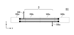
図11は、図10に示した1個のバッファ回路BCのレイアウトを拡大して示す平面図である。 FIG. 11 is an enlarged plan view showing the layout of one buffer circuit BC shown in FIG.
図11に示す例では、リードバッファ回路RBを構成する2つのエリアRBa,RBbと、ライトバッファ回路WBを構成する2つのエリアWBa,WBbの合計4エリアがX方向にこの順に並べて配置されている。図11に示すY方向に延在する配線は第2配線層L2を用いた配線であり、X方向に延在する配線は第3配線層L3を用いた配線である。つまり、図9に示した例と同様、Y方向に延在するデータバスDB及びDBaは第2配線層L2が用いられ、リードバッファ回路RBとライトバッファ回路WBとを接続する接続配線は第3配線層L3が用いられる。 In the example shown in FIG. 11, a total of four areas of two areas RBa and RBb constituting the read buffer circuit RB and two areas WBa and WBb constituting the write buffer circuit WB are arranged in this order in the X direction. . The wiring extending in the Y direction shown in FIG. 11 is a wiring using the second wiring layer L2, and the wiring extending in the X direction is a wiring using the third wiring layer L3. That is, as in the example shown in FIG. 9, the second wiring layer L2 is used for the data buses DB and DBa extending in the Y direction, and the connection wiring for connecting the read buffer circuit RB and the write buffer circuit WB is the third wiring. A wiring layer L3 is used.
図12は、バッファ回路BCを構成する回路要素と4つのエリアRBa,RBb,WBa,WBbとの関係を説明するための図である。 FIG. 12 is a diagram for explaining the relationship between circuit elements constituting the buffer circuit BC and the four areas RBa, RBb, WBa, and WBb.
図12に示すように、エリアRBaは、リードバッファ回路RBを構成するリードスイッチ82及びインバータ83が配置されるエリアであり、エリアRBbは、リードバッファ回路RBを構成するトランジスタ80,81及びインバータ84が配置されるエリアである。また、エリアWBaは、ライトバッファ回路WBを構成するトランジスタ85,86及びインバータ89が配置されるエリアであり、エリアWBbは、ライトバッファ回路WBを構成するライトスイッチ87及びインバータ88が配置されるエリアである。
As shown in FIG. 12, the area RBa is an area in which the
このように、本例では、バッファ回路BCを4つのエリアに分けて配置していることから、各バッファ回路BCはX方向における幅が長く、Y方向における幅の短いレイアウトとなる。本例では、1つのバッファ回路BC上に8本のデータバスDB又はDBaがY方向に通過することになるが、上述の通り、各バッファ回路BCはX方向における幅が長いレイアウトを有していることから、データバスDB又はDBaをY方向に通過させる通過配線領域を十分に確保することが可能となる。例えば、図11に示す領域Aが通過配線領域となる。 Thus, in this example, since the buffer circuit BC is divided into four areas, each buffer circuit BC has a long width in the X direction and a short width in the Y direction. In this example, eight data buses DB or DBa pass in the Y direction on one buffer circuit BC. As described above, each buffer circuit BC has a layout with a wide width in the X direction. Therefore, it is possible to sufficiently secure a passing wiring region through which the data bus DB or DBa passes in the Y direction. For example, a region A shown in FIG. 11 is a passing wiring region.
図13は本実施形態による効果を説明するための模式図であり、(a)は従来のレイアウトを示し、(b)は本実施形態によるレイアウトを示している。 FIG. 13 is a schematic diagram for explaining the effect of the present embodiment. FIG. 13A shows a conventional layout, and FIG. 13B shows a layout according to the present embodiment.
図13(a)に示すように、従来のレイアウトではメモリセル領域40のX方向における辺に沿ってバッファ回路BCが隙間なく配置されるため、他の回路ブロックを配置することができない。これに対し、図13(b)に示すように、本実施形態によるレイアウトでは複数(例えば4個)のバッファ回路BCがY方向に並べて配置されていることから、回路ブロック領域62を介在させることが可能となる。これにより、バッファ領域61のY方向における幅はやや大きくなるが、バッファ領域61と回路ブロック領域62のY方向における幅をほぼ一致させることにより、周辺回路領域60全体としての形状を整形することができ、チップ面積の縮小に寄与する。
As shown in FIG. 13A, in the conventional layout, since the buffer circuit BC is arranged without a gap along the side in the X direction of the
図14は本実施形態による他の効果を説明するための模式図であり、(a)は従来のレイアウトを示し、(b)は本実施形態によるレイアウトを示している。 FIG. 14 is a schematic diagram for explaining another effect according to the present embodiment. FIG. 14A shows a conventional layout, and FIG. 14B shows a layout according to the present embodiment.
図14(a)に示すように、従来のレイアウトではメモリセル領域40のX方向における辺に沿ってバッファ回路BCが隙間なく配置されるため、バッファ回路BC上をX方向に通過する内部電源配線VL1〜VL4のうち、メモリセル領域40に最も近い内部電源配線VL1については分岐配線VL1yを任意の箇所でY方向に分岐させることができる一方で、他の内部電源配線VL2〜VL4については分岐配線VL2y〜VL4yを任意の箇所でY方向に分岐させることはできない。これは、バッファ回路BCが配置された領域には他の内部電源配線やデータバスDBがY方向に延在して配線されており、分岐配線VL2y〜VL4yをY方向に形成する余地がないからである。したがって、分岐配線VL2y〜VL4yの分岐は、非アレイ領域40aにおいてのみ可能となる。このことは、内部電源配線VL2〜VL4のレイアウトが制限される結果、内部電源配線VL2〜VL4が高抵抗化することを意味する。その様子は、拡大図である図15においてより詳細に示されており、符号Bで示す箇所において分岐配線VL2y〜VL4yを接続することはできない。
As shown in FIG. 14A, in the conventional layout, the buffer circuit BC is arranged without a gap along the side in the X direction of the
これに対し、図14(b)に示すように、本実施形態によるレイアウトでは、非アレイ領域40aに対応する部分以外にも回路ブロック領域62を分散配置することができるため、分岐配線VL1y〜VL4yを高密度に配置することが可能となる。これにより、内部電源配線VL1〜VL4低抵抗化することが可能となる。その様子は、拡大図である図16においてより詳細に示されており、符号Cで示す箇所において分岐配線VL2y〜VL4yを接続することが可能となる。
On the other hand, as shown in FIG. 14B, in the layout according to the present embodiment, the
図17は本実施形態によるさらに他の効果を説明するための模式図であり、(a)は従来のレイアウトを示し、(b)は本実施形態によるレイアウトを示している。 FIG. 17 is a schematic diagram for explaining still another effect according to the present embodiment. FIG. 17A shows a conventional layout, and FIG. 17B shows a layout according to the present embodiment.
図17(a)に示すように、従来のレイアウトでは回路ブロック領域62と非アレイ領域40aのX方向における位置が一致していることから、回路ブロック領域62にて生成された内部電圧をメモリセルアレイ11に供給するためには、電源回路PWから例えばルートR1を経由する必要があり、電源配線が高抵抗化するという問題がある。これに対し、本実施形態によるレイアウトでは、図17(b)に示すように任意の位置に回路ブロック領域62を配置することができるため、電源回路PWから例えばルートR2を経由して最短距離で内部電圧を供給することが可能となる。これにより電源配線が低抵抗化することから、安定した内部電圧の供給が可能となる。しかも、電源回路PWを分散して多数配置することができるため、電源回路PWを構成するトランジスタなどの素子サイズを縮小することも可能となる。
As shown in FIG. 17A, in the conventional layout, the
図18は本実施形態によるさらに他の効果を説明するための模式図であり、(a)は従来のレイアウトを示し、(b)は本実施形態によるレイアウトを示している。 FIG. 18 is a schematic diagram for explaining still another effect according to the present embodiment. FIG. 18A shows a conventional layout, and FIG. 18B shows a layout according to the present embodiment.
図18(a)に示すように、従来のレイアウトでは、メモリセルアレイ11のエリア11a,11bを制御するための制御信号を回路ブロック領域62内の制御回路CTにて生成すると、エリア11aを制御するための信号パスとエリア11bを制御するための信号パスの長さが必然的に相違してしまう。このため、エリア11aに対する制御タイミングとエリア11bに対する制御タイミングとが相違し、制御マージンが減少する。これに対し、本実施形態によるレイアウトでは、図18(b)に示すように、エリア11aを制御するための信号パスとエリア11bを制御するための信号パスの長さが一致するよう、制御回路CTの位置を選択することができる。このため、エリア11aに対する制御タイミングとエリア11bに対する制御タイミングとを一致させることができ、制御マージンが拡大する。
As shown in FIG. 18A, in the conventional layout, when a control signal for controlling the
さらに、図19に示すように、本実施形態ではエリア11aを制御するための制御回路CTとエリア11bを制御するための制御回路CTに分けることも可能であり、この場合には、エリア11aとエリア11bとで異なる制御を行うことが可能となる。異なる制御の一例としては、エリア11aを活性化しつつエリア11bに対する電源供給を停止することで消費電流を削減したり、エリア11aに対する制御タイミングとエリア11bに対する制御タイミングとを任意にずらしたりすることが考えられる。
Furthermore, as shown in FIG. 19, in this embodiment, it is possible to divide into a control circuit CT for controlling the
図20は本実施形態によるさらに他の効果を説明するための模式図であり、(a)は従来のレイアウトを示し、(b)は本実施形態によるレイアウトを示している。 20A and 20B are schematic diagrams for explaining still another effect according to the present embodiment. FIG. 20A shows a conventional layout, and FIG. 20B shows a layout according to the present embodiment.
図20(a)に示すように、従来のレイアウトでは、制御信号のバッファリングを回路ブロック領域62内のバッファBにて行う場合、バッファBの数が大きく制限される。これに対し、本実施形態によるレイアウトでは、図20(b)に示すように、多数のバッファBを分散配置することができるため、伝送スピードを高速化することが可能であるとともに、設計により伝送スピードを細かく調整することが可能となる。
As shown in FIG. 20A, in the conventional layout, when the buffering of the control signal is performed by the buffer B in the
以上、本発明の好ましい実施形態について説明したが、本発明は、上記の実施形態に限定されることなく、本発明の主旨を逸脱しない範囲で種々の変更が可能であり、それらも本発明の範囲内に包含されるものであることはいうまでもない。 The preferred embodiments of the present invention have been described above, but the present invention is not limited to the above-described embodiments, and various modifications can be made without departing from the spirit of the present invention. Needless to say, it is included in the range.
10 半導体装置
11 メモリセルアレイ
12 ロウデコーダ
13 カラムデコーダ
14 センス回路
15 アンプ回路
20 アクセス制御回路
21 アドレス端子
22 コマンド端子
23 データ端子
30 電源回路
31,32 電源端子
40 メモリセル領域
40a 非アレイ領域
40x メモリセル領域の辺
50 パッド領域
60 周辺回路領域
61 バッファ領域
62 回路ブロック領域
63 スペース
70 ピッチ変換領域
BC バッファ回路
DB データバス
RB リードバッファ回路
VL1〜VL4 内部電源配線
VL1y〜VL4y 分岐配線
WB ライトバッファ回路
DESCRIPTION OF
Claims (12)
前記メモリセル領域の前記第2の方向に延在する辺に沿って配置され、対応する前記複数のデータバスにそれぞれ接続された複数のバッファ回路が設けられたバッファ領域と、を備え、
前記バッファ領域上においては、前記第1の方向に延在する前記複数のデータバスが第2のピッチで前記第2の方向に配列され、前記第2のピッチは前記第1のピッチよりも小さいことを特徴とする半導体装置。 A memory cell region in which a plurality of data buses extending in a first direction are arranged in a second direction at a first pitch;
A buffer region provided along a side extending in the second direction of the memory cell region, and provided with a plurality of buffer circuits respectively connected to the corresponding plurality of data buses,
On the buffer area, the plurality of data buses extending in the first direction are arranged in the second direction at a second pitch, and the second pitch is smaller than the first pitch. A semiconductor device.
前記第1のバッファ回路が形成された領域上には、前記第2のデータバスを前記第1の方向に通過させる通過配線領域が設けられており、前記第2のバッファ回路は前記通過配線領域を通過した前記第2のデータバスに接続されている、ことを特徴とする請求項9に記載の半導体装置。 The first and second buffer circuits are connected to first and second data buses included in the plurality of data buses, respectively.
On the region where the first buffer circuit is formed, a pass-through wiring region for passing the second data bus in the first direction is provided, and the second buffer circuit is provided in the pass-through wiring region. The semiconductor device according to claim 9, wherein the semiconductor device is connected to the second data bus that has passed through.
前記バッファ回路は、前記第1及び第2の電源配線間に配置された第1の回路部分と、前記第2及び第3の電源配線間に配置された第2の回路部分と、前記第2の電源配線と交差して前記第2の方向に延在し、前記第1の回路部分と前記第2の回路部分とを接続する接続配線とを含むことを特徴とする請求項1乃至10のいずれか一項に記載の半導体装置。 The buffer region is provided with first to third power supply wirings extending in the first direction,
The buffer circuit includes a first circuit portion disposed between the first and second power supply wires, a second circuit portion disposed between the second and third power supply wires, and the second circuit portion. 11. The wiring according to claim 1, further comprising a connection wiring extending in the second direction so as to intersect the power supply wiring and connecting the first circuit portion and the second circuit portion. The semiconductor device as described in any one.
Priority Applications (2)
| Application Number | Priority Date | Filing Date | Title |
|---|---|---|---|
| JP2011068358A JP2012204643A (en) | 2011-03-25 | 2011-03-25 | Semiconductor device |
| US13/420,105 US8848460B2 (en) | 2011-03-25 | 2012-03-14 | Semiconductor device having plural data buses and plural buffer circuits connected to data buses |
Applications Claiming Priority (1)
| Application Number | Priority Date | Filing Date | Title |
|---|---|---|---|
| JP2011068358A JP2012204643A (en) | 2011-03-25 | 2011-03-25 | Semiconductor device |
Publications (1)
| Publication Number | Publication Date |
|---|---|
| JP2012204643A true JP2012204643A (en) | 2012-10-22 |
Family
ID=46877255
Family Applications (1)
| Application Number | Title | Priority Date | Filing Date |
|---|---|---|---|
| JP2011068358A Ceased JP2012204643A (en) | 2011-03-25 | 2011-03-25 | Semiconductor device |
Country Status (2)
| Country | Link |
|---|---|
| US (1) | US8848460B2 (en) |
| JP (1) | JP2012204643A (en) |
Cited By (1)
| Publication number | Priority date | Publication date | Assignee | Title |
|---|---|---|---|---|
| CN114078489A (en) * | 2020-08-17 | 2022-02-22 | 铠侠股份有限公司 | Semiconductor memory device with a plurality of memory cells |
Families Citing this family (1)
| Publication number | Priority date | Publication date | Assignee | Title |
|---|---|---|---|---|
| CN118866046B (en) * | 2023-04-14 | 2025-10-03 | 长鑫存储技术有限公司 | A memory |
Citations (7)
| Publication number | Priority date | Publication date | Assignee | Title |
|---|---|---|---|---|
| JPH08279602A (en) * | 1995-03-13 | 1996-10-22 | Toshiba Corp | Semiconductor memory device |
| JPH11177059A (en) * | 1997-12-12 | 1999-07-02 | Toshiba Corp | Semiconductor memory device |
| JP2000100169A (en) * | 1998-09-22 | 2000-04-07 | Fujitsu Ltd | Semiconductor memory device and data control method for semiconductor memory device |
| JP2000228508A (en) * | 1999-02-08 | 2000-08-15 | Toshiba Corp | Semiconductor storage device |
| JP2003086710A (en) * | 2001-09-14 | 2003-03-20 | Matsushita Electric Ind Co Ltd | Semiconductor memory device |
| JP2006121097A (en) * | 2005-11-09 | 2006-05-11 | Hitachi Ltd | Semiconductor integrated circuit device |
| JP2006253270A (en) * | 2005-03-09 | 2006-09-21 | Elpida Memory Inc | Semiconductor memory device |
Family Cites Families (5)
| Publication number | Priority date | Publication date | Assignee | Title |
|---|---|---|---|---|
| JPH0642536B2 (en) * | 1985-08-16 | 1994-06-01 | 富士通株式会社 | Semiconductor memory device |
| US5835440A (en) * | 1997-08-06 | 1998-11-10 | Micron Technology, Inc. | Memory device equilibration circuit and method |
| US6130843A (en) * | 1998-09-02 | 2000-10-10 | Micron Technology, Inc. | Method and circuit for providing a memory device having hidden row access and row precharge times |
| US6768338B1 (en) * | 2003-01-30 | 2004-07-27 | Xilinx, Inc. | PLD lookup table including transistors of more than one oxide thickness |
| JP2011061091A (en) * | 2009-09-11 | 2011-03-24 | Toshiba Corp | Semiconductor memory device |
-
2011
- 2011-03-25 JP JP2011068358A patent/JP2012204643A/en not_active Ceased
-
2012
- 2012-03-14 US US13/420,105 patent/US8848460B2/en active Active
Patent Citations (7)
| Publication number | Priority date | Publication date | Assignee | Title |
|---|---|---|---|---|
| JPH08279602A (en) * | 1995-03-13 | 1996-10-22 | Toshiba Corp | Semiconductor memory device |
| JPH11177059A (en) * | 1997-12-12 | 1999-07-02 | Toshiba Corp | Semiconductor memory device |
| JP2000100169A (en) * | 1998-09-22 | 2000-04-07 | Fujitsu Ltd | Semiconductor memory device and data control method for semiconductor memory device |
| JP2000228508A (en) * | 1999-02-08 | 2000-08-15 | Toshiba Corp | Semiconductor storage device |
| JP2003086710A (en) * | 2001-09-14 | 2003-03-20 | Matsushita Electric Ind Co Ltd | Semiconductor memory device |
| JP2006253270A (en) * | 2005-03-09 | 2006-09-21 | Elpida Memory Inc | Semiconductor memory device |
| JP2006121097A (en) * | 2005-11-09 | 2006-05-11 | Hitachi Ltd | Semiconductor integrated circuit device |
Cited By (4)
| Publication number | Priority date | Publication date | Assignee | Title |
|---|---|---|---|---|
| CN114078489A (en) * | 2020-08-17 | 2022-02-22 | 铠侠股份有限公司 | Semiconductor memory device with a plurality of memory cells |
| JP2022033615A (en) * | 2020-08-17 | 2022-03-02 | キオクシア株式会社 | Semiconductor memory device |
| JP7467278B2 (en) | 2020-08-17 | 2024-04-15 | キオクシア株式会社 | Semiconductor memory device |
| CN114078489B (en) * | 2020-08-17 | 2025-07-25 | 铠侠股份有限公司 | Semiconductor memory device with a memory cell having a memory cell with a memory cell having a memory cell |
Also Published As
| Publication number | Publication date |
|---|---|
| US8848460B2 (en) | 2014-09-30 |
| US20120243341A1 (en) | 2012-09-27 |
Similar Documents
| Publication | Publication Date | Title |
|---|---|---|
| JP4056107B2 (en) | Semiconductor integrated circuit | |
| US8806411B2 (en) | Semiconductor device based on power gating in multilevel wiring structure | |
| US9240221B2 (en) | Semiconductor memory device with a selection transistor having same shape and size as a memory cell transistor | |
| JP2015032651A (en) | Semiconductor device | |
| JP3902389B2 (en) | Static random access memory with global bit lines | |
| US7773405B2 (en) | Magnetic random access memory and operating method of magnetic random access memory | |
| JP3996267B2 (en) | Semiconductor memory device | |
| JPH11354758A (en) | Semiconductor storage device | |
| JP3938803B2 (en) | Dynamic RAM | |
| JP2003007852A (en) | Semiconductor storage device | |
| JP2012204643A (en) | Semiconductor device | |
| JP6029434B2 (en) | Semiconductor memory device | |
| JP2013191262A (en) | Semiconductor device | |
| WO2017145312A1 (en) | Semiconductor storage device | |
| US8674411B2 (en) | Semiconductor device employing circuit blocks having the same characteristics | |
| JP2010074023A (en) | Semiconductor device | |
| JP2009272587A (en) | Semiconductor storage device | |
| JP2009038306A (en) | Semiconductor memory device | |
| KR20010111007A (en) | Semiconductor memory device having segment type word line structure | |
| JP4600835B2 (en) | Semiconductor integrated circuit | |
| JP7411531B2 (en) | semiconductor equipment | |
| JP2002203391A (en) | Semiconductor memory and arrangement method for distributed driver | |
| JP6618587B2 (en) | Semiconductor device | |
| JP2006277889A (en) | Semiconductor memory device | |
| US8767484B2 (en) | Semiconductor device |
Legal Events
| Date | Code | Title | Description |
|---|---|---|---|
| A711 | Notification of change in applicant |
Free format text: JAPANESE INTERMEDIATE CODE: A711 Effective date: 20130730 |
|
| A521 | Request for written amendment filed |
Free format text: JAPANESE INTERMEDIATE CODE: A523 Effective date: 20130822 |
|
| A621 | Written request for application examination |
Free format text: JAPANESE INTERMEDIATE CODE: A621 Effective date: 20140306 |
|
| A977 | Report on retrieval |
Free format text: JAPANESE INTERMEDIATE CODE: A971007 Effective date: 20141218 |
|
| A131 | Notification of reasons for refusal |
Free format text: JAPANESE INTERMEDIATE CODE: A131 Effective date: 20150106 |
|
| A601 | Written request for extension of time |
Free format text: JAPANESE INTERMEDIATE CODE: A601 Effective date: 20150403 |
|
| A601 | Written request for extension of time |
Free format text: JAPANESE INTERMEDIATE CODE: A601 Effective date: 20150501 |
|
| A601 | Written request for extension of time |
Free format text: JAPANESE INTERMEDIATE CODE: A601 Effective date: 20150602 |
|
| A01 | Written decision to grant a patent or to grant a registration (utility model) |
Free format text: JAPANESE INTERMEDIATE CODE: A01 Effective date: 20151027 |
|
| A045 | Written measure of dismissal of application [lapsed due to lack of payment] |
Free format text: JAPANESE INTERMEDIATE CODE: A045 Effective date: 20160223 |