JP2012208302A - 液晶装置および投射型表示装置 - Google Patents
液晶装置および投射型表示装置 Download PDFInfo
- Publication number
- JP2012208302A JP2012208302A JP2011073576A JP2011073576A JP2012208302A JP 2012208302 A JP2012208302 A JP 2012208302A JP 2011073576 A JP2011073576 A JP 2011073576A JP 2011073576 A JP2011073576 A JP 2011073576A JP 2012208302 A JP2012208302 A JP 2012208302A
- Authority
- JP
- Japan
- Prior art keywords
- liquid crystal
- image display
- driving circuit
- line driving
- crystal device
- Prior art date
- Legal status (The legal status is an assumption and is not a legal conclusion. Google has not performed a legal analysis and makes no representation as to the accuracy of the status listed.)
- Granted
Links
Images





Classifications
-
- G—PHYSICS
- G02—OPTICS
- G02F—OPTICAL DEVICES OR ARRANGEMENTS FOR THE CONTROL OF LIGHT BY MODIFICATION OF THE OPTICAL PROPERTIES OF THE MEDIA OF THE ELEMENTS INVOLVED THEREIN; NON-LINEAR OPTICS; FREQUENCY-CHANGING OF LIGHT; OPTICAL LOGIC ELEMENTS; OPTICAL ANALOGUE/DIGITAL CONVERTERS
- G02F1/00—Devices or arrangements for the control of the intensity, colour, phase, polarisation or direction of light arriving from an independent light source, e.g. switching, gating or modulating; Non-linear optics
- G02F1/01—Devices or arrangements for the control of the intensity, colour, phase, polarisation or direction of light arriving from an independent light source, e.g. switching, gating or modulating; Non-linear optics for the control of the intensity, phase, polarisation or colour
- G02F1/13—Devices or arrangements for the control of the intensity, colour, phase, polarisation or direction of light arriving from an independent light source, e.g. switching, gating or modulating; Non-linear optics for the control of the intensity, phase, polarisation or colour based on liquid crystals, e.g. single liquid crystal display cells
- G02F1/133—Constructional arrangements; Operation of liquid crystal cells; Circuit arrangements
- G02F1/1333—Constructional arrangements; Manufacturing methods
- G02F1/1341—Filling or closing of cells
-
- G—PHYSICS
- G02—OPTICS
- G02F—OPTICAL DEVICES OR ARRANGEMENTS FOR THE CONTROL OF LIGHT BY MODIFICATION OF THE OPTICAL PROPERTIES OF THE MEDIA OF THE ELEMENTS INVOLVED THEREIN; NON-LINEAR OPTICS; FREQUENCY-CHANGING OF LIGHT; OPTICAL LOGIC ELEMENTS; OPTICAL ANALOGUE/DIGITAL CONVERTERS
- G02F1/00—Devices or arrangements for the control of the intensity, colour, phase, polarisation or direction of light arriving from an independent light source, e.g. switching, gating or modulating; Non-linear optics
- G02F1/01—Devices or arrangements for the control of the intensity, colour, phase, polarisation or direction of light arriving from an independent light source, e.g. switching, gating or modulating; Non-linear optics for the control of the intensity, phase, polarisation or colour
- G02F1/13—Devices or arrangements for the control of the intensity, colour, phase, polarisation or direction of light arriving from an independent light source, e.g. switching, gating or modulating; Non-linear optics for the control of the intensity, phase, polarisation or colour based on liquid crystals, e.g. single liquid crystal display cells
- G02F1/133—Constructional arrangements; Operation of liquid crystal cells; Circuit arrangements
- G02F1/1333—Constructional arrangements; Manufacturing methods
- G02F1/1345—Conductors connecting electrodes to cell terminals
- G02F1/13452—Conductors connecting driver circuitry and terminals of panels
-
- G—PHYSICS
- G02—OPTICS
- G02F—OPTICAL DEVICES OR ARRANGEMENTS FOR THE CONTROL OF LIGHT BY MODIFICATION OF THE OPTICAL PROPERTIES OF THE MEDIA OF THE ELEMENTS INVOLVED THEREIN; NON-LINEAR OPTICS; FREQUENCY-CHANGING OF LIGHT; OPTICAL LOGIC ELEMENTS; OPTICAL ANALOGUE/DIGITAL CONVERTERS
- G02F1/00—Devices or arrangements for the control of the intensity, colour, phase, polarisation or direction of light arriving from an independent light source, e.g. switching, gating or modulating; Non-linear optics
- G02F1/01—Devices or arrangements for the control of the intensity, colour, phase, polarisation or direction of light arriving from an independent light source, e.g. switching, gating or modulating; Non-linear optics for the control of the intensity, phase, polarisation or colour
- G02F1/13—Devices or arrangements for the control of the intensity, colour, phase, polarisation or direction of light arriving from an independent light source, e.g. switching, gating or modulating; Non-linear optics for the control of the intensity, phase, polarisation or colour based on liquid crystals, e.g. single liquid crystal display cells
- G02F1/133—Constructional arrangements; Operation of liquid crystal cells; Circuit arrangements
- G02F1/136—Liquid crystal cells structurally associated with a semi-conducting layer or substrate, e.g. cells forming part of an integrated circuit
- G02F1/1362—Active matrix addressed cells
- G02F1/136286—Wiring, e.g. gate line, drain line
-
- G—PHYSICS
- G09—EDUCATION; CRYPTOGRAPHY; DISPLAY; ADVERTISING; SEALS
- G09G—ARRANGEMENTS OR CIRCUITS FOR CONTROL OF INDICATING DEVICES USING STATIC MEANS TO PRESENT VARIABLE INFORMATION
- G09G3/00—Control arrangements or circuits, of interest only in connection with visual indicators other than cathode-ray tubes
- G09G3/001—Control arrangements or circuits, of interest only in connection with visual indicators other than cathode-ray tubes using specific devices not provided for in groups G09G3/02 - G09G3/36, e.g. using an intermediate record carrier such as a film slide; Projection systems; Display of non-alphanumerical information, solely or in combination with alphanumerical information, e.g. digital display on projected diapositive as background
- G09G3/002—Control arrangements or circuits, of interest only in connection with visual indicators other than cathode-ray tubes using specific devices not provided for in groups G09G3/02 - G09G3/36, e.g. using an intermediate record carrier such as a film slide; Projection systems; Display of non-alphanumerical information, solely or in combination with alphanumerical information, e.g. digital display on projected diapositive as background to project the image of a two-dimensional display, such as an array of light emitting or modulating elements or a CRT
-
- G—PHYSICS
- G09—EDUCATION; CRYPTOGRAPHY; DISPLAY; ADVERTISING; SEALS
- G09G—ARRANGEMENTS OR CIRCUITS FOR CONTROL OF INDICATING DEVICES USING STATIC MEANS TO PRESENT VARIABLE INFORMATION
- G09G3/00—Control arrangements or circuits, of interest only in connection with visual indicators other than cathode-ray tubes
- G09G3/20—Control arrangements or circuits, of interest only in connection with visual indicators other than cathode-ray tubes for presentation of an assembly of a number of characters, e.g. a page, by composing the assembly by combination of individual elements arranged in a matrix no fixed position being assigned to or needed to be assigned to the individual characters or partial characters
- G09G3/34—Control arrangements or circuits, of interest only in connection with visual indicators other than cathode-ray tubes for presentation of an assembly of a number of characters, e.g. a page, by composing the assembly by combination of individual elements arranged in a matrix no fixed position being assigned to or needed to be assigned to the individual characters or partial characters by control of light from an independent source
- G09G3/36—Control arrangements or circuits, of interest only in connection with visual indicators other than cathode-ray tubes for presentation of an assembly of a number of characters, e.g. a page, by composing the assembly by combination of individual elements arranged in a matrix no fixed position being assigned to or needed to be assigned to the individual characters or partial characters by control of light from an independent source using liquid crystals
- G09G3/3611—Control of matrices with row and column drivers
- G09G3/3648—Control of matrices with row and column drivers using an active matrix
-
- G—PHYSICS
- G09—EDUCATION; CRYPTOGRAPHY; DISPLAY; ADVERTISING; SEALS
- G09G—ARRANGEMENTS OR CIRCUITS FOR CONTROL OF INDICATING DEVICES USING STATIC MEANS TO PRESENT VARIABLE INFORMATION
- G09G2300/00—Aspects of the constitution of display devices
- G09G2300/04—Structural and physical details of display devices
- G09G2300/0404—Matrix technologies
- G09G2300/0417—Special arrangements specific to the use of low carrier mobility technology
-
- G—PHYSICS
- G09—EDUCATION; CRYPTOGRAPHY; DISPLAY; ADVERTISING; SEALS
- G09G—ARRANGEMENTS OR CIRCUITS FOR CONTROL OF INDICATING DEVICES USING STATIC MEANS TO PRESENT VARIABLE INFORMATION
- G09G2310/00—Command of the display device
- G09G2310/02—Addressing, scanning or driving the display screen or processing steps related thereto
- G09G2310/0232—Special driving of display border areas
-
- G—PHYSICS
- G09—EDUCATION; CRYPTOGRAPHY; DISPLAY; ADVERTISING; SEALS
- G09G—ARRANGEMENTS OR CIRCUITS FOR CONTROL OF INDICATING DEVICES USING STATIC MEANS TO PRESENT VARIABLE INFORMATION
- G09G2320/00—Control of display operating conditions
- G09G2320/04—Maintaining the quality of display appearance
- G09G2320/043—Preventing or counteracting the effects of ageing
Landscapes
- Physics & Mathematics (AREA)
- Nonlinear Science (AREA)
- General Physics & Mathematics (AREA)
- Engineering & Computer Science (AREA)
- Chemical & Material Sciences (AREA)
- Crystallography & Structural Chemistry (AREA)
- Mathematical Physics (AREA)
- Optics & Photonics (AREA)
- Liquid Crystal (AREA)
- Theoretical Computer Science (AREA)
- Computer Hardware Design (AREA)
- Microelectronics & Electronic Packaging (AREA)
- Projection Apparatus (AREA)
- Devices For Indicating Variable Information By Combining Individual Elements (AREA)
Abstract
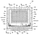
【解決手段】液晶装置100の素子基板において、画像表示領域10aとシール材107とにより挟まれた周辺領域10bには、ダミー画素電極9b等に印加される共通電位Vcomとは異なるイオン性不純物トラップ用の電位Vtrapが印加された周辺電極8aが形成されている。周辺電極8aは、データ線駆動回路部101の外側端部101b、および走査線駆動回路部104の外側端部104bの外側を通ってシール材107に沿って延在しており、データ線および走査線と交差していない。
【選択図】図3
Description
(全体構成)
図1は、本発明を適用した液晶装置の電気的構成を示すブロック図である。なお、図1は、あくまで電気的な構成を示すブロック図であり、配線や電極の形状や延在方向、レイアウト等を示しているものではない。
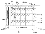
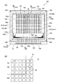
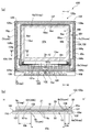
図2は、本発明の実施の形態1に係る液晶装置100の液晶パネル100pの説明図であり、図2(a)、(b)は各々、本発明を適用した液晶装置100の液晶パネル100pを各構成要素と共に対向基板の側から見た平面図、およびそのH−H′断面図である。図3は、本発明の実施の形態1に係る液晶装置100の素子基板10に形成されている電極等の説明図であり、図3(a)、(b)は各々、素子基板10全体における画素電極9aやダミー画素電極9bのレイアウトを示す説明図、およびダミー画素電極9bの形状等を示す説明図である。なお、図3および図4においては画素電極9aやダミー画素電極9bの数等について少なく示してある。
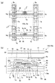
図4は、本発明の実施の形態1に係る液晶装置100の画素の説明図であり、図4(a)、(b)は各々、本発明を適用した液晶装置100に用いた素子基板10において隣り合う画素の平面図、および図4(a)のF−F′線に相当する位置で液晶装置100を切断したときの断面図である。なお、図4(a)では、半導体層は細くて短い点線で示し、走査線3aは太い実線で示し、データ線6aおよびそれと同時形成された薄膜は一点鎖線で示し、容量線5bは二点鎖線で示し、画素電極9aは太くて長い点線で示し、ドレイン電極4aは細い実線で示してある。なお、走査線3aや容量線5b等と重なる領域には遮光層7aが形成されているが、図4(a)では遮光層7aの図示を省略してある。
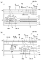
図5は、本発明の実施の形態1に係る液晶装置100の周辺領域10bの断面構成を模式的に示す説明図であり、図5(a)、(b)は、図2のV−V′線に相当する位置での断面図、および図2のG−G′線に相当する位置での断面図である。図5に示すように、液晶装置100では、図1および図2を参照して説明したデータ線駆動回路部101および走査線駆動回路部104等の周辺回路部106には、nチャネル型やpチャネル型の駆動用トランジスター106aを備えた相補型トランジスター回路等が構成されている。また、周辺回路部106には各種の配線106c等も形成されている。ここで、駆動用トランジスター106aは、画素トランジスター30の製造工程の一部を利用して形成されたものであるため、素子基板10においてデータ線駆動回路部101および走査線駆動回路部104が形成されている領域も、図3(b)に示す断面構成と略同様な断面構成を有している。
図2、図3および図5に示すように、本形態の液晶装置100の素子基板10において、画像表示領域10aとシール材107とにより挟まれた周辺領域10bには、ダミー画素電極9bより外周側にイオン性不純物トラップ用の周辺電極8aが形成されている。本形態において、周辺電極8aは、ITOやIZO等の導電性金属酸化膜、導電性のポリシリコン膜、金属シリサイド膜、金属膜等からなる。かかる周辺電極8aは、周辺回路部106およびダミー画素電極9bの空き領域等を利用して、図1、図2(a)および図3(a)に示す配線5sに電気的に接続されている。かかる周辺電極8aと配線5sとの電気的な接続には、図5(a)、(b)に示すように、第3層間絶縁膜44に形成したコンタクトホール44c、44dや、中継電極6e、6fが利用される。
以上説明したように、本形態の液晶装置100において、素子基板10の周辺領域10bには、共通電位Vcomと異なる電位Vtrapが印加された周辺電極8aが設けられているため、イオン性不純物が画像表示領域10aで凝集しないので、イオン性不純物に起因する表示品位の低下を防止することができる。特にVAモードの液晶装置100の場合、液晶分子が垂直姿勢と水平に平伏した姿勢とに切り換わる際の流動によって、プレチルトの方位に対応する対角の角領域イオン性不純物が偏在しやすいが、本形態では、周辺電極8aによって、イオン性不純物を効果的にトラップすることができる。また、配向膜16、26として無機配向膜を用いた場合、無機配向膜は、イオン性不純物を吸着しやすい傾向にあるが、本形態では、周辺電極8aによって、イオン性不純物を効果的にトラップすることができる。それ故、VAモードの液晶装置100において無機配向膜を用いた場合でも、画像表示領域10aでイオン性不純物が凝集することを確実に防止することができる。
図6は、本発明の実施の形態2に係る液晶装置100の液晶パネル100pの説明図であり、図6(a)、(b)は各々、本発明を適用した液晶装置100の液晶パネル100pを各構成要素と共に対向基板の側から見た平面図、およびそのH−H′断面図である。図7は、本発明の実施の形態2に係る液晶装置100の素子基板10に形成されている電極等の説明図である。図8は、本発明の実施の形態2に係る液晶装置100の周辺領域10bの断面構成を模式的に示す説明図であり、図8(a)、(b)は、図6のV−V′線に相当する位置での断面図、および図6のG−G′線に相当する位置での断面図である。なお、本形態の基本的な構成は実施の形態1と同様であるため、共通する部分には同一の符号を付してそれらの説明を省略する。
図9は、本発明の実施の形態3に係る液晶装置100の液晶パネル100pの説明図であり、図9(a)、(b)は各々、本発明を適用した液晶装置100の液晶パネル100pを各構成要素と共に対向基板の側から見た平面図、およびそのH−H′断面図である。図10は、本発明の実施の形態3に係る液晶装置100の素子基板10に形成されている電極等の説明図である。図11は、本発明の実施の形態3に係る液晶装置100の周辺領域10bの断面構成を模式的に示す説明図であり、図11(a)、(b)は、図9のV−V′線に相当する位置での断面図、および図9のG−G′線に相当する位置での断面図である。なお、本形態の基本的な構成は実施の形態1と同様であるため、共通する部分には同一の符号を付してそれらの説明を省略する。
図12は、本発明の実施の形態4に係る液晶装置100の周辺領域10bの断面構成を示す説明図であり、図2のV−V′線に相当する位置での断面図、および図2のG−G′線に相当する位置での断面図である。なお、本形態の基本的な構成は実施の形態1と同様であるため、共通する部分には同一の符号を付してそれらの説明を省略する。
上記実施の形態において、周辺電極8aは、全周で繋がった構成になっていたが、イオン性不純物トラップ用の電位Vtrapを印加可能な構成であれば、周辺電極8aが部分的に途切れていてもよい。また、上記実施の形態において、周辺電極8aは、1列のみ形成されていたが、周辺電極8aが複数列に形成されていてもよい。この場合、複数の周辺電極8aにおいて、異なるイオン性不純物トラップ用の電位Vtrapを印加してもよい。
上述した実施形態に係る液晶装置100を適用した電子機器について説明する。図13は、本発明を適用した液晶装置100を用いた投射型表示装置の概略構成図であり、図13(a)、(b)は各々、透過型の液晶装置100を用いた投射型表示装置の説明図、および反射型の液晶装置100を用いた投射型表示装置の説明図である。
図13(a)に示す投射型表示装置110は、観察者側に設けられたスクリーン111に光を照射し、このスクリーン111で反射した光を観察する、いわゆる投影型の投射型表示装置である。投射型表示装置110は、光源112を備えた光源部130と、ダイクロイックミラー113、114と、液晶ライトバルブ115〜117(液晶装置100)と、投射光学系118と、クロスダイクロイックプリズム119と、リレー系120とを備えている。
図13(b)に示す投射型表示装置1000は、光源光を発生する光源部1021と、光源部1021から出射された光源光を赤、緑、青の3色に分離する色分離導光光学系1023と、色分離導光光学系1023から出射された各色の光源光によって照明される光変調部1025とを有している。また、投射型表示装置1000は、光変調部1025から出射された各色の像光を合成するクロスダイクロイックプリズム1027(合成光学系)と、クロスダイクロイックプリズム1027を経た像光をスクリーン(不図示)に投射するための投射光学系である投射光学系1029とを備えている。
なお、投射型表示装置については、光源部として、各色の光を出射するLED光源等を用い、かかるLED光源から出射された色光を各々、別の液晶装置に供給するように構成してもよい。
本発明を適用した液晶装置100については、上記の電子機器の他にも、携帯電話機、情報携帯端末(PDA:Personal Digital Assistants)、デジタルカメラ、液晶テレビ、カーナビゲーション装置、テレビ電話、POS端末、タッチパネルを備えた機器等の電子機器において直視型表示装置として用いてもよい。
Claims (7)
- 一方面側に複数の画素電極が配列する画像表示領域が設けられた素子基板と、
共通電位が印加される共通電極が設けられた対向基板と、
前記素子基板と前記対向基板とを貼り合わすシール材と、
前記素子基板と前記対向基板との間において前記シール材で囲まれた領域内に保持された液晶層と、
を有し、
前記素子基板の前記一方面側には、
前記画像表示領域の第1端部に沿って設けられ、当該第1端部と前記素子基板の第1辺との間に配置されたデータ線駆動回路部と、
該データ線駆動回路部の前記画像表示領域側に位置する端部から前記画像表示領域内に向けて延在する複数のデータ線と、
前記画像表示領域において前記第1端部に交差する第2端部に沿って設けられ、前記素子基板の前記第1辺と交差する第2辺と前記第2端部との間に配置された走査線駆動回路部と、
該走査線駆動回路部の前記画像表示領域側に位置する端部から前記画像表示領域内に向けて延在する複数の走査線と、
前記画像表示領域と前記シール材との間において、前記データ線駆動回路部の前記画像表示領域側の端部と前記第1辺との間、および前記走査線駆動回路部の前記画像表示領域側の端部と前記第2辺との間のうちの少なくとも一方を通って前記シール材に沿うように延在し、前記共通電位と異なる電位が印加された周辺電極と、
が設けられていることを特徴とする液晶装置。 - 前記周辺電極は、前記データ線駆動回路部の前記第1辺側の端部と当該第1辺との間、および前記走査線駆動回路部の前記第2辺側の端部と当該第2辺との間のうちの少なくとも一方を通って前記シール材に沿うように延在していることを特徴とする請求項1に記載の液晶装置。
- 前記周辺電極は、前記データ線駆動回路部の前記画像表示領域側の端部と前記第1辺との間、および前記走査線駆動回路部の前記画像表示領域側の端部と前記第2辺との間の双方を通って前記シール材に沿うように延在していることを特徴とする請求項1または2に記載の液晶装置。
- 前記周辺電極は、少なくとも前記走査線駆動回路部の前記画像表示領域側の端部と前記第2辺との間を通って前記シール材に沿うように延在していることを特徴とする請求項1または2に記載の液晶装置。
- 前記周辺電極は、少なくとも前記データ線駆動回路部の前記画像表示領域側の端部と前記第1辺との間を通って前記シール材に沿うように延在していることを特徴とする請求項1または2に記載の液晶装置。
- 一方面側に複数の画素電極が配列する画像表示領域が設けられ、第1辺および該第1辺に交差する第2辺を有する素子基板と、
共通電位が印加される共通電極が設けられた対向基板と、
前記素子基板と前記対向基板とを貼り合わすシール材と、
前記素子基板と前記対向基板との間において前記シール材で囲まれた領域内に保持された液晶層と、
を有し、
前記画像表示領域は、前記第1辺側に位置する第1端部、および前記第2辺側に位置する第2端部を有し、
前記素子基板の前記一方面側には、
前記第1辺と前記第1端部との間に配置され、前記第1端部に沿うように設けられたデータ線駆動回路部と、
前記データ線駆動回路部から前記画像表示領域に向けて延在する複数のデータ線と、
前記第2辺と前記第2端部との間に配置され、前記第2端部に沿うように設けられた走査線駆動回路部と、
前記走査線駆動回路部から前記画像表示領域に向けて延在する複数の走査線と、
前記画像表示領域と前記シール材との間において、前記第1辺と前記複数のデータ線との間、および前記第2辺と前記複数の走査線との間のうち少なくとも一方を通って前記シール材に沿うように延在し、前記共通電位と異なる電位が印加された周辺電極と、
が設けられていることを特徴とする液晶装置。 - 請求項1乃至6の何れか一項に記載の液晶装置を備えた投射型表示装置であって、
前記液晶装置に供給される光を出射する光源部と、
前記液晶装置によって変調された光を投射する投射光学系と、
を有していることを特徴とする投射型表示装置。
Priority Applications (3)
| Application Number | Priority Date | Filing Date | Title |
|---|---|---|---|
| JP2011073576A JP5708133B2 (ja) | 2011-03-29 | 2011-03-29 | 液晶装置および投射型表示装置 |
| CN201210076045.8A CN102736326B (zh) | 2011-03-29 | 2012-03-21 | 液晶装置以及投射型显示装置 |
| US13/429,541 US8817219B2 (en) | 2011-03-29 | 2012-03-26 | Liquid crystal device and projection-type display device |
Applications Claiming Priority (1)
| Application Number | Priority Date | Filing Date | Title |
|---|---|---|---|
| JP2011073576A JP5708133B2 (ja) | 2011-03-29 | 2011-03-29 | 液晶装置および投射型表示装置 |
Publications (3)
| Publication Number | Publication Date |
|---|---|
| JP2012208302A true JP2012208302A (ja) | 2012-10-25 |
| JP2012208302A5 JP2012208302A5 (ja) | 2014-03-27 |
| JP5708133B2 JP5708133B2 (ja) | 2015-04-30 |
Family
ID=46926819
Family Applications (1)
| Application Number | Title | Priority Date | Filing Date |
|---|---|---|---|
| JP2011073576A Active JP5708133B2 (ja) | 2011-03-29 | 2011-03-29 | 液晶装置および投射型表示装置 |
Country Status (3)
| Country | Link |
|---|---|
| US (1) | US8817219B2 (ja) |
| JP (1) | JP5708133B2 (ja) |
| CN (1) | CN102736326B (ja) |
Families Citing this family (9)
| Publication number | Priority date | Publication date | Assignee | Title |
|---|---|---|---|---|
| CN104280954B (zh) * | 2014-08-06 | 2017-02-08 | 深圳市华星光电技术有限公司 | 一种液晶显示器及其液晶显示器下基板组件 |
| JP6475947B2 (ja) * | 2014-09-30 | 2019-02-27 | 株式会社ジャパンディスプレイ | 液晶表示装置 |
| KR102544696B1 (ko) * | 2015-02-16 | 2023-06-16 | 삼성디스플레이 주식회사 | 원형 터치 패널 및 그 제조 방법 |
| KR20170002789A (ko) * | 2015-06-29 | 2017-01-09 | 삼성디스플레이 주식회사 | 액정 표시 장치 |
| CN105097557A (zh) * | 2015-09-25 | 2015-11-25 | 深圳市华星光电技术有限公司 | 一种tft基板、tft开关管及其制造方法 |
| KR102656664B1 (ko) * | 2016-10-06 | 2024-04-12 | 삼성디스플레이 주식회사 | 표시장치 |
| US10108053B2 (en) * | 2016-10-21 | 2018-10-23 | Omnivision Technologies, Inc. | Liquid crystal display device with peripheral electrode |
| CN112764281B (zh) * | 2021-01-28 | 2021-11-23 | Tcl华星光电技术有限公司 | 一种阵列基板及显示面板 |
| JP7703884B2 (ja) * | 2021-04-22 | 2025-07-08 | セイコーエプソン株式会社 | 電気光学装置および電子機器 |
Citations (3)
| Publication number | Priority date | Publication date | Assignee | Title |
|---|---|---|---|---|
| JPH1039326A (ja) * | 1996-07-29 | 1998-02-13 | Matsushita Electron Corp | 薄膜トランジスタ液晶表示装置 |
| JPH10268358A (ja) * | 1997-03-21 | 1998-10-09 | Victor Co Of Japan Ltd | 液晶画像表示装置及びその製造方法 |
| JP2005078048A (ja) * | 2003-09-04 | 2005-03-24 | Sharp Corp | アクティブマトリクス基板、アクティブマトリクス基板の製造方法、および液晶表示装置 |
Family Cites Families (13)
| Publication number | Priority date | Publication date | Assignee | Title |
|---|---|---|---|---|
| JP2687704B2 (ja) | 1990-09-18 | 1997-12-08 | トヨタ自動車株式会社 | サスペンション制御装置 |
| JPH06289408A (ja) | 1993-03-30 | 1994-10-18 | Seiko Instr Inc | 液晶表示装置 |
| JP3883641B2 (ja) * | 1997-03-27 | 2007-02-21 | 株式会社半導体エネルギー研究所 | コンタクト構造およびアクティブマトリクス型表示装置 |
| JP3497098B2 (ja) * | 1999-05-25 | 2004-02-16 | シャープ株式会社 | 液晶表示素子 |
| CN1209662C (zh) * | 2001-12-17 | 2005-07-06 | 精工爱普生株式会社 | 显示装置及电子机器 |
| CN100578321C (zh) * | 2005-03-15 | 2010-01-06 | 富士通株式会社 | 液晶显示装置及配向处理方法 |
| JP4923866B2 (ja) * | 2006-08-30 | 2012-04-25 | ソニー株式会社 | 液晶表示装置および映像表示装置 |
| JP2008164787A (ja) * | 2006-12-27 | 2008-07-17 | Epson Imaging Devices Corp | 液晶表示装置 |
| JP4379507B2 (ja) * | 2007-09-05 | 2009-12-09 | ソニー株式会社 | 液晶表示装置および液晶パネル |
| JP2009092697A (ja) | 2007-10-03 | 2009-04-30 | Sony Corp | 液晶表示装置及び映像表示装置 |
| CN101825817B (zh) * | 2009-03-06 | 2011-12-14 | 北京京东方光电科技有限公司 | 一种液晶显示器 |
| WO2010131503A1 (ja) * | 2009-05-15 | 2010-11-18 | シャープ株式会社 | 表示パネルおよびそれを備えた表示装置 |
| KR101097333B1 (ko) * | 2010-02-11 | 2011-12-23 | 삼성모바일디스플레이주식회사 | 액정표시장치 |
-
2011
- 2011-03-29 JP JP2011073576A patent/JP5708133B2/ja active Active
-
2012
- 2012-03-21 CN CN201210076045.8A patent/CN102736326B/zh active Active
- 2012-03-26 US US13/429,541 patent/US8817219B2/en active Active
Patent Citations (3)
| Publication number | Priority date | Publication date | Assignee | Title |
|---|---|---|---|---|
| JPH1039326A (ja) * | 1996-07-29 | 1998-02-13 | Matsushita Electron Corp | 薄膜トランジスタ液晶表示装置 |
| JPH10268358A (ja) * | 1997-03-21 | 1998-10-09 | Victor Co Of Japan Ltd | 液晶画像表示装置及びその製造方法 |
| JP2005078048A (ja) * | 2003-09-04 | 2005-03-24 | Sharp Corp | アクティブマトリクス基板、アクティブマトリクス基板の製造方法、および液晶表示装置 |
Also Published As
| Publication number | Publication date |
|---|---|
| US8817219B2 (en) | 2014-08-26 |
| US20120249920A1 (en) | 2012-10-04 |
| CN102736326A (zh) | 2012-10-17 |
| JP5708133B2 (ja) | 2015-04-30 |
| CN102736326B (zh) | 2016-06-15 |
Similar Documents
| Publication | Publication Date | Title |
|---|---|---|
| JP5708133B2 (ja) | 液晶装置および投射型表示装置 | |
| JP5699741B2 (ja) | 液晶装置および投射型表示装置 | |
| CN102445794B (zh) | 液晶装置以及电子设备 | |
| JP5849489B2 (ja) | 電気光学装置、投射型表示装置、電子機器、および電気光学装置の製造方法 | |
| JP2012198395A (ja) | 液晶装置および投射型表示装置 | |
| JP2012247662A (ja) | 液晶装置、投射型表示装置および電子機器 | |
| JP5737037B2 (ja) | 電気光学装置および投射型表示装置 | |
| JP2012208301A (ja) | 液晶装置および投射型表示装置 | |
| JP5910009B2 (ja) | 液晶装置および電子機器 | |
| JP2013003184A (ja) | 電気光学装置および投射型表示装置 | |
| JP5810589B2 (ja) | 電気光学装置、投射型表示装置、および電子機器 | |
| JP2013257445A (ja) | 液晶装置および電子機器 | |
| JP2012220911A (ja) | 液晶装置、投射型表示装置および電子機器 | |
| JP2018180428A (ja) | 液晶装置、電子機器 | |
| JP2013109258A (ja) | 電気光学装置および電子機器 | |
| JP5828382B2 (ja) | 液晶装置、投射型表示装置および液晶装置の製造方法 | |
| JP5884655B2 (ja) | 電気光学装置、電気光学装置の製造方法、および電子機器 | |
| JP2013025075A (ja) | 電気光学装置、投射型表示装置および電子機器 | |
| JP5332841B2 (ja) | 電気光学装置および電子機器 | |
| JP2013025070A (ja) | 電気光学装置、電気光学装置の製造方法、および投射型表示装置 | |
| JP2012208296A (ja) | 電気光学装置の製造方法、電気光学装置、投射型表示装置および電子機器 | |
| JP2013109132A (ja) | 液晶装置および電子機器 | |
| JP2013080104A (ja) | 電気光学装置及び電子機器 | |
| JP2012252032A (ja) | 電気光学装置および投射型表示装置 | |
| JP2012225970A (ja) | 液晶装置の製造方法 |
Legal Events
| Date | Code | Title | Description |
|---|---|---|---|
| A521 | Request for written amendment filed |
Free format text: JAPANESE INTERMEDIATE CODE: A523 Effective date: 20140210 |
|
| A621 | Written request for application examination |
Free format text: JAPANESE INTERMEDIATE CODE: A621 Effective date: 20140210 |
|
| A977 | Report on retrieval |
Free format text: JAPANESE INTERMEDIATE CODE: A971007 Effective date: 20141112 |
|
| A131 | Notification of reasons for refusal |
Free format text: JAPANESE INTERMEDIATE CODE: A131 Effective date: 20141118 |
|
| A521 | Request for written amendment filed |
Free format text: JAPANESE INTERMEDIATE CODE: A523 Effective date: 20150106 |
|
| RD04 | Notification of resignation of power of attorney |
Free format text: JAPANESE INTERMEDIATE CODE: A7424 Effective date: 20150106 |
|
| TRDD | Decision of grant or rejection written | ||
| A01 | Written decision to grant a patent or to grant a registration (utility model) |
Free format text: JAPANESE INTERMEDIATE CODE: A01 Effective date: 20150203 |
|
| A61 | First payment of annual fees (during grant procedure) |
Free format text: JAPANESE INTERMEDIATE CODE: A61 Effective date: 20150216 |
|
| R150 | Certificate of patent or registration of utility model |
Ref document number: 5708133 Country of ref document: JP Free format text: JAPANESE INTERMEDIATE CODE: R150 |
|
| S531 | Written request for registration of change of domicile |
Free format text: JAPANESE INTERMEDIATE CODE: R313531 |
|
| R350 | Written notification of registration of transfer |
Free format text: JAPANESE INTERMEDIATE CODE: R350 |
|
| S111 | Request for change of ownership or part of ownership |
Free format text: JAPANESE INTERMEDIATE CODE: R313113 |
|
| R350 | Written notification of registration of transfer |
Free format text: JAPANESE INTERMEDIATE CODE: R350 |
|
| R250 | Receipt of annual fees |
Free format text: JAPANESE INTERMEDIATE CODE: R250 |
|
| R250 | Receipt of annual fees |
Free format text: JAPANESE INTERMEDIATE CODE: R250 |