JP2012209103A - Led dimmer circuit - Google Patents
Led dimmer circuit Download PDFInfo
- Publication number
- JP2012209103A JP2012209103A JP2011073265A JP2011073265A JP2012209103A JP 2012209103 A JP2012209103 A JP 2012209103A JP 2011073265 A JP2011073265 A JP 2011073265A JP 2011073265 A JP2011073265 A JP 2011073265A JP 2012209103 A JP2012209103 A JP 2012209103A
- Authority
- JP
- Japan
- Prior art keywords
- circuit
- drive current
- triac
- pulse
- full
- Prior art date
- Legal status (The legal status is an assumption and is not a legal conclusion. Google has not performed a legal analysis and makes no representation as to the accuracy of the status listed.)
- Granted
Links
Images


Classifications
-
- H—ELECTRICITY
- H05—ELECTRIC TECHNIQUES NOT OTHERWISE PROVIDED FOR
- H05B—ELECTRIC HEATING; ELECTRIC LIGHT SOURCES NOT OTHERWISE PROVIDED FOR; CIRCUIT ARRANGEMENTS FOR ELECTRIC LIGHT SOURCES, IN GENERAL
- H05B45/00—Circuit arrangements for operating light-emitting diodes [LED]
- H05B45/10—Controlling the intensity of the light
-
- H—ELECTRICITY
- H05—ELECTRIC TECHNIQUES NOT OTHERWISE PROVIDED FOR
- H05B—ELECTRIC HEATING; ELECTRIC LIGHT SOURCES NOT OTHERWISE PROVIDED FOR; CIRCUIT ARRANGEMENTS FOR ELECTRIC LIGHT SOURCES, IN GENERAL
- H05B45/00—Circuit arrangements for operating light-emitting diodes [LED]
- H05B45/30—Driver circuits
- H05B45/37—Converter circuits
- H05B45/3725—Switched mode power supply [SMPS]
-
- H—ELECTRICITY
- H05—ELECTRIC TECHNIQUES NOT OTHERWISE PROVIDED FOR
- H05B—ELECTRIC HEATING; ELECTRIC LIGHT SOURCES NOT OTHERWISE PROVIDED FOR; CIRCUIT ARRANGEMENTS FOR ELECTRIC LIGHT SOURCES, IN GENERAL
- H05B45/00—Circuit arrangements for operating light-emitting diodes [LED]
- H05B45/40—Details of LED load circuits
- H05B45/44—Details of LED load circuits with an active control inside an LED matrix
- H05B45/48—Details of LED load circuits with an active control inside an LED matrix having LEDs organised in strings and incorporating parallel shunting devices
Landscapes
- Circuit Arrangement For Electric Light Sources In General (AREA)
Abstract
【課題】LEDのちらつきを抑制する。
【解決手段】トライアック調光器12は、交流電源からの交流波形を制御信号に応じた割合でゲートして、波形の一部が欠けたトライアックパルスを出力する。トライアックパルスを全波整流LED列16に印加し、LED列16に流れる駆動電流を電検出抵抗22で検出する。コンパレータ26で駆動電流値と所定値とを比較しその比較結果に応じて前記制御トランジスタをオフする。そして、トライアックパルスをDC電圧信号に変換し、得られたDC電圧信号に応じて、前記コンパレータ26入力される、前記駆動電流値または前記所定値を変更する。また、トライアックパルスに代えて外部から供給されるPWMパルスを利用することもできる。
【選択図】図1To suppress flickering of an LED.
A triac dimmer 12 gates an AC waveform from an AC power source at a rate corresponding to a control signal, and outputs a triac pulse with a part of the waveform missing. A triac pulse is applied to the full-wave rectifying LED array 16, and the drive current flowing through the LED array 16 is detected by the electric detection resistor 22. The comparator 26 compares the drive current value with a predetermined value and turns off the control transistor according to the comparison result. Then, the triac pulse is converted into a DC voltage signal, and the drive current value or the predetermined value input to the comparator 26 is changed according to the obtained DC voltage signal. Further, a PWM pulse supplied from the outside can be used instead of the triac pulse.
[Selection] Figure 1
Description
本発明は、交流電源によって点灯するLEDを制御信号に応じて調光するLED調光回路に関する。 The present invention relates to an LED dimming circuit for dimming an LED that is lit by an AC power supply according to a control signal.
従来より、照明灯の明るさの調整にトライアック調光器が用いられている。このトライアック調光器は、一般の100Vなどの商用交流電源からの交流波形をスイッチなどから入力されてくる制御信号に応じた割合でゲートして、波形の一部が欠けたトライアックパルスを出力する。従って、このトライアックパルスを電球などに直接印加することで、電球の明るさを制御信号に応じた明るさに制御することができる。 Conventionally, a triac dimmer has been used to adjust the brightness of an illumination lamp. This triac dimmer gates an AC waveform from a commercial AC power supply such as a general 100V at a rate corresponding to a control signal input from a switch or the like, and outputs a triac pulse with a part of the waveform missing. . Therefore, by directly applying this triac pulse to a light bulb or the like, the brightness of the light bulb can be controlled to a brightness according to the control signal.
このようなトライアック調光器は、比較的単純な構成で調光が行えるため、広く普及している。一方、照明には、LED(発光ダイオード)が利用されるようになってきており、このLEDに対する調光にもトライアック調光器が用いられる。 Such triac dimmers are widely used because they can perform dimming with a relatively simple configuration. On the other hand, LEDs (light emitting diodes) have come to be used for illumination, and triac dimmers are also used for dimming the LEDs.
また、トライアック調光器の代わりにLEDをPWM(パルス幅変調)制御することも知られている。 It is also known to perform PWM (pulse width modulation) control of an LED instead of a triac dimmer.
ここで、LEDは、電球などに比較して、電流に対する感度が高い。このため、トライアック調光器からのトライアックパルスが、安定しない場合(例えば、交流(AC)の半周期毎にパルス電圧が違う場合など)に、LEDにちらつきが出てしまう。特に、トライアックパルスの導通角が狭い場合そのちらつきが出やすい。また、PWM制御の場合もPWM周波数が遅いとちらつきが出る。 Here, the LED has higher sensitivity to current than a light bulb or the like. For this reason, when the TRIAC pulse from the TRIAC dimmer is not stable (for example, when the pulse voltage is different every half cycle of alternating current (AC)), the LED flickers. In particular, when the conduction angle of the triac pulse is narrow, the flicker is likely to occur. Also in the case of PWM control, flickering occurs when the PWM frequency is slow.
本発明は、交流電源からの交流波形を制御信号に応じた割合でゲートして、波形の一部が欠けたトライアックパルスを出力するトライアック調光器と、トライアック調光器からのトライアックパルスを全波整流する全波整流回路と、全波整流回路の出力が印加されLEDに流れる駆動電流を検出する電流センス回路と、前記駆動電流をオンオフする制御トランジスタと、電流センス回路により検出した駆動電流値と所定値とを比較する比較回路と、この比較回路の比較結果に応じて駆動電流値が大きいときに前記制御トランジスタをオフし、トリガパルスが印加された場合に前記制御トランジスタをオンする制御回路と、前記トライアックパルスをDC電圧信号に変換する変換回路と、前記DC電圧信号に応じて、前記比較回路に入力される、前記駆動電流値または前記所定値を変更する変更手段と、を有することを特徴とする。 The present invention gates an AC waveform from an AC power source at a rate corresponding to a control signal, and outputs a triac pulse that lacks a part of the waveform, and a triac pulse from the triac dimmer. A full-wave rectifier circuit for performing wave rectification, a current sense circuit for detecting a drive current that is applied to the LED when the output of the full-wave rectifier circuit is applied, a control transistor for turning on and off the drive current, and a drive current value detected by the current sense circuit And a control circuit for turning off the control transistor when a drive current value is large according to a comparison result of the comparison circuit and turning on the control transistor when a trigger pulse is applied A conversion circuit for converting the triac pulse into a DC voltage signal, and input to the comparison circuit in accordance with the DC voltage signal And having a changing means for changing the driving current value or the predetermined value.
また、本発明は、交流電源からの交流波形を全波整流する全波整流回路と、全波整流回路の出力が印加されLEDに流れる駆動電流を検出する電流センス回路と、前記駆動電流をオンオフする制御トランジスタと、電流センス回路により検出した駆動電流値を所定値と比較し、駆動電流値が所定値を超えたときに前記制御トランジスタをオフし、駆動電流値を下回ったときに前記制御トランジスタをオンする制御回路と、外部から入力されてくる調光程度を示すPWM信号をDC電圧信号に変換する変換回路と、前記DC電圧信号に応じて、前記比較回路に入力される、前記駆動電流値または前記所定値を変更する変更手段と、を有することを特徴とする。 The present invention also provides a full-wave rectification circuit that full-wave rectifies an AC waveform from an AC power supply, a current sense circuit that detects a drive current that flows through an LED when the output of the full-wave rectification circuit is applied, and turns the drive current on and off. A control transistor that compares the drive current value detected by the current sense circuit with a predetermined value, turns off the control transistor when the drive current value exceeds a predetermined value, and controls the control transistor when the drive current value falls below the drive current value A control circuit for turning on, a conversion circuit for converting a PWM signal indicating the dimming level input from the outside into a DC voltage signal, and the drive current input to the comparison circuit according to the DC voltage signal And changing means for changing the value or the predetermined value.
本発明によれば、調光制御のためのパルスを一端DC(直流)電圧に変換し、このDC電圧に基づいて制御トランジスタのオンオフを制御するため、パルスが不安定になった場合においてLEDのちらつき発生を抑制できる。 According to the present invention, the pulse for dimming control is converted into a DC (direct current) voltage at one end, and on / off of the control transistor is controlled based on this DC voltage. Flickering can be suppressed.
以下、本発明の実施形態について、図面に基づいて説明する。 Hereinafter, embodiments of the present invention will be described with reference to the drawings.
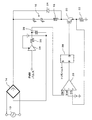
図1は、一実施形態の構成を示す図である。交流電源10は、例えば、家庭のコンセントなどから利用できる100V、50Hz(または60Hz)商用電源である。この交流電源10からの交流電力は、トライアック調光器12に供給される。トライアック調光器12は、別途供給される、供給電力についての制御信号に応じて、交流電源10からの交流電流の波形の一部を除去して、トライアックパルスを生成する。例えば、電力を50%にするとの制御信号であれば、1周期の交流波形の50%をカットする。この場合、交流波形の1周期のうち、1°〜90°、180°〜270°をカットすることで、電力を50%にする。これは、ゲート回路などによって、容易に行える。
FIG. 1 is a diagram illustrating a configuration of an embodiment. The
トライアック調光器12からのトライアックパルスは、全波整流器14に供給される。この全波整流器14は、ダイオードなどの整流素子を用い、正弦波形の負側を正側に反転させた波形に変換する。
The triac pulse from the
この全波整流器14の順方向出力端は、1以上の所定数のLEDの直列接続からなるLED列16のアノード側端に接続されている。このLED列16のカソード端には、コイル18の一端が接続され、このコイル18の他端は、制御トランジスタ20、電流検出抵抗22を介し、アースに接続されている。また、コイル18と制御トランジスタ20の接続点には、ダイオード24のアノードが接続され、このダイオード24のカソードは、LED列16と全波整流器14の順方向出力端の接続点に接続されている。
The forward output end of the full-
電流検出抵抗22と制御トランジスタ20の接続点の電圧CSが、コンパレータ26の正入力端に入力されている。このコンパレータ26の第1負入力端には、基準電圧Vrefが入力されており、コンパレータ26は、電流検出点の電圧が基準電圧Vrefを上回ったときにHレベルを出力する。
A voltage CS at a connection point between the
コンパレータ26の出力は、フリップフロップ28のリセット端に入力されている。このフリップフロップ28のセット端には、トライアックパルスに比べて十分高い周波数のトリガパルスが供給されている。そして、フリップフロップ28のQ出力が制御トランジスタ20のゲートに接続されている。従って、トリガパルスが印加されると制御トランジスタ20はオンの状態となる。
The output of the
制御トランジスタ20がオンの状態において、全波整流器14からの出力が、LED列16を介しコイル18に印加され、このコイル18を介しアースに向かって流れる電流検出端の電圧CSが基準電圧Vrefを上回った時点で、制御トランジスタ20がオフされる。そして、このときにコイル18にたまったエネルギーによってダイオード24を介し、LED列16への電流が継続される。このような動作がトライアックパルスの半周期毎に繰り返され、LED列16の発光量がトライアックパルスの導通角(デューティー)によって制御される。
When the
このような回路では、トライアック調光器12からのトライアックパルスが安定せず、例えば半周期毎のパルス電圧が異なる場合、制御トランジスタ20がオフするタイミングが半周期毎に異なり、LED列16の発光量が変化して、ちらつきが生じてしまう。
In such a circuit, when the triac pulse from the
そこで、本実施形態では、コンパレータ26に第2負入力端子を設け、ここに第2の基準電圧となる電圧SMTを入力する。この電圧SMTについて説明する。
Therefore, in the present embodiment, the
全波整流器14の出力は、分圧抵抗30,30によって所定の電圧に調整され、コンパレータ32の正入力端に入力されている。コンパレータ32の負入力端には、所定の基準電圧が入力されており、コンパレータ32は、全波整流器14の出力が所定値以上の場合にHレベルを出力する。コンパレータ32の出力は、アンプ34によって所定のDCシフトの後、抵抗36を介し、コンデンサ38に充電される。すなわち、アンプ34の出力が抵抗36を介しコンデンサ38の一端に供給され、コンデンサ38の他端は、全波整流器14の逆方向出力端に接続されている。なお、分圧抵抗の下側端も全波整流器14の逆方向出力端に接続されており、コンパレータ32の負入力端に入力される基準電圧も全波整流器14の逆方向出力端の電圧(アース電圧)を基準として形成されている。
The output of the full-
そして、抵抗36とコンデンサ38の接続端の電圧が電圧SMTとしてコンパレータ26の第2負入力端に供給されている。この電圧SMTは、分圧抵抗30,30の抵抗値、コンパレータ32の負入力端に入力される基準電圧値、アンプ34におけるDCオフセット量によって、トライアックパルスの導通角に対する電圧値が決定され、抵抗36の抵抗値およびコンデンサ38の容量値によって、時定数が変化するが、抵抗36およびコンデンサ38からなる積分回路によって、トライアックパルスがDC電圧化されるため、半周期毎電圧の変化にはよらない電圧となる。従って、毎回のLED列16の点灯を均一にすることができ、ちらつきの発生を抑制することができる。また、トライアックパルスの導通角が狭い場合には、電圧SMTも小さくなり、比較的早いタイミングで制御トランジスタ20がオフされ、適切なLED列16に対する電流供給が行える。さらに、コンパレータ26の第1負入力端には基準電圧Vrefが入力されており、電圧SMTが基準電圧Vrefより高くなった場合には、電圧CSが基準電圧Vrefを上回った時点で、制御トランジスタ20がオフされる。
The voltage at the connection end of the
なお、コンパレータ32を省略すると、オフセット量が変化するが、その場合はアンプ34におけるオフセット量を調整すればよい。
If the
図2には、他の実施形態が示されている。この構成では、分圧抵抗30,30の出力電圧は、インバータ40において反転されるとともに、オフセット量を適切に設定してから抵抗36を介しコンデンサ38に充電される。すなわち、トライアックの導通角に応じてコンデンサ38の充電電圧が変動し、それが検出電圧CSに重畳される。従って、トライアックの導通角が狭いときにCS電圧を上昇させ、導通角が広いときにCS電圧を低下させる制御が行われる。そこで、導通角が狭いときにCS電圧が高くして基準電圧Vrefにすぐ到達するようにでき、LED列16に流れる電流を絞ることができる。また、逆に導通角が広いときにCS電圧が低くして基準電圧Vrefに到達するのを遅くでき、LED列16に流れる電流を十分なものにできる。
FIG. 2 shows another embodiment. In this configuration, the output voltages of the
このように、トライアックパルスを直流電圧に変換し、この電圧をCS電圧に加えることで1回あたりのトライアックパルスのばらつきがちらつき要因にならないようにすることができる。 In this way, by converting the triac pulse into a DC voltage and adding this voltage to the CS voltage, the variation of the triac pulse per one time can be prevented from flickering.
図3は、さらに他の実施形態の構成を示している。この例では、トライアック調光器12を用いるのではなく、外部から入力されるPWM信号を用いて調光を行う。
FIG. 3 shows a configuration of still another embodiment. In this example, the
すなわち、交流電源10からの交流電力はそのまま全波整流器14に供給され、全波整流されてLED列16に印加される。また、制御トランジスタ20は、フリップフロップ28の出力によってオンオフされる。
That is, the AC power from the
このような構成において、フリップフロップ28の出力をアンドゲートに入力し、このアンドゲートにPWMパルスを入力することが考えられる。これによって、PWMパルスのLレベルの期間にフリップフロップ28の出力がオフされ、その期間制御トランジスタ20をオフして、調光することができる。
In such a configuration, it is conceivable that the output of the flip-
しかし、この場合において、PWMパルスの周波数が、交流電圧の周波数に近いぐらいまで落ちてくるとちらつきが見えてしまう。 However, in this case, flickering can be seen when the frequency of the PWM pulse drops to a level close to the frequency of the AC voltage.
本実施形態では、PWMパルスを直流電圧化して得られた電圧SMTを利用して、図1の例と同様に制御トランジスタ20のスイッチングを制御する。
In the present embodiment, the switching of the
すなわち、外部から入力されてくるPWMパルスをアンプ34に入力し、ここで所定のオフセットをして得られた出力を抵抗36を介し、コンデンサ38にする。そして、得られた直流電圧SMTをコンパレータ32の第2負入力端に入力する。この構成によっても、図1の実施形態と同様に電圧SMTを用いて制御トランジスタ20のスイッチングを制御することができる。そして、PWMパルス信号のディーティー比を調光程度に応じたデューティー比のとすることで、図1の構成とほぼ同様に動作が得られる。
That is, an externally input PWM pulse is input to the
従って、本実施形態の構成によれば、交流電圧の周波数に近いぐらいまでPWM周波数が落ちてきても、PWMパルスのデューティー比が直流電圧に変換されているために周波数が落ちてもちらつきが出ずに調光が可能となる。 Therefore, according to the configuration of the present embodiment, even if the PWM frequency drops to a level close to the frequency of the AC voltage, flickering occurs even if the frequency drops because the duty ratio of the PWM pulse is converted to a DC voltage. Dimming is possible without
図4は、さらに他の実施形態の構成を示している。この例では、図3と同様に、PWMパルスを直流電圧化して、これを検出電圧CSに重畳することで、図2の例と同様に制御トランジスタ20のスイッチングを制御する。
FIG. 4 shows a configuration of still another embodiment. In this example, as in FIG. 3, the PWM pulse is converted into a DC voltage and this is superimposed on the detection voltage CS to control the switching of the
すなわち、外部から入力されるPWMパルスをオフセット電圧を調整できるインバータ40に入力し、ここで所定のオフセットをするとともに反転して得られた出力を抵抗36を介し、コンデンサ38にする。そして、得られた検出電圧CSに重畳する。この構成によって、PWM制御の外部入力パルスのデューティー比が大きいほど、コンデンサ38に得られる充電電圧が小さくなる。そこで、図2の実施形態と同様に、外部入力パルスのデューティー比が大きいほど、コンパレータ32において出力がHレベルになるのが遅くなり、従って制御トランジスタ20のオフが遅いタイミングになるような制御が行われる。そして、外部入力信号をトライアック調光器12から出力されるトライアックの導通角に対応するディーティー比のPWM信号とすることで、図2の構成とほぼ同様に動作が得られる。
That is, an externally input PWM pulse is input to an
なお、PWMパルスがHレベルの場合にスイッチングをオフするようなものであれば、インバータ40に代えて、単なるアンプを用いればよい。
It should be noted that a simple amplifier may be used in place of the
このように、本実施形態の構成によっても、交流電圧の周波数に近いぐらいまでPWM周波数が落ちても、ちらつきが出ずに調光が可能となる。 As described above, even with the configuration of the present embodiment, even if the PWM frequency drops to a level close to the frequency of the AC voltage, dimming can be performed without flickering.
図5には、さらに他の実施形態の構成を示してある。この例では、トランス50を用いて、LED列16の駆動系と、交流電源10に接続されている系から絶縁している。すなわち、全波整流器14の順方向出力端は、トランス50の一次側コイルの一端に接続されており、このトランス50の一次側コイルの他端が制御トランジスタ20、電流検出抵抗22を介しアースに接続されている。すなわち、この経路にはLED列16が設けられていない。従って、制御トランジスタ20のオンオフによって、トランス50の一次側コイルに全波整流器14の出力に応じた周波数の交流電流が流れ、トランス50の二次側コイルには、一次側コイルに流れる電流に対応した交流電流が流れる。
FIG. 5 shows a configuration of still another embodiment. In this example, the
トランス50の二次側コイルの一端には、ダイオード24を介し、LED列16のアノードが接続され、二次側コイルの他端には、LED列16のカソードが接続されているとともに、このLED列16と並列してコンデンサ52が接続されている。
The anode of the
従って、トランス50の二次側コイルに流れる電流が整流されてダイオード24を介し、LED列16に電流が流れ、LED列16のLEDが発光する。また、LED列16に並列接続されているコンデンサ52によってLED列16に流れる電流が平滑化される。
Therefore, the current flowing through the secondary coil of the
なお、制御トランジスタ20をオンオフする構成は、図3と同様である。
The configuration for turning on and off the
このような図5の構成によって、LED列16が電源系と切り離されるため、LEDに人が触れても安全である。特に、交流電源10として、200V系が用いられる場合には、このような電源系と、LEDの駆動系を切り離すことが好適である。
With such a configuration of FIG. 5, the
また、この例では、電源系におけるトランス50の一次側コイルの電流制御系を図3の構成としたが、図1,2,4の構成にも同様に適用することができる。
In this example, the current control system of the primary coil of the
そして、このようなトランス50を用いた場合にも、制御信号を直流電圧に変換することで、LEDの発光の際のちらつきを防止することができる。
Even when such a
なお、電流検出抵抗22が電流センス回路、コンパレータ26が比較回路、コンパレータ26から、制御トランジスタ20のゲートまでの回路が制御回路に該当する。
The
10 交流電源、12 トライアック調光器、14 全波整流器、16 LED列、18 コイル、20 制御トランジスタ、22 電流検出抵抗、24 ダイオード、26,32 コンパレータ、28 フリップフロップ、30 分圧抵抗、34 アンプ、36 抵抗、38 コンデンサ、40 インバータ。
10 AC power supply, 12 Triac dimmer, 14 Full-wave rectifier, 16 LED array, 18 coil, 20 Control transistor, 22 Current detection resistor, 24 Diode, 26, 32 Comparator, 28 Flip-flop, 30 Voltage divider resistor, 34
Claims (2)
トライアック調光器からのトライアックパルスを全波整流する全波整流回路と、
全波整流回路の出力が印加されLEDに流れる駆動電流を検出する電流センス回路と、
前記駆動電流をオンオフする制御トランジスタと、
電流センス回路により検出した駆動電流値と所定値とを比較する比較回路と、
この比較回路の比較結果に応じて駆動電流値が大きいときに前記制御トランジスタをオフし、トリガパルスが印加された場合に前記制御トランジスタをオンする制御回路と、
前記トライアックパルスをDC電圧信号に変換する変換回路と、
前記DC電圧信号に応じて、前記比較回路に入力される、前記駆動電流値または前記所定値を変更する変更手段と、
を有することを特徴とするLED調光回路。 A triac dimmer that gates the AC waveform from the AC power source at a rate according to the control signal and outputs a triac pulse with a part of the waveform missing,
A full-wave rectification circuit that full-wave rectifies the triac pulse from the triac dimmer;
A current sense circuit that detects the drive current that flows through the LED when the output of the full-wave rectifier circuit is applied;
A control transistor for turning on and off the drive current;
A comparison circuit for comparing the drive current value detected by the current sense circuit with a predetermined value;
A control circuit that turns off the control transistor when a drive current value is large according to a comparison result of the comparison circuit, and turns on the control transistor when a trigger pulse is applied;
A conversion circuit for converting the triac pulse into a DC voltage signal;
Changing means for changing the drive current value or the predetermined value input to the comparison circuit according to the DC voltage signal;
An LED dimming circuit comprising:
全波整流回路の出力が印加されLEDに流れる駆動電流を検出する電流センス回路と、
前記駆動電流をオンオフする制御トランジスタと、
電流センス回路により検出した駆動電流値を所定値と比較し、駆動電流値が所定値を超えたときに前記制御トランジスタをオフし、トリガパルスが印加された場合に前記制御トランジスタをオンする制御回路と、
外部から入力されてくる調光程度を示すPWM信号をDC電圧信号に変換する変換回路と、
前記DC電圧信号に応じて、前記比較回路に入力される、前記駆動電流値または前記所定値を変更する変更手段と、
を有することを特徴とするLED調光回路。 A full-wave rectifier circuit for full-wave rectification of an AC waveform from an AC power supply
A current sense circuit that detects the drive current that flows through the LED when the output of the full-wave rectifier circuit is applied;
A control transistor for turning on and off the drive current;
A control circuit that compares a drive current value detected by a current sense circuit with a predetermined value, turns off the control transistor when the drive current value exceeds a predetermined value, and turns on the control transistor when a trigger pulse is applied When,
A conversion circuit for converting a PWM signal indicating the degree of dimming input from the outside into a DC voltage signal;
Changing means for changing the drive current value or the predetermined value input to the comparison circuit according to the DC voltage signal;
An LED dimming circuit comprising:
Priority Applications (4)
| Application Number | Priority Date | Filing Date | Title |
|---|---|---|---|
| JP2011073265A JP5780803B2 (en) | 2011-03-29 | 2011-03-29 | LED dimming circuit |
| KR1020120031818A KR20120112146A (en) | 2011-03-29 | 2012-03-28 | Led dimming circuit |
| US13/432,798 US8736194B2 (en) | 2011-03-29 | 2012-03-28 | LED dimmer circuit |
| CN201210089431.0A CN102740549B (en) | 2011-03-29 | 2012-03-29 | Led light adjusting circuit |
Applications Claiming Priority (1)
| Application Number | Priority Date | Filing Date | Title |
|---|---|---|---|
| JP2011073265A JP5780803B2 (en) | 2011-03-29 | 2011-03-29 | LED dimming circuit |
Publications (2)
| Publication Number | Publication Date |
|---|---|
| JP2012209103A true JP2012209103A (en) | 2012-10-25 |
| JP5780803B2 JP5780803B2 (en) | 2015-09-16 |
Family
ID=46926297
Family Applications (1)
| Application Number | Title | Priority Date | Filing Date |
|---|---|---|---|
| JP2011073265A Active JP5780803B2 (en) | 2011-03-29 | 2011-03-29 | LED dimming circuit |
Country Status (4)
| Country | Link |
|---|---|
| US (1) | US8736194B2 (en) |
| JP (1) | JP5780803B2 (en) |
| KR (1) | KR20120112146A (en) |
| CN (1) | CN102740549B (en) |
Families Citing this family (40)
| Publication number | Priority date | Publication date | Assignee | Title |
|---|---|---|---|---|
| US9380665B2 (en) | 2009-08-14 | 2016-06-28 | Once Innovations, Inc. | Spectral shift control for dimmable AC LED lighting |
| US8373363B2 (en) | 2009-08-14 | 2013-02-12 | Once Innovations, Inc. | Reduction of harmonic distortion for LED loads |
| US8553439B2 (en) * | 2010-02-09 | 2013-10-08 | Power Integrations, Inc. | Method and apparatus for determining zero-crossing of an AC input voltage to a power supply |
| US9482397B2 (en) | 2010-03-17 | 2016-11-01 | Once Innovations, Inc. | Light sources adapted to spectral sensitivity of diurnal avians and humans |
| US8773031B2 (en) * | 2010-11-22 | 2014-07-08 | Innosys, Inc. | Dimmable timer-based LED power supply |
| US8742695B2 (en) | 2012-05-14 | 2014-06-03 | Usai, Llc | Lighting control system and method |
| WO2013173284A1 (en) * | 2012-05-14 | 2013-11-21 | Usai, Llc | Lighting system having a dimming color simulating an incandescent light |
| US8456109B1 (en) * | 2012-05-14 | 2013-06-04 | Usai, Llc | Lighting system having a dimming color simulating an incandescent light |
| US8581520B1 (en) | 2012-05-14 | 2013-11-12 | Usai, Llc | Lighting system having a dimming color simulating an incandescent light |
| CN103209516B (en) * | 2012-12-20 | 2015-09-16 | 上海显恒光电科技股份有限公司 | LED dimming method and dimming circuit adopting same |
| US9572210B2 (en) | 2012-12-28 | 2017-02-14 | Silicon Works Co., Ltd. | Control circuit of light-emitting diode lighting apparatus |
| US9265119B2 (en) | 2013-06-17 | 2016-02-16 | Terralux, Inc. | Systems and methods for providing thermal fold-back to LED lights |
| CN103327694B (en) * | 2013-06-26 | 2015-07-22 | 上海晶丰明源半导体有限公司 | Silicon controlled dimming LED drive circuit |
| CN105474755B (en) * | 2013-07-03 | 2018-07-17 | 万斯创新公司 | For the spectral shift control of tunable optical AC LED illuminations |
| WO2015017655A1 (en) | 2013-08-02 | 2015-02-05 | Once Innovations, Inc. | System and method of illuminating livestock |
| CN103533721B (en) * | 2013-10-31 | 2015-08-26 | 矽力杰半导体技术(杭州)有限公司 | Pulse type current LED drive circuit |
| CN103561503B (en) * | 2013-11-19 | 2015-07-08 | 无锡安特源科技有限公司 | A kind of LED driving power suitable for AC phase-cut dimming |
| US9148919B2 (en) * | 2013-12-06 | 2015-09-29 | Semiconductor Components Industries, Llc | Method for mitigating flicker |
| US9247603B2 (en) | 2014-02-11 | 2016-01-26 | Once Innovations, Inc. | Shunt regulator for spectral shift controlled light source |
| KR102257718B1 (en) * | 2014-10-01 | 2021-05-28 | 매그나칩 반도체 유한회사 | Circuit driving light emitting diode and light apparatus comprising the same |
| CN105530720A (en) * | 2014-10-17 | 2016-04-27 | 昌旸科技股份有限公司 | Driving device and method thereof |
| WO2016065573A1 (en) * | 2014-10-30 | 2016-05-06 | Texas Instruments Incorporated | Led current controller |
| CN204145859U (en) * | 2014-11-14 | 2015-02-04 | 云梦云曦灯饰制品有限公司 | Lamp string |
| US9872351B2 (en) * | 2015-04-07 | 2018-01-16 | Liteideas, Llc | Device and method for encoding a signal on alternating current lines |
| US10078055B2 (en) | 2015-05-19 | 2018-09-18 | AVID Labs, LLC | LED strobe |
| TWI563872B (en) | 2015-11-05 | 2016-12-21 | Ind Tech Res Inst | Dimming control method and circuit thereof |
| EP3437437B1 (en) | 2016-03-29 | 2023-07-26 | Signify North America Corporation | System and method of illuminating livestock |
| CN105934040B (en) * | 2016-06-15 | 2018-06-19 | 陕西亚成微电子股份有限公司 | A kind of light adjusting circuit |
| US10314125B2 (en) | 2016-09-30 | 2019-06-04 | Once Innovations, Inc. | Dimmable analog AC circuit |
| US10542601B2 (en) | 2017-07-25 | 2020-01-21 | Liteideas, Llc | Smart dimming system incorporating a three-pin connector |
| TWI635776B (en) * | 2017-11-23 | 2018-09-11 | 晶豪科技股份有限公司 | Controller for switching regulator, switching regulator and led lighting system |
| CN110049596B (en) * | 2019-04-28 | 2024-02-20 | 拓尔微电子股份有限公司 | A pulse input detection circuit for white LED dimming |
| US10716187B1 (en) * | 2019-11-08 | 2020-07-14 | Gan Power Technology Co., Ltd. | LED driving structure |
| US11871490B2 (en) * | 2020-03-24 | 2024-01-09 | Rohm Co., Ltd. | Lighting control device, lighting device, and vehicle |
| CN111405733B (en) * | 2020-03-26 | 2024-09-27 | 杭州涂鸦信息技术有限公司 | Intelligent dimming and color temperature adjusting circuit |
| CN113966646B (en) * | 2020-05-21 | 2024-02-09 | 日清纺微电子有限公司 | Lighting system |
| US11277895B1 (en) * | 2021-03-25 | 2022-03-15 | Silicon Laboratories Inc. | LED driver control using MCU |
| JP7684562B2 (en) * | 2021-07-30 | 2025-05-28 | ミツミ電機株式会社 | Dimming control device and dimming device |
| CN117729660A (en) * | 2023-10-17 | 2024-03-19 | 杰华特微电子股份有限公司 | A lighting circuit and its control method |
| CN119922788B (en) * | 2025-01-23 | 2026-03-06 | 宁波赛耐比光电科技有限公司 | A dimming power supply |
Citations (3)
| Publication number | Priority date | Publication date | Assignee | Title |
|---|---|---|---|---|
| JP2002231471A (en) * | 2001-01-31 | 2002-08-16 | Toshiba Lighting & Technology Corp | LED lighting device and lighting device |
| JP2010244958A (en) * | 2009-04-09 | 2010-10-28 | Sanyo Electric Co Ltd | Light emitting element control circuit |
| JP2010287430A (en) * | 2009-06-11 | 2010-12-24 | Shihen Tech Corp | LED lighting device |
Family Cites Families (7)
| Publication number | Priority date | Publication date | Assignee | Title |
|---|---|---|---|---|
| CN1274078C (en) * | 2003-04-30 | 2006-09-06 | 徐成 | Intelligent remote-control contact light-modulating switch |
| JP2010198943A (en) | 2009-02-26 | 2010-09-09 | Eiji Kino | Led lighting system using conduction angle control-type and voltage variable-type dimmer for dimming light |
| JP2010284031A (en) * | 2009-06-05 | 2010-12-16 | Sharp Corp | Switching power supply device and lighting device using the same |
| KR20110028149A (en) * | 2009-09-11 | 2011-03-17 | 삼성엘이디 주식회사 | Lamp drive circuit reduces power consumption of switching control ICs |
| CN102143628B (en) * | 2010-01-29 | 2013-05-08 | 成都芯源系统有限公司 | Circuit and method and lamp using circuit |
| JP2011165394A (en) * | 2010-02-05 | 2011-08-25 | Sharp Corp | Led drive circuit, dimming device, led illumination fixture, led illumination device, and led illumination system |
| CN103313472B (en) * | 2010-05-19 | 2016-02-03 | 成都芯源系统有限公司 | LED drive circuit with dimming function and lamp |
-
2011
- 2011-03-29 JP JP2011073265A patent/JP5780803B2/en active Active
-
2012
- 2012-03-28 US US13/432,798 patent/US8736194B2/en active Active
- 2012-03-28 KR KR1020120031818A patent/KR20120112146A/en not_active Abandoned
- 2012-03-29 CN CN201210089431.0A patent/CN102740549B/en active Active
Patent Citations (3)
| Publication number | Priority date | Publication date | Assignee | Title |
|---|---|---|---|---|
| JP2002231471A (en) * | 2001-01-31 | 2002-08-16 | Toshiba Lighting & Technology Corp | LED lighting device and lighting device |
| JP2010244958A (en) * | 2009-04-09 | 2010-10-28 | Sanyo Electric Co Ltd | Light emitting element control circuit |
| JP2010287430A (en) * | 2009-06-11 | 2010-12-24 | Shihen Tech Corp | LED lighting device |
Also Published As
| Publication number | Publication date |
|---|---|
| US8736194B2 (en) | 2014-05-27 |
| KR20120112146A (en) | 2012-10-11 |
| CN102740549B (en) | 2015-08-26 |
| JP5780803B2 (en) | 2015-09-16 |
| US20120249000A1 (en) | 2012-10-04 |
| CN102740549A (en) | 2012-10-17 |
Similar Documents
| Publication | Publication Date | Title |
|---|---|---|
| JP5780803B2 (en) | LED dimming circuit | |
| TWI420972B (en) | Circuits for driving light source, methods for controlling dimming of light source, driving systems, and controllers for regulating brightness of light source | |
| CN102474953B (en) | Dimming device for a lighting apparatus | |
| JP5576819B2 (en) | Lighting device and lighting apparatus | |
| CN103139987B (en) | Lighting apparatus and illuminating fixture with the same | |
| US8872444B2 (en) | Lighting device for solid-state light source and illumination apparatus including same | |
| CN103139955B (en) | Apparatus for lighting and the ligthing paraphernalia with this apparatus for lighting | |
| TWI586211B (en) | Dipole lighting device with synchronous pulse width modulation dimming control | |
| CN102752907A (en) | Lighting driver circuit and light fixture | |
| JP5671016B2 (en) | Power interface with LED for TRIAC dimmer | |
| CN103974502A (en) | Electronic control device of LED light engine and application thereof | |
| EP3128815B1 (en) | Light-dimming device | |
| EP3183941A1 (en) | Ballast circuit | |
| KR20120082912A (en) | Dimmable lighting system | |
| JP2011233450A (en) | Control circuit of light-emitting element | |
| US20180235048A1 (en) | Light-dimming device | |
| JP2014517466A (en) | LED retrofit drive circuit and method for operating LED retrofit drive circuit | |
| JP2013026079A (en) | Led lighting device | |
| KR20110104337A (en) | Unidirectional LED module device with harmonic attenuation | |
| TWI593313B (en) | Dimming controller, drive circuit and control method | |
| JP5475718B2 (en) | LED lighting circuit and LED lamp provided with the same | |
| KR20110035837A (en) | Dimmer for light emitting device | |
| JP2017142969A (en) | Dimming circuit | |
| EP2926624B1 (en) | Halogen retrofit led lighting device using an electronic transformer and a controller | |
| US9356534B1 (en) | Method and apparatus for turning on a lighting device |
Legal Events
| Date | Code | Title | Description |
|---|---|---|---|
| A621 | Written request for application examination |
Free format text: JAPANESE INTERMEDIATE CODE: A621 Effective date: 20140303 |
|
| A977 | Report on retrieval |
Free format text: JAPANESE INTERMEDIATE CODE: A971007 Effective date: 20141113 |
|
| A131 | Notification of reasons for refusal |
Free format text: JAPANESE INTERMEDIATE CODE: A131 Effective date: 20141118 |
|
| A601 | Written request for extension of time |
Free format text: JAPANESE INTERMEDIATE CODE: A601 Effective date: 20150218 |
|
| A521 | Request for written amendment filed |
Free format text: JAPANESE INTERMEDIATE CODE: A523 Effective date: 20150310 |
|
| A131 | Notification of reasons for refusal |
Free format text: JAPANESE INTERMEDIATE CODE: A131 Effective date: 20150407 |
|
| A521 | Request for written amendment filed |
Free format text: JAPANESE INTERMEDIATE CODE: A523 Effective date: 20150622 |
|
| TRDD | Decision of grant or rejection written | ||
| A01 | Written decision to grant a patent or to grant a registration (utility model) |
Free format text: JAPANESE INTERMEDIATE CODE: A01 Effective date: 20150707 |
|
| A61 | First payment of annual fees (during grant procedure) |
Free format text: JAPANESE INTERMEDIATE CODE: A61 Effective date: 20150714 |
|
| R150 | Certificate of patent or registration of utility model |
Ref document number: 5780803 Country of ref document: JP Free format text: JAPANESE INTERMEDIATE CODE: R150 |
|
| R250 | Receipt of annual fees |
Free format text: JAPANESE INTERMEDIATE CODE: R250 |
|
| R250 | Receipt of annual fees |
Free format text: JAPANESE INTERMEDIATE CODE: R250 |
|
| R250 | Receipt of annual fees |
Free format text: JAPANESE INTERMEDIATE CODE: R250 |
|
| R250 | Receipt of annual fees |
Free format text: JAPANESE INTERMEDIATE CODE: R250 |
|
| R250 | Receipt of annual fees |
Free format text: JAPANESE INTERMEDIATE CODE: R250 |
|
| R250 | Receipt of annual fees |
Free format text: JAPANESE INTERMEDIATE CODE: R250 |
|
| R250 | Receipt of annual fees |
Free format text: JAPANESE INTERMEDIATE CODE: R250 |
|
| R250 | Receipt of annual fees |
Free format text: JAPANESE INTERMEDIATE CODE: R250 |