JP2012209805A - 信号処理基板及び局回線終端装置 - Google Patents
信号処理基板及び局回線終端装置 Download PDFInfo
- Publication number
- JP2012209805A JP2012209805A JP2011074601A JP2011074601A JP2012209805A JP 2012209805 A JP2012209805 A JP 2012209805A JP 2011074601 A JP2011074601 A JP 2011074601A JP 2011074601 A JP2011074601 A JP 2011074601A JP 2012209805 A JP2012209805 A JP 2012209805A
- Authority
- JP
- Japan
- Prior art keywords
- signal processing
- board
- processing board
- printed wiring
- housing
- Prior art date
- Legal status (The legal status is an assumption and is not a legal conclusion. Google has not performed a legal analysis and makes no representation as to the accuracy of the status listed.)
- Granted
Links
Images


Landscapes
- Mounting Of Printed Circuit Boards And The Like (AREA)
- Structure Of Telephone Exchanges (AREA)
- Engineering & Computer Science (AREA)
- Computer Networks & Wireless Communication (AREA)
- Microelectronics & Electronic Packaging (AREA)
Abstract
【解決手段】信号処理基板4は、OLT1に収容される信号処理基板であって、印刷配線基板11と、印刷配線基板11に通信ケーブル8を接続するためのケーブルコネクタ7と、を備え、信号処理基板4は、OLT1の筐体2の開口面から挿抜され、ケーブルコネクタ7は、印刷配線基板11の外周に沿った複数の辺21〜24のうち、信号処理基板4を筐体2内に収容した際に開口面に露出する辺21とは異なる辺23に配置されている。
【選択図】図6
Description
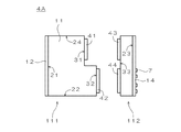
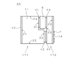
図7及び図8は、第1の変形例に係る信号処理基板4Aの構成を模式的に示す側面図である。信号処理基板4Aの印刷配線基板11は、前面側の印刷配線基板111(第1基板)と、背面側の印刷配線基板112(第2基板)とに分かれている。図7には印刷配線基板111,112が分離された状態を示しており、図8には印刷配線基板111,112が接続された状態を示している。信号処理基板4Aを構成する複数の回路をどのように印刷配線基板111,112に振り分けるかは任意であるが、例えば、電源回路を印刷配線基板112に振り分け、その他の回路を印刷配線基板111に振り分けることができる。
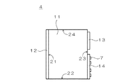
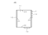
図9は、第2の変形例に係る信号処理基板4Bの構成を模式的に示す側面図である。印刷配線基板11の前面側の辺21には全長に亘って表示板12が固定されており、背面側の辺23には全長に亘ってコネクタ取付板14が固定されており、底面側の辺22(第3の辺)には電源コネクタ13が固定されている。本変形例において、電源基板6は筐体2の底面に固定されており、印刷配線基板11は電源コネクタ13を介して電源基板6に接続される。
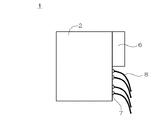
本実施の形態に係る信号処理基板4によれば、図6に示したように、ケーブルコネクタ7は、印刷配線基板11の外周に沿った複数の辺21〜24のうち、信号処理基板4を筐体2内に収容した際に前面の第1の開口面に露出する辺21とは異なる辺23に配置されている。信号処理基板4はOLT1の筐体2の第1の開口面から挿抜されるため、第1の開口面に露出する辺21とは異なる辺23にケーブルコネクタ7を配置することにより、信号処理基板4を挿抜する側の面に通信ケーブル8は存在しない。その結果、保守等のために信号処理基板4を筐体2から抜き出す際に通信ケーブル8が作業の障害となる事態を回避できるため、作業性を向上することが可能となる。
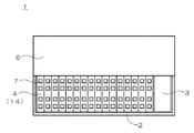
2 筐体
4,4A,4B 信号処理基板
6 電源基板
7 ケーブルコネクタ
8 通信ケーブル
11,111,112 印刷配線基板
13,41,43 電源コネクタ
14 コネクタ取付板
21〜24 辺
42,44 コネクタ
Claims (7)
- 局回線終端装置に収容される信号処理基板であって、
印刷配線基板と、
前記印刷配線基板に通信ケーブルを接続するためのケーブルコネクタと、
を備え、
前記信号処理基板は、前記局回線終端装置の筐体の開口面から挿抜され、
前記ケーブルコネクタは、前記印刷配線基板の外周に沿った複数の辺のうち、前記信号処理基板を前記筐体内に収容した際に前記開口面に露出する第1の辺とは異なる第2の辺に配置されている、信号処理基板。 - 前記信号処理基板は、
前記第1の辺を含む第1基板と、
前記第2の辺を含む第2基板と、
を有しており、
前記第1基板及び前記第2基板は、両基板間の基板接続部において、互いに接続及び分離が可能である、請求項1に記載の信号処理基板。 - 前記基板接続部は、
前記第1基板及び前記第2基板に電源を供給する電源基板と、
前記第1基板及び前記第2基板間で信号を送受するための信号接続部と、
を有する、請求項2に記載の信号処理基板。 - 前記信号処理基板に電源を供給する電源基板を接続するための電源コネクタをさらに備え、
前記電源コネクタは前記第2の辺に配置されている、請求項1に記載の信号処理基板。 - 前記信号処理基板に電源を供給する電源基板を接続するための電源コネクタをさらに備え、
前記電源コネクタは、前記印刷配線基板の外周に沿った複数の辺のうち、前記第1の辺及び前記第2の辺とは異なる第3の辺に配置されている、請求項1に記載の信号処理基板。 - 前記筐体内には複数の前記信号処理基板が並んで収容され、
各前記信号処理基板の前記第2の辺には、隣り合う前記信号処理基板同士の隙間を塞ぐ金属板が固定されており、
前記ケーブルコネクタは、前記金属板に取り付けられている、請求項1〜5のいずれか一つに記載の信号処理基板。 - 筐体と、
前記筐体内に収容される信号処理基板と、
を備え、
前記信号処理基板は、
印刷配線基板と、
前記印刷配線基板に通信ケーブルを接続するためのケーブルコネクタと、
を有し、
前記信号処理基板は、前記筐体の第1の開口面から挿抜され、
前記ケーブルコネクタは、前記印刷配線基板の外周に沿った複数の辺のうち、前記信号処理基板を前記筐体内に収容した際に前記第1の開口面に露出する第1の辺とは異なる第2の辺に配置されており、
前記ケーブルコネクタは、前記筐体の第2の開口面に露出する、局回線終端装置。
Priority Applications (1)
| Application Number | Priority Date | Filing Date | Title |
|---|---|---|---|
| JP2011074601A JP5617101B2 (ja) | 2011-03-30 | 2011-03-30 | 信号処理基板及び局回線終端装置 |
Applications Claiming Priority (1)
| Application Number | Priority Date | Filing Date | Title |
|---|---|---|---|
| JP2011074601A JP5617101B2 (ja) | 2011-03-30 | 2011-03-30 | 信号処理基板及び局回線終端装置 |
Publications (2)
| Publication Number | Publication Date |
|---|---|
| JP2012209805A true JP2012209805A (ja) | 2012-10-25 |
| JP5617101B2 JP5617101B2 (ja) | 2014-11-05 |
Family
ID=47189192
Family Applications (1)
| Application Number | Title | Priority Date | Filing Date |
|---|---|---|---|
| JP2011074601A Active JP5617101B2 (ja) | 2011-03-30 | 2011-03-30 | 信号処理基板及び局回線終端装置 |
Country Status (1)
| Country | Link |
|---|---|
| JP (1) | JP5617101B2 (ja) |
Citations (14)
| Publication number | Priority date | Publication date | Assignee | Title |
|---|---|---|---|---|
| JPS56155600A (en) * | 1980-04-30 | 1981-12-01 | Fujitsu Ltd | Method of detecting erroneous insertion of printed board |
| JPS6135596A (ja) * | 1984-07-27 | 1986-02-20 | 富士通株式会社 | コネクタ接続構造 |
| JPS62126697A (ja) * | 1985-11-27 | 1987-06-08 | 三菱電機株式会社 | 基板格納装置 |
| JPH0282692A (ja) * | 1988-09-20 | 1990-03-23 | Toshiba Corp | 電子機器 |
| JPH0458593A (ja) * | 1990-06-28 | 1992-02-25 | Fujitsu Ltd | 電子装置のシェルフの構造 |
| JPH0555781A (ja) * | 1991-08-26 | 1993-03-05 | Fujitsu Ltd | 電子装置のシールド構造 |
| JPH0637890A (ja) * | 1992-07-15 | 1994-02-10 | Nec Corp | 回線種別照合方式 |
| JP2000059825A (ja) * | 1998-08-03 | 2000-02-25 | Nippon Telegr & Teleph Corp <Ntt> | 通信サービスシステムにおける光加入者線終端装置箱及びそれに用いる電磁波遮蔽装置 |
| JP2000147269A (ja) * | 1998-09-01 | 2000-05-26 | Fujitsu Ltd | 電子装置 |
| JP2002353663A (ja) * | 2001-05-22 | 2002-12-06 | Fujitsu Ltd | 通信装置 |
| JP2003224376A (ja) * | 2002-01-30 | 2003-08-08 | Sumitomo Electric Ind Ltd | 集線装置及び整束具 |
| JP2004029701A (ja) * | 2002-04-30 | 2004-01-29 | Sumitomo Electric Ind Ltd | 集線装置及び光ファイバ余長処理方法 |
| JP2005116751A (ja) * | 2003-10-07 | 2005-04-28 | Fujitsu Ltd | プラグインユニット、筺体及び電子装置 |
| WO2008146517A1 (ja) * | 2007-05-29 | 2008-12-04 | The Furukawa Electric Co., Ltd. | 加入者宅側光回線終端装置及び光伝送システム |
-
2011
- 2011-03-30 JP JP2011074601A patent/JP5617101B2/ja active Active
Patent Citations (14)
| Publication number | Priority date | Publication date | Assignee | Title |
|---|---|---|---|---|
| JPS56155600A (en) * | 1980-04-30 | 1981-12-01 | Fujitsu Ltd | Method of detecting erroneous insertion of printed board |
| JPS6135596A (ja) * | 1984-07-27 | 1986-02-20 | 富士通株式会社 | コネクタ接続構造 |
| JPS62126697A (ja) * | 1985-11-27 | 1987-06-08 | 三菱電機株式会社 | 基板格納装置 |
| JPH0282692A (ja) * | 1988-09-20 | 1990-03-23 | Toshiba Corp | 電子機器 |
| JPH0458593A (ja) * | 1990-06-28 | 1992-02-25 | Fujitsu Ltd | 電子装置のシェルフの構造 |
| JPH0555781A (ja) * | 1991-08-26 | 1993-03-05 | Fujitsu Ltd | 電子装置のシールド構造 |
| JPH0637890A (ja) * | 1992-07-15 | 1994-02-10 | Nec Corp | 回線種別照合方式 |
| JP2000059825A (ja) * | 1998-08-03 | 2000-02-25 | Nippon Telegr & Teleph Corp <Ntt> | 通信サービスシステムにおける光加入者線終端装置箱及びそれに用いる電磁波遮蔽装置 |
| JP2000147269A (ja) * | 1998-09-01 | 2000-05-26 | Fujitsu Ltd | 電子装置 |
| JP2002353663A (ja) * | 2001-05-22 | 2002-12-06 | Fujitsu Ltd | 通信装置 |
| JP2003224376A (ja) * | 2002-01-30 | 2003-08-08 | Sumitomo Electric Ind Ltd | 集線装置及び整束具 |
| JP2004029701A (ja) * | 2002-04-30 | 2004-01-29 | Sumitomo Electric Ind Ltd | 集線装置及び光ファイバ余長処理方法 |
| JP2005116751A (ja) * | 2003-10-07 | 2005-04-28 | Fujitsu Ltd | プラグインユニット、筺体及び電子装置 |
| WO2008146517A1 (ja) * | 2007-05-29 | 2008-12-04 | The Furukawa Electric Co., Ltd. | 加入者宅側光回線終端装置及び光伝送システム |
Also Published As
| Publication number | Publication date |
|---|---|
| JP5617101B2 (ja) | 2014-11-05 |
Similar Documents
| Publication | Publication Date | Title |
|---|---|---|
| US9196999B2 (en) | Two-part modular connector and smart managed interconnect link using the two-part modular connector | |
| US8686870B2 (en) | Physical layer management for interconnect configurations using RFID chip technology | |
| US8678674B2 (en) | Optical transceiver and production method thereof | |
| US20050074990A1 (en) | Optics pack | |
| EP3396971B1 (en) | Physical layer management | |
| US9007206B2 (en) | Patch panel and intelligent structured cabling system | |
| US9864154B1 (en) | Field replaceable modular optical interconnect unit with optical module for datacenter switch system | |
| CN102754452A (zh) | 具有外部光连接器的光背板机架组件 | |
| RU2690032C2 (ru) | Конструкция и реализации системы для коробки с шиной данных ("data bus-in-a-box") | |
| US20110293225A1 (en) | Photoelectric conversion module and photoelectric conversion device | |
| EP3521882B1 (en) | Line card and optical network device | |
| US9459426B2 (en) | Optical plenum | |
| KR102837909B1 (ko) | 광전자 모듈, 광전자 플러그 커넥터 및 광전자 하위 배전 유닛 | |
| JP5617101B2 (ja) | 信号処理基板及び局回線終端装置 | |
| CN114079211B (zh) | 通信设备 | |
| JP2705853B2 (ja) | ラックに挿入可能な装置用の光信号接続装置 | |
| US9215814B2 (en) | Electronics assembly divider plate | |
| EP2892179B1 (en) | Connecting apparatus and system | |
| CN102143404A (zh) | 智能型结构的布缆系统与连接口 | |
| US9952399B2 (en) | Connector panel for plug-in units of a telecommunication system and associated shelf | |
| CN109347692A (zh) | 一种网速测试装置 | |
| JP2005079874A (ja) | メディアコンバータ | |
| JP2016225467A (ja) | 通信モジュール及び伝送装置 | |
| KR100581055B1 (ko) | 통신용 단자반 조립구조 | |
| EP2083486A1 (en) | Electromagnetic shielding of a connector arrangement |
Legal Events
| Date | Code | Title | Description |
|---|---|---|---|
| A625 | Written request for application examination (by other person) |
Free format text: JAPANESE INTERMEDIATE CODE: A625 Effective date: 20131023 |
|
| A977 | Report on retrieval |
Free format text: JAPANESE INTERMEDIATE CODE: A971007 Effective date: 20140528 |
|
| A131 | Notification of reasons for refusal |
Free format text: JAPANESE INTERMEDIATE CODE: A131 Effective date: 20140604 |
|
| A521 | Request for written amendment filed |
Free format text: JAPANESE INTERMEDIATE CODE: A523 Effective date: 20140725 |
|
| TRDD | Decision of grant or rejection written | ||
| A01 | Written decision to grant a patent or to grant a registration (utility model) |
Free format text: JAPANESE INTERMEDIATE CODE: A01 Effective date: 20140819 |
|
| A61 | First payment of annual fees (during grant procedure) |
Free format text: JAPANESE INTERMEDIATE CODE: A61 Effective date: 20140825 |
|
| R150 | Certificate of patent or registration of utility model |
Ref document number: 5617101 Country of ref document: JP Free format text: JAPANESE INTERMEDIATE CODE: R150 |
|
| S531 | Written request for registration of change of domicile |
Free format text: JAPANESE INTERMEDIATE CODE: R313531 |
|
| R350 | Written notification of registration of transfer |
Free format text: JAPANESE INTERMEDIATE CODE: R350 |
|
| S111 | Request for change of ownership or part of ownership |
Free format text: JAPANESE INTERMEDIATE CODE: R313113 |
|
| R371 | Transfer withdrawn |
Free format text: JAPANESE INTERMEDIATE CODE: R371 |
|
| S111 | Request for change of ownership or part of ownership |
Free format text: JAPANESE INTERMEDIATE CODE: R313113 |
|
| R350 | Written notification of registration of transfer |
Free format text: JAPANESE INTERMEDIATE CODE: R350 |
|
| R250 | Receipt of annual fees |
Free format text: JAPANESE INTERMEDIATE CODE: R250 |
|
| R250 | Receipt of annual fees |
Free format text: JAPANESE INTERMEDIATE CODE: R250 |
|
| R250 | Receipt of annual fees |
Free format text: JAPANESE INTERMEDIATE CODE: R250 |
|
| R250 | Receipt of annual fees |
Free format text: JAPANESE INTERMEDIATE CODE: R250 |
|
| R250 | Receipt of annual fees |
Free format text: JAPANESE INTERMEDIATE CODE: R250 |
|
| R250 | Receipt of annual fees |
Free format text: JAPANESE INTERMEDIATE CODE: R250 |
|
| R250 | Receipt of annual fees |
Free format text: JAPANESE INTERMEDIATE CODE: R250 |
|
| R250 | Receipt of annual fees |
Free format text: JAPANESE INTERMEDIATE CODE: R250 |
|
| R250 | Receipt of annual fees |
Free format text: JAPANESE INTERMEDIATE CODE: R250 |