JP2012242843A - 液晶表示パネル及びその駆動方法 - Google Patents
液晶表示パネル及びその駆動方法 Download PDFInfo
- Publication number
- JP2012242843A JP2012242843A JP2012117384A JP2012117384A JP2012242843A JP 2012242843 A JP2012242843 A JP 2012242843A JP 2012117384 A JP2012117384 A JP 2012117384A JP 2012117384 A JP2012117384 A JP 2012117384A JP 2012242843 A JP2012242843 A JP 2012242843A
- Authority
- JP
- Japan
- Prior art keywords
- liquid crystal
- wiring
- crystal display
- display panel
- reflective
- Prior art date
- Legal status (The legal status is an assumption and is not a legal conclusion. Google has not performed a legal analysis and makes no representation as to the accuracy of the status listed.)
- Granted
Links
Images



Classifications
-
- G—PHYSICS
- G02—OPTICS
- G02F—OPTICAL DEVICES OR ARRANGEMENTS FOR THE CONTROL OF LIGHT BY MODIFICATION OF THE OPTICAL PROPERTIES OF THE MEDIA OF THE ELEMENTS INVOLVED THEREIN; NON-LINEAR OPTICS; FREQUENCY-CHANGING OF LIGHT; OPTICAL LOGIC ELEMENTS; OPTICAL ANALOGUE/DIGITAL CONVERTERS
- G02F1/00—Devices or arrangements for the control of the intensity, colour, phase, polarisation or direction of light arriving from an independent light source, e.g. switching, gating or modulating; Non-linear optics
- G02F1/01—Devices or arrangements for the control of the intensity, colour, phase, polarisation or direction of light arriving from an independent light source, e.g. switching, gating or modulating; Non-linear optics for the control of the intensity, phase, polarisation or colour
- G02F1/13—Devices or arrangements for the control of the intensity, colour, phase, polarisation or direction of light arriving from an independent light source, e.g. switching, gating or modulating; Non-linear optics for the control of the intensity, phase, polarisation or colour based on liquid crystals, e.g. single liquid crystal display cells
- G02F1/133—Constructional arrangements; Operation of liquid crystal cells; Circuit arrangements
- G02F1/1333—Constructional arrangements; Manufacturing methods
- G02F1/13338—Input devices, e.g. touch panels
-
- G—PHYSICS
- G06—COMPUTING OR CALCULATING; COUNTING
- G06F—ELECTRIC DIGITAL DATA PROCESSING
- G06F3/00—Input arrangements for transferring data to be processed into a form capable of being handled by the computer; Output arrangements for transferring data from processing unit to output unit, e.g. interface arrangements
- G06F3/01—Input arrangements or combined input and output arrangements for interaction between user and computer
- G06F3/03—Arrangements for converting the position or the displacement of a member into a coded form
- G06F3/041—Digitisers, e.g. for touch screens or touch pads, characterised by the transducing means
- G06F3/0412—Digitisers structurally integrated in a display
-
- G—PHYSICS
- G06—COMPUTING OR CALCULATING; COUNTING
- G06F—ELECTRIC DIGITAL DATA PROCESSING
- G06F3/00—Input arrangements for transferring data to be processed into a form capable of being handled by the computer; Output arrangements for transferring data from processing unit to output unit, e.g. interface arrangements
- G06F3/01—Input arrangements or combined input and output arrangements for interaction between user and computer
- G06F3/03—Arrangements for converting the position or the displacement of a member into a coded form
- G06F3/041—Digitisers, e.g. for touch screens or touch pads, characterised by the transducing means
- G06F3/0414—Digitisers, e.g. for touch screens or touch pads, characterised by the transducing means using force sensing means to determine a position
- G06F3/04146—Digitisers, e.g. for touch screens or touch pads, characterised by the transducing means using force sensing means to determine a position using pressure sensitive conductive elements delivering a boolean signal and located between crossing sensing lines, e.g. located between X and Y sensing line layers
-
- G—PHYSICS
- G09—EDUCATION; CRYPTOGRAPHY; DISPLAY; ADVERTISING; SEALS
- G09G—ARRANGEMENTS OR CIRCUITS FOR CONTROL OF INDICATING DEVICES USING STATIC MEANS TO PRESENT VARIABLE INFORMATION
- G09G3/00—Control arrangements or circuits, of interest only in connection with visual indicators other than cathode-ray tubes
- G09G3/20—Control arrangements or circuits, of interest only in connection with visual indicators other than cathode-ray tubes for presentation of an assembly of a number of characters, e.g. a page, by composing the assembly by combination of individual elements arranged in a matrix no fixed position being assigned to or needed to be assigned to the individual characters or partial characters
- G09G3/34—Control arrangements or circuits, of interest only in connection with visual indicators other than cathode-ray tubes for presentation of an assembly of a number of characters, e.g. a page, by composing the assembly by combination of individual elements arranged in a matrix no fixed position being assigned to or needed to be assigned to the individual characters or partial characters by control of light from an independent source
- G09G3/36—Control arrangements or circuits, of interest only in connection with visual indicators other than cathode-ray tubes for presentation of an assembly of a number of characters, e.g. a page, by composing the assembly by combination of individual elements arranged in a matrix no fixed position being assigned to or needed to be assigned to the individual characters or partial characters by control of light from an independent source using liquid crystals
-
- G—PHYSICS
- G02—OPTICS
- G02F—OPTICAL DEVICES OR ARRANGEMENTS FOR THE CONTROL OF LIGHT BY MODIFICATION OF THE OPTICAL PROPERTIES OF THE MEDIA OF THE ELEMENTS INVOLVED THEREIN; NON-LINEAR OPTICS; FREQUENCY-CHANGING OF LIGHT; OPTICAL LOGIC ELEMENTS; OPTICAL ANALOGUE/DIGITAL CONVERTERS
- G02F1/00—Devices or arrangements for the control of the intensity, colour, phase, polarisation or direction of light arriving from an independent light source, e.g. switching, gating or modulating; Non-linear optics
- G02F1/01—Devices or arrangements for the control of the intensity, colour, phase, polarisation or direction of light arriving from an independent light source, e.g. switching, gating or modulating; Non-linear optics for the control of the intensity, phase, polarisation or colour
- G02F1/13—Devices or arrangements for the control of the intensity, colour, phase, polarisation or direction of light arriving from an independent light source, e.g. switching, gating or modulating; Non-linear optics for the control of the intensity, phase, polarisation or colour based on liquid crystals, e.g. single liquid crystal display cells
- G02F1/133—Constructional arrangements; Operation of liquid crystal cells; Circuit arrangements
- G02F1/136—Liquid crystal cells structurally associated with a semi-conducting layer or substrate, e.g. cells forming part of an integrated circuit
- G02F1/1362—Active matrix addressed cells
- G02F1/136286—Wiring, e.g. gate line, drain line
-
- G—PHYSICS
- G02—OPTICS
- G02F—OPTICAL DEVICES OR ARRANGEMENTS FOR THE CONTROL OF LIGHT BY MODIFICATION OF THE OPTICAL PROPERTIES OF THE MEDIA OF THE ELEMENTS INVOLVED THEREIN; NON-LINEAR OPTICS; FREQUENCY-CHANGING OF LIGHT; OPTICAL LOGIC ELEMENTS; OPTICAL ANALOGUE/DIGITAL CONVERTERS
- G02F2202/00—Materials and properties
- G02F2202/10—Materials and properties semiconductor
Landscapes
- Engineering & Computer Science (AREA)
- Physics & Mathematics (AREA)
- Theoretical Computer Science (AREA)
- General Engineering & Computer Science (AREA)
- General Physics & Mathematics (AREA)
- Nonlinear Science (AREA)
- Human Computer Interaction (AREA)
- Chemical & Material Sciences (AREA)
- Crystallography & Structural Chemistry (AREA)
- Mathematical Physics (AREA)
- Optics & Photonics (AREA)
- Liquid Crystal (AREA)
- Computer Hardware Design (AREA)
- Devices For Indicating Variable Information By Combining Individual Elements (AREA)
Abstract
【解決手段】本発明の液晶表示パネルは、アレイ基板と、カラーフィルター基板、及び、両基板間の液晶層と、を備え、前記アレイ基板上にゲートライン、データライン、及び、ゲートラインとデータラインにより限定した画素ユニットが形成され、前記カラーフィルター基板の内側に内蔵タッチ装置が設けられ、当該内蔵タッチ装置は、第1の配線と第2の配線とを備え、前記第1の配線と前記第2の配線は2層構造であり、且つ、両配線が重なり合っている領域に前記第1の配線と前記第2の配線との間に位置する半導体層が設けられる。
【選択図】図1
Description
(1)液晶表示パネルの内蔵タッチ装置の第2の配線42に第2電圧を印加し、前記内蔵タッチ装置の第1の配線41に第1電圧を印加し、且つ、第1電圧と第2電圧は等しくなく、非タッチ状態で、第1の配線41と第2の配線42との間の半導体層43の導通電流はデータ処理ユニットの識別電流より小さい。
例えば、前記第2電圧は0より大きく、且つ共通電圧より大きくない。第1電圧は第2電圧より大きくてもよいし、第2電圧より小さくてもよい。例えば、第1電圧が第2電圧より小さい場合の効果はよりよい。実際の応用において、実際の需要に応じて第1配線と第2の配線との間に適当な電圧差があればよい。
101:第1電圧を前記内蔵タッチ装置の第1の配線41に印加するとともに、第2電圧を液晶表示パネルの内蔵タッチ装置の第2の配線42に印加し、第1電圧と第2電圧とは等しくなく、
非タッチ状態で、第1の配線41と第2の配線42との間の半導体層43の導通電流はデータ処理ユニットの識別電流より小さく、
好ましくは、前記第2電圧は0より大きく、且つ共通電圧より大きくない。第1電圧は第2電圧より大きくてもよいし、第2電圧より小さくてもよい。例えば、第1電圧が第2電圧より小さい場合の効果はよりよい。実際の応用において、実際の需要に応じて第1配線と第2の配線との間に適当な電圧差を有するようにしてよい。
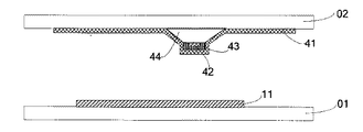
タッチ状態で、タッチ位置の内蔵タッチ装置の半導体層43は、圧力の作用でアレイ基板のゲートライン11に近づく。該ゲートライン11のオン電圧は該タッチ装置の半導体層43の導通電流を増大させる。この場合に、第1の配線41と第2の配線42は半導体層43の電流信号をデータ処理ユニットに伝達し、データ処理ユニットは比較を介してこの場合の導通電流が該データ処理ユニットの識別電流より小さくないことを得て、データ処理ユニットは第1の配線41と第2の配線42の電流信号の変化によって該タッチ位置を確定する。
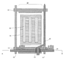
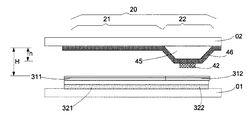
02−カラーフィルター基板のベース基板
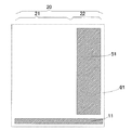
11−ゲートライン
12−データライン
20−画素ユニット
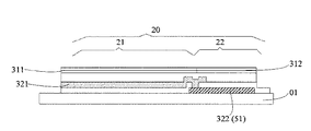
21−透過表示領域
22−反射表示領域
31−共通電極
32−画素電極
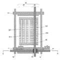
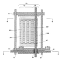
311−透過表示領域の共通電極
312−反射表示領域の共通電極
321−透過表示領域の画素電極
322−反射表示領域の画素電極
41−第1の配線
42−第2の配線
43−半導体層
44−支持物
45−有機層
46−カラーフィルター層
51−反射層
Claims (18)
- 液晶表示パネルであって、
アレイ基板と、
カラーフィルター基板と、
両基板間に挟まれる液晶層と、を備え、
前記アレイ基板上にゲートラインとデータラインが形成され、ゲートラインとデータラインにより画素ユニットが限定され、前記カラーフィルター基板の内側に内蔵タッチ装置が設けられ、該内蔵タッチ装置は、
第1の配線と第2の配線とを備え、前記第1の配線と前記第2の配線は2層構造であり、且つ両配線が重なり合っている領域に前記第1の配線と前記第2の配線との間に位置する半導体層が設けられることを特徴とする液晶表示パネル。 - 各前記画素ユニットは透過表示領域と反射表示領域とを備え、
前記第1の配線は前記カラーフィルター基板上に形成され、且つ前記アレイ基板上の少なくとも1本のゲートラインに対向して設置され、前記第2の配線は前記カラーフィルター基板上に形成され、且つ前記アレイ基板上の少なくとも1列の画素ユニットの反射表示領域に対向して設置され、又は、前記アレイ基板上の少なくとも1本のデータラインに対向して設置されることを特徴とする請求項1に記載の液晶表示パネル。 - 前記画素ユニットの反射表示領域に反射層が形成され、且つ該反射層は前記ゲートライン又は前記データラインと同層であることを特徴とする請求項2に記載の液晶表示パネル。
- 前記反射表示領域において、前記カラーフィルター基板のベース基板とカラーフィルター層との間に有機層が形成され、該有機層は反射表示領域と透過表示領域の光電曲線を一致させることを特徴とする請求項2又は3に記載の液晶表示パネル。
- 前記反射表示領域の有機層の厚さは前記透過表示領域の液晶層の厚さの半分であることを特徴とする請求項4に記載の液晶表示パネル。
- 前記画素ユニットの反射表示領域に反射層が形成され、且つ該反射層は前記ゲートラインと同層であるとともに、ビアホールを介して前記画素ユニットの透過表示領域の画素電極に接続されることを特徴とする請求項2に記載の液晶表示パネル。
- 前記画素ユニットにおける、反射表示領域の共通電極の形状と、透過表示領域の共通電極との形状が異なることにより、該画素ユニットの反射表示領域と透過表示領域との光電曲線を一致させることを特徴とする請求項2又は3に記載の液晶表示パネル。
- 前記透過表示領域の共通電極の形状はストリップ状であり、前記反射表示領域の共通電極の形状は透過表示領域の共通電極の形状と平行しないストリップ状であることを特徴とする請求項7に記載の液晶表示パネル。
- 前記透過表示領域のストリップ状の共通電極と前記反射領域のストリップ状の共通電極との夾角は45度であることを特徴とする請求項8に記載の液晶表示パネル。
- 前記画素ユニットにおける、反射表示領域の画素電極の形状と、透過表示領域の画素電極との形状とが異なることにより、該画素ユニットにおける反射表示領域と透過表示領域との光電曲線を一致させることを特徴とする請求項2又は3に記載の液晶表示パネル。
- 前記透過表示領域の画素電極の形状はストリップ状であり、前記反射表示領域の画素電極の形状は透過表示領域の画素電極の形状と平行しないストリップ状であることを特徴とする請求項10に記載の液晶表示パネル。
- 前記透過表示領域のストリップ状の画素電極と前記反射領域のストリップ状の画素電極との夾角は45度であることを特徴とする請求項11に記載の液晶表示パネル。
- 前記第1の配線は前記カラーフィルター基板上に形成され、且つ前記アレイ基板上の少なくとも1本のゲートラインに対向して設置され、前記第2の配線は前記カラーフィルター基板上に形成され、且つ前記アレイ基板上の少なくとも1本のデータラインに対向して設置されることを特徴とする請求項1に記載の液晶表示パネル。
- 前記両配線が重なり合っている領域に設けられた前記第1の配線と前記第2の配線との間に位置される半導体層は、非結晶シリコン又は多結晶シリコンより製作された半導体層であることを特徴とする請求項1〜13のいずれか一項に記載の液晶表示パネル。
- 前記カラーフィルター基板における第1の配線と第2の配線との重なり合っている領域は、前記アレイ基板におけるゲートラインとデータラインとの重なり合っている領域に対向しないことを特徴とする請求項1〜13のいずれか一項に記載の液晶表示パネル。
- 前記内蔵タッチ装置と前記カラーフィルター基板との間に支持物が形成され、該支持物は前記両配線が重なり合っている領域に位置されることを特徴とする請求項1〜13のいずれか一項に記載の液晶表示パネル。
- 請求項1ないし16のいずれか一項に記載の液晶表示パネルを駆動する方法であって、
第1電圧を前記内蔵タッチ装置の第1の配線に印加するとともに、第2電圧を液晶表示パネルの内蔵タッチ装置の第2の配線に印加するが、第1電圧と第2電圧とが等しくなく、
非タッチ状態で、第1の配線と第2の配線との間における半導体層の導通電流はデータ処理ユニットの識別電流より小さく、
タッチ状態で、タッチ位置の半導体層の導通電流はゲートラインのオン電圧の作用で前記データ処理ユニットの識別電流より小さくなく、前記第1の配線と第2の配線は半導体層の電流信号をデータ処理ユニットに伝達することより、前記データ処理ユニットは電流信号の変化によってタッチ位置に対して確定することを特徴とする液晶表示パネルの駆動方法。 - 前記第2電圧は0より大きく、且つ共通電圧より大きくないことを特徴とする請求項17に記載の液晶表示パネルの駆動方法。
Applications Claiming Priority (2)
| Application Number | Priority Date | Filing Date | Title |
|---|---|---|---|
| CN201110134525.0 | 2011-05-23 | ||
| CN201110134525 | 2011-05-23 |
Publications (2)
| Publication Number | Publication Date |
|---|---|
| JP2012242843A true JP2012242843A (ja) | 2012-12-10 |
| JP6054634B2 JP6054634B2 (ja) | 2016-12-27 |
Family
ID=46545227
Family Applications (1)
| Application Number | Title | Priority Date | Filing Date |
|---|---|---|---|
| JP2012117384A Active JP6054634B2 (ja) | 2011-05-23 | 2012-05-23 | 液晶表示パネル及びその駆動方法 |
Country Status (5)
| Country | Link |
|---|---|
| US (1) | US8947384B2 (ja) |
| EP (1) | EP2527912B1 (ja) |
| JP (1) | JP6054634B2 (ja) |
| KR (1) | KR101452279B1 (ja) |
| CN (1) | CN102629052B (ja) |
Families Citing this family (12)
| Publication number | Priority date | Publication date | Assignee | Title |
|---|---|---|---|---|
| CN102929031B (zh) * | 2012-10-31 | 2015-06-10 | 北京京东方光电科技有限公司 | 彩膜基板及其制造方法、触摸显示装置及其驱动方法 |
| CN102999220B (zh) * | 2012-11-30 | 2015-07-22 | 北京京东方光电科技有限公司 | 一种半透半反式内嵌触摸屏、其驱动方法及显示装置 |
| CN103137558B (zh) * | 2013-02-06 | 2016-10-05 | 京东方科技集团股份有限公司 | 一种tn型阵列基板及其制作方法、显示装置 |
| CN103970353B (zh) * | 2014-04-29 | 2016-10-05 | 京东方科技集团股份有限公司 | 一种触控显示面板及触控显示装置 |
| CN105319782A (zh) * | 2014-07-30 | 2016-02-10 | 群创光电股份有限公司 | 显示面板与显示装置 |
| JP6417953B2 (ja) * | 2015-01-15 | 2018-11-07 | オムロン株式会社 | 表示装置 |
| CN106128374A (zh) * | 2015-05-06 | 2016-11-16 | 义隆电子股份有限公司 | 非分时触控及显示的内嵌式液晶显示器及其驱动方法 |
| TWI591524B (zh) * | 2015-06-05 | 2017-07-11 | 群創光電股份有限公司 | 顯示裝置 |
| JP6146594B1 (ja) * | 2015-12-22 | 2017-06-14 | カシオ計算機株式会社 | 表示装置及びその制御方法、制御プログラム |
| CN106293298B (zh) * | 2016-08-15 | 2018-11-20 | 京东方科技集团股份有限公司 | 触控显示基板及其制备方法、触控显示装置 |
| CN108428723B (zh) * | 2018-03-27 | 2021-08-03 | 京东方科技集团股份有限公司 | 像素界定结构及其制备方法、显示基板、喷墨打印方法 |
| KR102859194B1 (ko) * | 2021-12-28 | 2025-09-11 | 엘지디스플레이 주식회사 | 액정표시장치 |
Citations (7)
| Publication number | Priority date | Publication date | Assignee | Title |
|---|---|---|---|---|
| JPS63216382A (ja) * | 1987-03-05 | 1988-09-08 | Ishida Scales Mfg Co Ltd | 荷重センサ |
| JP2006040289A (ja) * | 2004-07-26 | 2006-02-09 | Samsung Electronics Co Ltd | 感知素子を内蔵した液晶表示装置 |
| JP2006226769A (ja) * | 2005-02-16 | 2006-08-31 | Hitachi Metals Ltd | 圧力センサ用複合セラミックス材料およびこれを用いた圧力センサ |
| JP2007047734A (ja) * | 2005-07-15 | 2007-02-22 | Sanyo Epson Imaging Devices Corp | 液晶装置及び電子機器 |
| JP2007183583A (ja) * | 2005-12-05 | 2007-07-19 | Semiconductor Energy Lab Co Ltd | 液晶表示装置 |
| WO2008108042A1 (ja) * | 2007-03-01 | 2008-09-12 | Sharp Kabushiki Kaisha | 表示パネル用基板、表示パネル、表示装置、および表示パネル用基板の製造方法 |
| JP2009217098A (ja) * | 2008-03-12 | 2009-09-24 | Seiko Epson Corp | 液晶装置 |
Family Cites Families (11)
| Publication number | Priority date | Publication date | Assignee | Title |
|---|---|---|---|---|
| DE10340188A1 (de) * | 2003-09-01 | 2005-04-07 | Siemens Ag | Bildschirm mit einer berührungsempfindlichen Bedienoberfläche zur Befehlseingabe |
| FR2918747A1 (fr) * | 2007-07-12 | 2009-01-16 | St Microelectronics Sa | Microcapteur de pression |
| US7924350B2 (en) * | 2007-10-12 | 2011-04-12 | Au Optronics Corporation | Capacitance type touch panel |
| US8179482B2 (en) * | 2008-03-19 | 2012-05-15 | Samsung Electronics Co., Ltd. | Touch panel display and method of manufacturing the same |
| JP5148685B2 (ja) * | 2008-03-21 | 2013-02-20 | シャープ株式会社 | タッチセンサー内蔵液晶表示装置 |
| JP5161305B2 (ja) * | 2008-06-05 | 2013-03-13 | 北陸電気工業株式会社 | タッチパネルを備えた表示装置及び圧電アクチュエータ |
| KR101009672B1 (ko) | 2008-09-12 | 2011-01-19 | 엘지디스플레이 주식회사 | 터치 패널 내장형 액정 표시 장치 |
| CN101825787B (zh) | 2009-03-04 | 2013-06-12 | 北京京东方光电科技有限公司 | 触摸显示屏及其制造方法 |
| WO2010137215A1 (ja) * | 2009-05-27 | 2010-12-02 | シャープ株式会社 | 表示装置 |
| KR101592010B1 (ko) | 2009-07-17 | 2016-02-05 | 삼성디스플레이 주식회사 | 표시 장치 및 그 제조 방법 |
| CN202177761U (zh) * | 2011-05-23 | 2012-03-28 | 北京京东方光电科技有限公司 | 一种液晶显示面板及液晶显示器件 |
-
2011
- 2011-08-12 CN CN201110231599.6A patent/CN102629052B/zh active Active
-
2012
- 2012-05-22 US US13/477,773 patent/US8947384B2/en active Active
- 2012-05-23 KR KR1020120054784A patent/KR101452279B1/ko active Active
- 2012-05-23 JP JP2012117384A patent/JP6054634B2/ja active Active
- 2012-05-23 EP EP12169048.1A patent/EP2527912B1/en active Active
Patent Citations (7)
| Publication number | Priority date | Publication date | Assignee | Title |
|---|---|---|---|---|
| JPS63216382A (ja) * | 1987-03-05 | 1988-09-08 | Ishida Scales Mfg Co Ltd | 荷重センサ |
| JP2006040289A (ja) * | 2004-07-26 | 2006-02-09 | Samsung Electronics Co Ltd | 感知素子を内蔵した液晶表示装置 |
| JP2006226769A (ja) * | 2005-02-16 | 2006-08-31 | Hitachi Metals Ltd | 圧力センサ用複合セラミックス材料およびこれを用いた圧力センサ |
| JP2007047734A (ja) * | 2005-07-15 | 2007-02-22 | Sanyo Epson Imaging Devices Corp | 液晶装置及び電子機器 |
| JP2007183583A (ja) * | 2005-12-05 | 2007-07-19 | Semiconductor Energy Lab Co Ltd | 液晶表示装置 |
| WO2008108042A1 (ja) * | 2007-03-01 | 2008-09-12 | Sharp Kabushiki Kaisha | 表示パネル用基板、表示パネル、表示装置、および表示パネル用基板の製造方法 |
| JP2009217098A (ja) * | 2008-03-12 | 2009-09-24 | Seiko Epson Corp | 液晶装置 |
Also Published As
| Publication number | Publication date |
|---|---|
| KR101452279B1 (ko) | 2014-10-22 |
| JP6054634B2 (ja) | 2016-12-27 |
| CN102629052B (zh) | 2014-08-06 |
| EP2527912A1 (en) | 2012-11-28 |
| US8947384B2 (en) | 2015-02-03 |
| CN102629052A (zh) | 2012-08-08 |
| EP2527912B1 (en) | 2015-08-26 |
| KR20120130736A (ko) | 2012-12-03 |
| US20120299901A1 (en) | 2012-11-29 |
Similar Documents
| Publication | Publication Date | Title |
|---|---|---|
| JP6054634B2 (ja) | 液晶表示パネル及びその駆動方法 | |
| US9715303B2 (en) | In-cell self capacitive touch control display panel and manufacture method thereof | |
| US8345207B2 (en) | Thin film transistor array substrate and liquid crystal display device | |
| CN101236319B (zh) | 带输入功能的显示装置 | |
| CN102436323B (zh) | 嵌有触摸面板的显示设备及其制造方法 | |
| KR101749146B1 (ko) | 터치 스크린이 내장된 액정 표시장치와 이의 제조방법 | |
| CN100412631C (zh) | 液晶装置及电子设备 | |
| CN102566181B (zh) | 显示面板 | |
| CN102629606B (zh) | 阵列基板及其制备方法和显示装置 | |
| US20130314371A1 (en) | In-Cell Touch Display Panel Structure with Metal Layer for Sensing | |
| TWI690755B (zh) | 畫素結構 | |
| US9207483B2 (en) | In-cell touch display panel structure with metal layer on lower substrate for sensing | |
| CN102193229A (zh) | 触摸感测式液晶显示装置及其制造方法 | |
| CN106062619A (zh) | 液晶显示装置 | |
| WO2016201762A1 (zh) | IPS型On Cell触控显示面板及其制作方法 | |
| US9857620B2 (en) | Display device | |
| CN101750780A (zh) | 液晶面板和液晶显示器件 | |
| US10955710B2 (en) | Display panels and electronic devices | |
| US20180196545A1 (en) | Cell touch screen, method for driving the same, and display device | |
| CN103346160B (zh) | 阵列基板及其制作方法、显示装置 | |
| CN102629047B (zh) | 像素单元、阵列基板、液晶面板及显示设备 | |
| WO2017000333A1 (zh) | IPS型In Cell触控显示面板及其制作方法 | |
| CN105470266B (zh) | Ffs型阵列基板及其制作方法 | |
| CN107562280A (zh) | 压力触控显示装置及制作和驱动方法 | |
| TWI403809B (zh) | 邊緣電場切換模式液晶顯示器及其製造方法 |
Legal Events
| Date | Code | Title | Description |
|---|---|---|---|
| A621 | Written request for application examination |
Free format text: JAPANESE INTERMEDIATE CODE: A621 Effective date: 20150424 |
|
| A977 | Report on retrieval |
Free format text: JAPANESE INTERMEDIATE CODE: A971007 Effective date: 20151021 |
|
| A131 | Notification of reasons for refusal |
Free format text: JAPANESE INTERMEDIATE CODE: A131 Effective date: 20151130 |
|
| A521 | Request for written amendment filed |
Free format text: JAPANESE INTERMEDIATE CODE: A523 Effective date: 20160226 |
|
| A131 | Notification of reasons for refusal |
Free format text: JAPANESE INTERMEDIATE CODE: A131 Effective date: 20160715 |
|
| A521 | Request for written amendment filed |
Free format text: JAPANESE INTERMEDIATE CODE: A523 Effective date: 20161017 |
|
| TRDD | Decision of grant or rejection written | ||
| A01 | Written decision to grant a patent or to grant a registration (utility model) |
Free format text: JAPANESE INTERMEDIATE CODE: A01 Effective date: 20161107 |
|
| A61 | First payment of annual fees (during grant procedure) |
Free format text: JAPANESE INTERMEDIATE CODE: A61 Effective date: 20161201 |
|
| R150 | Certificate of patent or registration of utility model |
Ref document number: 6054634 Country of ref document: JP Free format text: JAPANESE INTERMEDIATE CODE: R150 |
|
| R250 | Receipt of annual fees |
Free format text: JAPANESE INTERMEDIATE CODE: R250 |
|
| R250 | Receipt of annual fees |
Free format text: JAPANESE INTERMEDIATE CODE: R250 |
|
| R250 | Receipt of annual fees |
Free format text: JAPANESE INTERMEDIATE CODE: R250 |
|
| R250 | Receipt of annual fees |
Free format text: JAPANESE INTERMEDIATE CODE: R250 |
|
| R250 | Receipt of annual fees |
Free format text: JAPANESE INTERMEDIATE CODE: R250 |
|
| R250 | Receipt of annual fees |
Free format text: JAPANESE INTERMEDIATE CODE: R250 |
|
| R250 | Receipt of annual fees |
Free format text: JAPANESE INTERMEDIATE CODE: R250 |