JP2012247705A - Polarization conversion element, polarization conversion unit, and projection type video device - Google Patents
Polarization conversion element, polarization conversion unit, and projection type video device Download PDFInfo
- Publication number
- JP2012247705A JP2012247705A JP2011120966A JP2011120966A JP2012247705A JP 2012247705 A JP2012247705 A JP 2012247705A JP 2011120966 A JP2011120966 A JP 2011120966A JP 2011120966 A JP2011120966 A JP 2011120966A JP 2012247705 A JP2012247705 A JP 2012247705A
- Authority
- JP
- Japan
- Prior art keywords
- polarization conversion
- light
- translucent substrate
- crystal material
- polarization
- Prior art date
- Legal status (The legal status is an assumption and is not a legal conclusion. Google has not performed a legal analysis and makes no representation as to the accuracy of the status listed.)
- Withdrawn
Links
- 230000010287 polarization Effects 0.000 title claims abstract description 245
- 238000006243 chemical reaction Methods 0.000 title claims abstract description 141
- 239000013078 crystal Substances 0.000 claims abstract description 167
- 230000003287 optical effect Effects 0.000 claims abstract description 148
- 239000000463 material Substances 0.000 claims abstract description 147
- 239000000758 substrate Substances 0.000 claims abstract description 144
- 238000000926 separation method Methods 0.000 claims abstract description 83
- 238000005520 cutting process Methods 0.000 claims abstract description 67
- 238000013461 design Methods 0.000 claims abstract description 66
- VYPSYNLAJGMNEJ-UHFFFAOYSA-N silicon dioxide Inorganic materials O=[Si]=O VYPSYNLAJGMNEJ-UHFFFAOYSA-N 0.000 claims abstract description 59
- 239000010453 quartz Substances 0.000 claims abstract description 54
- 230000014509 gene expression Effects 0.000 claims description 40
- 239000004973 liquid crystal related substance Substances 0.000 claims description 25
- 239000002178 crystalline material Substances 0.000 claims description 14
- 238000010030 laminating Methods 0.000 claims description 6
- 235000012239 silicon dioxide Nutrition 0.000 description 54
- 239000010408 film Substances 0.000 description 45
- 230000005540 biological transmission Effects 0.000 description 29
- 239000011521 glass Substances 0.000 description 23
- 230000000694 effects Effects 0.000 description 21
- 239000010410 layer Substances 0.000 description 9
- 238000000034 method Methods 0.000 description 7
- 230000017525 heat dissipation Effects 0.000 description 6
- 238000004088 simulation Methods 0.000 description 6
- 239000000853 adhesive Substances 0.000 description 5
- 230000001070 adhesive effect Effects 0.000 description 5
- 229910052751 metal Inorganic materials 0.000 description 5
- 239000002184 metal Substances 0.000 description 5
- 238000006116 polymerization reaction Methods 0.000 description 5
- 230000008859 change Effects 0.000 description 4
- 229910010272 inorganic material Inorganic materials 0.000 description 4
- 239000011147 inorganic material Substances 0.000 description 4
- 229920003002 synthetic resin Polymers 0.000 description 4
- 239000000057 synthetic resin Substances 0.000 description 4
- 229910004298 SiO 2 Inorganic materials 0.000 description 3
- 239000012790 adhesive layer Substances 0.000 description 3
- 238000000151 deposition Methods 0.000 description 3
- 238000010586 diagram Methods 0.000 description 3
- 238000005286 illumination Methods 0.000 description 3
- 229910052594 sapphire Inorganic materials 0.000 description 3
- 239000010980 sapphire Substances 0.000 description 3
- 229910010413 TiO 2 Inorganic materials 0.000 description 2
- GWEVSGVZZGPLCZ-UHFFFAOYSA-N Titan oxide Chemical compound O=[Ti]=O GWEVSGVZZGPLCZ-UHFFFAOYSA-N 0.000 description 2
- 238000003491 array Methods 0.000 description 2
- 238000001816 cooling Methods 0.000 description 2
- 230000007423 decrease Effects 0.000 description 2
- 230000006866 deterioration Effects 0.000 description 2
- KPUWHANPEXNPJT-UHFFFAOYSA-N disiloxane Chemical class [SiH3]O[SiH3] KPUWHANPEXNPJT-UHFFFAOYSA-N 0.000 description 2
- 238000004519 manufacturing process Methods 0.000 description 2
- 230000004048 modification Effects 0.000 description 2
- 238000012986 modification Methods 0.000 description 2
- 229920000515 polycarbonate Polymers 0.000 description 2
- 239000004417 polycarbonate Substances 0.000 description 2
- 239000000377 silicon dioxide Substances 0.000 description 2
- OGIDPMRJRNCKJF-UHFFFAOYSA-N titanium oxide Inorganic materials [Ti]=O OGIDPMRJRNCKJF-UHFFFAOYSA-N 0.000 description 2
- 229910018072 Al 2 O 3 Inorganic materials 0.000 description 1
- 229910021532 Calcite Inorganic materials 0.000 description 1
- 229910001111 Fine metal Inorganic materials 0.000 description 1
- 239000004372 Polyvinyl alcohol Substances 0.000 description 1
- 235000005811 Viola adunca Nutrition 0.000 description 1
- 240000009038 Viola odorata Species 0.000 description 1
- 235000013487 Viola odorata Nutrition 0.000 description 1
- 235000002254 Viola papilionacea Nutrition 0.000 description 1
- 229910052782 aluminium Inorganic materials 0.000 description 1
- XAGFODPZIPBFFR-UHFFFAOYSA-N aluminium Chemical compound [Al] XAGFODPZIPBFFR-UHFFFAOYSA-N 0.000 description 1
- PNEYBMLMFCGWSK-UHFFFAOYSA-N aluminium oxide Inorganic materials [O-2].[O-2].[O-2].[Al+3].[Al+3] PNEYBMLMFCGWSK-UHFFFAOYSA-N 0.000 description 1
- 230000015572 biosynthetic process Effects 0.000 description 1
- 239000004020 conductor Substances 0.000 description 1
- 238000002425 crystallisation Methods 0.000 description 1
- 230000008025 crystallization Effects 0.000 description 1
- 230000002950 deficient Effects 0.000 description 1
- 238000003795 desorption Methods 0.000 description 1
- 239000000428 dust Substances 0.000 description 1
- 239000013013 elastic material Substances 0.000 description 1
- 238000001704 evaporation Methods 0.000 description 1
- 238000001746 injection moulding Methods 0.000 description 1
- 238000005304 joining Methods 0.000 description 1
- 230000007935 neutral effect Effects 0.000 description 1
- 239000012788 optical film Substances 0.000 description 1
- 125000000962 organic group Chemical group 0.000 description 1
- 239000011368 organic material Substances 0.000 description 1
- 229920006289 polycarbonate film Polymers 0.000 description 1
- -1 polyethylene terephthalate Polymers 0.000 description 1
- 229920000139 polyethylene terephthalate Polymers 0.000 description 1
- 239000005020 polyethylene terephthalate Substances 0.000 description 1
- 229920002451 polyvinyl alcohol Polymers 0.000 description 1
- 230000008569 process Effects 0.000 description 1
- 238000012545 processing Methods 0.000 description 1
- 230000001902 propagating effect Effects 0.000 description 1
- 229920005989 resin Polymers 0.000 description 1
- 239000011347 resin Substances 0.000 description 1
- 238000012552 review Methods 0.000 description 1
- 238000007493 shaping process Methods 0.000 description 1
- 229910052814 silicon oxide Inorganic materials 0.000 description 1
- 230000002194 synthesizing effect Effects 0.000 description 1
- 239000010409 thin film Substances 0.000 description 1
- 238000007740 vapor deposition Methods 0.000 description 1
Images








Classifications
-
- G—PHYSICS
- G02—OPTICS
- G02B—OPTICAL ELEMENTS, SYSTEMS OR APPARATUS
- G02B5/00—Optical elements other than lenses
- G02B5/30—Polarising elements
- G02B5/3025—Polarisers, i.e. arrangements capable of producing a definite output polarisation state from an unpolarised input state
- G02B5/3058—Polarisers, i.e. arrangements capable of producing a definite output polarisation state from an unpolarised input state comprising electrically conductive elements, e.g. wire grids, conductive particles
-
- G—PHYSICS
- G02—OPTICS
- G02B—OPTICAL ELEMENTS, SYSTEMS OR APPARATUS
- G02B27/00—Optical systems or apparatus not provided for by any of the groups G02B1/00 - G02B26/00, G02B30/00
- G02B27/28—Optical systems or apparatus not provided for by any of the groups G02B1/00 - G02B26/00, G02B30/00 for polarising
- G02B27/283—Optical systems or apparatus not provided for by any of the groups G02B1/00 - G02B26/00, G02B30/00 for polarising used for beam splitting or combining
- G02B27/285—Optical systems or apparatus not provided for by any of the groups G02B1/00 - G02B26/00, G02B30/00 for polarising used for beam splitting or combining comprising arrays of elements, e.g. microprisms
-
- G—PHYSICS
- G03—PHOTOGRAPHY; CINEMATOGRAPHY; ANALOGOUS TECHNIQUES USING WAVES OTHER THAN OPTICAL WAVES; ELECTROGRAPHY; HOLOGRAPHY
- G03B—APPARATUS OR ARRANGEMENTS FOR TAKING PHOTOGRAPHS OR FOR PROJECTING OR VIEWING THEM; APPARATUS OR ARRANGEMENTS EMPLOYING ANALOGOUS TECHNIQUES USING WAVES OTHER THAN OPTICAL WAVES; ACCESSORIES THEREFOR
- G03B21/00—Projectors or projection-type viewers; Accessories therefor
- G03B21/14—Details
- G03B21/20—Lamp housings
- G03B21/2073—Polarisers in the lamp house
-
- H—ELECTRICITY
- H04—ELECTRIC COMMUNICATION TECHNIQUE
- H04N—PICTORIAL COMMUNICATION, e.g. TELEVISION
- H04N9/00—Details of colour television systems
- H04N9/12—Picture reproducers
- H04N9/31—Projection devices for colour picture display, e.g. using electronic spatial light modulators [ESLM]
- H04N9/3141—Constructional details thereof
- H04N9/315—Modulator illumination systems
- H04N9/3167—Modulator illumination systems for polarizing the light beam
Landscapes
- Physics & Mathematics (AREA)
- General Physics & Mathematics (AREA)
- Optics & Photonics (AREA)
- Engineering & Computer Science (AREA)
- Multimedia (AREA)
- Signal Processing (AREA)
- Polarising Elements (AREA)
- Projection Apparatus (AREA)
- Liquid Crystal (AREA)
Abstract
【課題】水晶等の複屈折性と旋光性を有する結晶材料において、切断角度が設計値からずれて切断されてしまった場合でも、角度ズレに応じて、板厚を調整し、最適な設計板厚に修正することにより、設計位相差を見直し、所定の波長帯域における偏光変換効率を確実に規定値以上にする偏光変換素子の提供。
【解決手段】複屈折性と旋光性を有する結晶材料からなる透光性基板21Aと、この透光性基板21Aの入射側表面に設けられP偏光を透過させ、かつ、S偏光を反射する偏光分離部21Bとを備えて偏光分離素子21を構成し、偏光分離部21Bで反射されたS偏光Sを反射する反射素子22を、透光性基板21Aと略平行に離間して配置し、偏光分離部21Bを透過し透光性基板21Aに入射したP偏光Pを、S偏光Sの偏波面と平行となるように変換しS偏光Sとして出射するように、所定の関数を設定した。
【選択図】図1In a crystal material having birefringence and optical rotation such as quartz, even when the cutting angle is cut from the design value, the plate thickness is adjusted in accordance with the angle deviation, and the optimum design plate Providing a polarization conversion element that revises the design phase difference and ensures that the polarization conversion efficiency in a predetermined wavelength band exceeds a specified value by correcting the thickness.
A translucent substrate 21A made of a crystal material having birefringence and optical rotation, and polarized light that is provided on an incident side surface of the translucent substrate 21A and transmits P-polarized light and reflects S-polarized light. The polarization separation element 21 is configured by including the separation unit 21B, and the reflection element 22 that reflects the S-polarized light S reflected by the polarization separation unit 21B is arranged substantially in parallel with the translucent substrate 21A and is polarized. A predetermined function was set so that the P-polarized light P transmitted through the separation unit 21B and incident on the translucent substrate 21A was converted to be parallel to the polarization plane of the S-polarized light S and emitted as S-polarized light S.
[Selection] Figure 1
Description
本発明は、偏光変換素子、この偏光変換素子を備えた偏光変換ユニット及び投写型映像装置に関する。 The present invention relates to a polarization conversion element, a polarization conversion unit including the polarization conversion element, and a projection video apparatus.
液晶プロジェクター等の投影型映像装置は、光源装置から射出された光を画像情報に応じて変調し、この変調された光学像をスクリーンの上に拡大投射するものである。この液晶プロジェクターでは、光の利用効率を向上させるため、光源装置から出射されたランダムな偏光(互いに偏光面が直交するP偏光とS偏光や偏光面の方向がさまざまな直線偏光、円偏光、楕円偏光、等の偏光が混在した光)を有する光(以下、ランダム光と称す)を複数の中間光束に分割し、この分割された中間光束を1種類の直線偏光光に変換し統一して出射するために偏光変換素子が用いられている。 A projection type video apparatus such as a liquid crystal projector modulates light emitted from a light source device according to image information, and enlarges and projects the modulated optical image on a screen. In this liquid crystal projector, in order to improve the light utilization efficiency, random polarized light emitted from the light source device (P-polarized light and S-polarized light whose polarization planes are orthogonal to each other, and linearly polarized light, circularly polarized light, elliptical light with various polarization directions) The light (hereinafter, referred to as random light) having a mixed light (polarized light, etc.) is divided into a plurality of intermediate light beams, and the divided intermediate light beams are converted into one type of linearly polarized light to be output in a unified manner. For this purpose, a polarization conversion element is used.
偏光変換素子は、偏光分離膜と反射膜とを透明部材の内部に交互に配置して偏光ビームスプリッターアレイを成形し、この偏光ビームスプリッターアレイの表面に位相差板を設けた構造である。位相差板は、透明部材の光射出面側で偏光分離膜に対応した位置に所定間隔毎に複数配置されている(特許文献1)。
従来、位相差板としては、有機系材料、例えばポリカーボネートフィルム製の1/2波長板が用いられることがあり、この1/2波長板と偏光ビームスプリッターアレイとは有機系接着剤により接着されている。
この偏光変換素子の製造方法としては、両主面に偏光分離膜と反射膜とがそれぞれ形成された無色透明なガラス等の第1の透光性基板と、両主面に何も形成されていない第2の透光性基板とを交互に幾重にも積層して、或いは一方の面に偏光分離膜が形成された第1の透光性基板と、一方の面に反射膜が形成された第2の透光性基板とを交互に幾重にも積層して積層体を作り、積層面に平行な面に対して、例えば45degの角度で切断して得られた偏光ビームスプリッターアレイの光の出射面に1/2波長板が接着剤により貼り付けられている。
このように製造された偏光変換素子は、平面矩形状のフレームに組み込まれた状態で、液晶プロジェクターの光学エンジン内に搭載されている(特許文献2)。
The polarization conversion element has a structure in which a polarization beam splitter array is formed by alternately arranging polarization separation films and reflection films inside a transparent member, and a phase difference plate is provided on the surface of the polarization beam splitter array. A plurality of retardation plates are arranged at predetermined intervals on the light exit surface side of the transparent member at predetermined intervals (Patent Document 1).
Conventionally, an organic material, for example, a half-wave plate made of a polycarbonate film, may be used as the retardation plate, and the half-wave plate and the polarizing beam splitter array are bonded with an organic adhesive. Yes.
As a manufacturing method of this polarization conversion element, a first transparent substrate such as colorless and transparent glass having a polarization separation film and a reflection film formed on both main surfaces, and nothing is formed on both main surfaces. The second light-transmitting substrate that is not laminated alternately or repeatedly, or the first light-transmitting substrate having the polarization separation film formed on one surface and the reflection film formed on one surface The second light-transmitting substrate is alternately stacked several times to form a stacked body, and the polarization beam splitter array light obtained by cutting the surface parallel to the stacked surface at an angle of, for example, 45 deg. A half-wave plate is attached to the emission surface with an adhesive.
The polarization conversion element manufactured as described above is mounted in an optical engine of a liquid crystal projector in a state of being incorporated in a plane rectangular frame (Patent Document 2).
白色の光源ランプの高出力化、短アーク長化が進行し、偏光ビームスプリッターアレイ及び当該偏光ビームスプリッターアレイに接着されている1/2波長板に対する熱負荷も増大してきており、1/2波長板を構成する材料として水晶を用いて構成することが考えられている。ここで、1/2波長板を偏光ビームスプリッターアレイの光の出射面に接着させて配置する場合に用いる場合において、接着剤として、耐熱・耐光性能に優れた紫外線硬化性樹脂又は無機系材料の接着剤を用い、冷却ファンによる強制空冷を不要とする液晶プロジェクターがある(特許文献3)。 As the output of white light source lamps has been increased and the arc length has been shortened, the thermal load on the polarizing beam splitter array and the half-wave plate bonded to the polarizing beam splitter array has also increased. It is considered to use quartz as a material for the plate. Here, in the case where the half-wave plate is used while being adhered to the light exit surface of the polarizing beam splitter array, an ultraviolet curable resin or an inorganic material having excellent heat resistance and light resistance is used as an adhesive. There is a liquid crystal projector that uses an adhesive and does not require forced air cooling by a cooling fan (Patent Document 3).
さらに、平行な2面を有する透光性板材、反射膜、平行な2面を有する透光性板材、1/2波長板及び偏光分離膜がこの順序に繰り返し積層された積層体が、その積層面に対し所定の角度で切断されることで偏光分離膜と位相差板と反射膜とが切断面に対して同一の方向に傾斜した状態で配置され、互いに平行な光入射面と光出射面とを形成する偏光変換素子がある(特許文献4)。そして、特許文献4と同様構造の偏光変換素子において、1/2波長板として、切断角度がYカット(基板の主面の法線と結晶光学軸とのなす角度が90deg)で厚みが22.7〜37.1μmの水晶板を傾斜して配置したものがある(特許文献5)。さらに、1/2波長板として、板厚が21.2μm〜50.0μm,13.5μm〜31.9μmに設定し、光学軸の第1,第2光学軸方位角が16.3deg,59.6degとなる状態で、第1,第2水晶板を積層して構成された2枚の波長板が提案されている(特許文献6)。この特許文献6の従来例では、三色波長帯(波長が400nm〜700nm)での平均の偏光変換効率(三色偏光変換効率と称す)を0.8以上にすることができる。
Furthermore, a laminated body in which a translucent plate material having two parallel surfaces, a reflective film, a translucent plate material having two parallel surfaces, a half-wave plate, and a polarization separation film are repeatedly laminated in this order is By being cut at a predetermined angle with respect to the surface, the polarization separation film, the phase difference plate, and the reflection film are disposed in the same direction with respect to the cut surface, and the light incident surface and the light output surface are parallel to each other. (Patent Literature 4). In the polarization conversion element having the same structure as that of
近年、光学部品としての長寿命化の要求が増してきたことに伴って、接着剤の劣化の問題が生じてきた。
この問題を解決するために、ガラスや水晶等の2枚の透光性基板を接合する手段として、表面にシロキサン(Si−O)結合を含み、結晶化度が45%以下であるSi骨格と、該Si骨格に結合する有機基からなる脱離基とを含む接合膜とプラズマ重合法により成膜し、当該接合膜にエネルギーを付与することにより前記接合膜の表面付近に存在する前記脱離基が前記Si骨格から脱離することにより、接合膜の表面の前記領域に発現した接着性によって、前記2枚の透光性基板を接合する接合方法が提案されている(特許文献7)。
この接合方法を採用することにより、接合手段は無機化され、接合膜の劣化の問題が解決されるとともに当該接合方法を用いて接合される光学部品の長寿命化を図ることが可能となる。
そして、従来、光入射面と、この光入射面にほぼ平行な光出射面とを有し、これらの光入射面と光出射面とに沿って複数の透光性部材、偏光分離膜、反射膜、位相板及びプラズマ重合膜が配置され、複数の透光性部材のうち一部の透光性部材の傾斜面には偏光分離膜と反射膜とのいずれか一つが設けられ、透光性部材の傾斜面の表面、偏光分離膜の表面及び反射膜の表面の少なくともいずれか一つの面にプラズマ重合膜が設けられた偏光変換素子が提案されている(特許文献8)。この特許文献8の従来例では、プラズマ重合膜により、隣接する透光性部材と反射膜との間、隣接する透光性部材と位相板との間、隣接する位相板と偏光分離膜との間の少なくともいずれかが分子接合されており、プラズマ重合膜は、その主材料がポリオルガノシロキサンとされている。
In recent years, with the demand for longer life as an optical component, the problem of adhesive deterioration has arisen.
In order to solve this problem, as a means for joining two light-transmitting substrates such as glass and quartz, a Si skeleton containing a siloxane (Si—O) bond on the surface and having a crystallinity of 45% or less The desorption existing in the vicinity of the surface of the bonding film is formed by a plasma polymerization method and a bonding film including a leaving group composed of an organic group bonded to the Si skeleton, and applying energy to the bonding film There has been proposed a bonding method in which the two light-transmitting substrates are bonded to each other by the adhesiveness developed in the region on the surface of the bonding film when the group is detached from the Si skeleton (Patent Document 7).
By adopting this bonding method, the bonding means is mineralized, the problem of deterioration of the bonding film is solved, and it is possible to extend the life of optical components bonded using the bonding method.
And conventionally, it has a light incident surface and a light emitting surface substantially parallel to the light incident surface, and a plurality of translucent members, polarization separation films, and reflections along these light incident surface and light emitting surface. A film, a phase plate, and a plasma polymerized film are arranged, and one of the polarized light separation film and the reflective film is provided on the inclined surface of some of the light transmissive members among the plurality of light transmissive members. There has been proposed a polarization conversion element in which a plasma polymerization film is provided on at least one of a surface of an inclined surface of a member, a surface of a polarization separation film, and a surface of a reflection film (Patent Document 8). In the conventional example of this Patent Document 8, the plasma polymerization film is used between the adjacent translucent member and the reflective film, between the adjacent translucent member and the phase plate, and between the adjacent phase plate and the polarization separation film. At least one of them is molecularly bonded, and the main material of the plasma polymerized film is polyorganosiloxane.
しかしながら、特許文献8の従来例では、プラズマ重合膜による接合膜の膜厚は数十nmという極めて薄い膜で構成されており、この接合膜を透光性基板の表面にプラズマ重合法を用いて形成する過程で透光性基板の表面に塵やゴミ等の付着物が付着してしまうと、接合膜の膜厚よりも付着物の高さの方が遥かに高いため、付着物が付着している領域を中心として所定の領域において透光性基板同士を接合することができず、気泡などがその領域に混入してしまい、光学特性上や接合信頼性、製品寿命に大きな悪影響を与えるという課題がある。
そこで、プラズマ重合膜を用いない従来例として、特許文献9のものがある。この特許文献9では、光学ブロックは、基板上に刻設されている溝に対して板状のPBS(偏光分離素子)、ミラー及び1/2波長板、等の光学部品が装着されて構成されている。PBSはガラス板に例えばTiO2(高屈折率材料)とSiO2(低屈折率材料)とを交互に繰り返し積層してなる誘電体多層膜、等を表面蒸着することによって形成され、光の入射方向に対して所定の角度で前記基板に圧入装着されている。ミラーは長方形のガラス板に、例えば、アルミや誘電体多層膜等を表面蒸着することによって入射した光を反射することができるようになっている。そして、PBSで反射したS波を出射側に反射する角度で前記基板に装着されている。1/2波長板は、長方形のガラス板に例えばポリカーボネート、ポリビニールアルコール、ポリエチレンテレフタレートフィルムを一軸延伸した1/2位相差フィルムを貼り付けて形成されている。そして、ミラーで反射されたS波(S偏光)が入射する位置に装着され、P波(P偏光)に変換して出射する。このように、PBS、ミラー、1/2波長板等によって光学ブロックを構成することにより、入射したP波(P偏光)とS波(S偏光)を含むランダム偏光の光を偏光してP波(P偏光)のみに統一して出射することができるとともに、入射側、出射側の面積をほぼ同一にすることができるようになる。
However, in the conventional example of Patent Document 8, the thickness of the bonding film formed by the plasma polymerization film is composed of an extremely thin film of several tens of nm, and this bonding film is formed on the surface of the translucent substrate using the plasma polymerization method. If deposits such as dust and dirt adhere to the surface of the translucent substrate during the formation process, the deposits are much higher than the thickness of the bonding film. The translucent substrates cannot be bonded to each other in a predetermined area centering on the area, and bubbles or the like are mixed in the area, which greatly affects the optical characteristics, bonding reliability, and product life. There are challenges.
Thus, as a conventional example that does not use a plasma polymerized film, there is one of Patent Document 9. In this patent document 9, the optical block is configured by mounting optical components such as a plate-like PBS (polarization separation element), a mirror, and a half-wave plate in a groove formed on the substrate. ing. PBS is formed by surface-depositing, for example, a dielectric multilayer film formed by alternately and repeatedly laminating TiO 2 (high refractive index material) and SiO 2 (low refractive index material) on a glass plate. It is press-fit on the substrate at a predetermined angle with respect to the direction. The mirror can reflect incident light by depositing, for example, aluminum or a dielectric multilayer film on a rectangular glass plate. And it mounts | wears with the said board | substrate with the angle which reflects the S wave reflected by PBS to the output side. The ½ wavelength plate is formed by attaching a ½ retardation film obtained by uniaxially stretching a polycarbonate, polyvinyl alcohol, or polyethylene terephthalate film to a rectangular glass plate, for example. And it mounts | wears with the position which the S wave (S polarized light) reflected by the mirror injects, converts into P wave (P polarized light), and radiate | emits. In this way, by configuring an optical block with PBS, mirrors, half-wave plates, etc., incident P-wave (P-polarized light) and random-polarized light including S-wave (S-polarized light) are polarized to P-wave. In addition to being able to emit only (P-polarized light), the areas on the incident side and the emission side can be made substantially the same.
水晶は複屈折性を有するだけでなく旋光性も有しており、この旋光性は、水晶製波長板の位相差特性に影響を及ぼすという問題があることがよく知られている。
この問題に対して、旋光能を有する光学結晶材料からなる2つの波長板を互いに各々の結晶光学軸を所定の角度で交差するように配置して積層し、ポアンカレ球を用いて偏光の軌跡を解析し、両波長板の複屈折位相差、光学軸方位角度、旋光能、及び回転軸と中性軸のなす角との関係を近似式により求めた所定の関係式を満足するように構成することにより、旋光能による影響を低減し、広帯域において特性を良くすることを試みた1/4波長板が提案されている(特許文献10)。
さらに、水晶等の無機材料からなる1枚の波長板に関し、複屈折性及び旋光性を有し、短波長で高出力の青紫色レーザーに対して十分な耐光性、信頼性を発揮する水晶等の無機材料の結晶板で形成され、かつ楕円率を最適に即ち0.9以上の高い値に又は実質的に1に近付けることが可能な優れた光学特性の1/4波長板が提案されている(特許文献11)。
It is well known that quartz has not only birefringence but also optical rotation, and this optical rotation has a problem of affecting the phase difference characteristics of the quartz wave plate.
To solve this problem, two wave plates made of an optical crystal material having optical rotation ability are laminated so that their crystal optical axes intersect each other at a predetermined angle, and a polarization trajectory is generated using a Poincare sphere. Analyze and configure the birefringence phase difference of both wave plates, the optical axis azimuth angle, the optical rotation power, and the relationship between the angle formed by the rotation axis and the neutral axis to satisfy a predetermined relational expression obtained by an approximate expression. Therefore, a quarter-wave plate has been proposed that attempts to reduce the influence of optical rotation and improve the characteristics in a wide band (Patent Document 10).
Furthermore, with respect to a single wave plate made of an inorganic material such as quartz, quartz that has birefringence and optical rotation and exhibits sufficient light resistance and reliability against a blue-violet laser with a short wavelength and high output A quarter-wave plate with excellent optical properties, which is formed of a crystal plate made of an inorganic material and can have an ellipticity optimally, that is, close to a high value of 0.9 or higher or substantially close to 1, has been proposed. (Patent Document 11).
さらに、水晶基板からなる1/2波長板を45deg傾斜して配置し、入射面側にワイヤーグリッド偏光子を配置して偏光ビームスプリッターとして機能させ、前記1/2波長板の主面に平行に、主面に反射ミラーが形成されたガラス基板とを交互に順に配置することによって構成された偏光変換素子(特許文献12)や、複屈折を有する透明なポリカーボネートの板あるいは方解石からなる無機材料基板上に、直線状金属細線が、互いに平行に、同じ間隔をおいて配置され、基板面内で屈折率が最も低くなる方向と、金属細線の長手方向が直交し、複屈折を有する基板が1/2波長板であり、該基板面内で屈折率が最も低くなる方向と、金属細線の長手方向が45degの傾きで交差しているワイヤーグリッド型偏光子(特許文献13)がある。 Further, a half-wave plate made of a quartz substrate is disposed with an inclination of 45 degrees, and a wire grid polarizer is disposed on the incident surface side to function as a polarization beam splitter, and is parallel to the main surface of the half-wave plate. In addition, a polarization conversion element (Patent Document 12) configured by alternately arranging a glass substrate with a reflecting mirror formed on the main surface in order, an inorganic material substrate made of a transparent polycarbonate plate or calcite having birefringence On the top, straight metal fine wires are arranged in parallel to each other at the same interval, and the direction in which the refractive index is lowest in the substrate plane is perpendicular to the longitudinal direction of the metal fine wires, and the substrate having birefringence is 1 A wire grid polarizer (Patent Document 13), which is a two-wavelength plate, and the direction in which the refractive index is lowest in the substrate plane intersects with the longitudinal direction of the fine metal wire at an inclination of 45 deg. That.
ところで、特許文献9で示される従来例では、前記PBSはガラス板にTiO2(高屈折率材料)とSiO2(低屈折率材料)とを交互に繰り返し積層してなる誘電体多層膜等を、ガラス基板の表面に蒸着して偏光分離膜を形成しているため、熱膨張係数の違いに起因した熱歪みによる前記ガラス基板と前記偏光分離膜との界面での剥離の恐れがあるだけでなく、ガラス板での放熱も限界があり、耐熱性や長寿命化の高い要請を十分に満足することができない。
そこで、放熱効果を考慮して、特許文献12に開示されているようにガラス板に代えて水晶板の表面に前記PBSを形成することによって、偏光変換素子の耐熱性や長寿命化を図ることが可能となる。
しかしながら、前述の通り水晶は複屈折性だけでなく旋光性も有しているので、単に、ガラス板を水晶板に置き代え、入射する直線偏光の偏光面との関係から位相差(180deg)を発生するように結晶光学軸の方位を決定するだけでは、旋光性の問題を解決するまでには至らず、前記入射する直線偏光に旋光能に起因した光学的な作用が生じてしまうという問題が生じてしまう。
そこで、本願発明者らは、旋光能が位相差に与える影響に着目した特許文献10や特許文献11で示される如き従来例で試みられている旋光能補償に係る技術思想を適用することによって、入射するP偏光の偏光面を90deg回転させてS偏光に変換して出射させるように光学作用を生じせしめることを可能とする偏光変換素子の実現を試みることを検討した。
By the way, in the conventional example shown in Patent Document 9, the PBS is made of a dielectric multilayer film formed by alternately and repeatedly laminating TiO 2 (high refractive index material) and SiO 2 (low refractive index material) on a glass plate. Since the polarized light separation film is formed by vapor deposition on the surface of the glass substrate, there is only a fear of peeling at the interface between the glass substrate and the polarized light separation film due to thermal distortion caused by the difference in thermal expansion coefficient. In addition, there is a limit to the heat dissipation by the glass plate, and it is not possible to sufficiently satisfy the demand for high heat resistance and long life.
Therefore, in consideration of the heat dissipation effect, as described in Patent Document 12, the PBS is formed on the surface of the crystal plate in place of the glass plate, thereby improving the heat resistance and extending the life of the polarization conversion element. Is possible.
However, as described above, since quartz has not only birefringence but also optical rotation, the glass plate is simply replaced with a quartz plate, and the phase difference (180 deg) is determined from the relationship with the polarization plane of incident linearly polarized light. Simply determining the orientation of the crystal optic axis so as to occur does not solve the problem of optical rotation, but causes an optical effect due to optical rotation on the incident linearly polarized light. It will occur.
Therefore, the inventors of the present application applied a technical idea related to optical rotation compensation that has been attempted in conventional examples as shown in Patent Document 10 and Patent Document 11 focusing on the effect of optical rotation on the phase difference. An attempt was made to try to realize a polarization conversion element capable of causing an optical action to rotate the incident polarization plane of P-polarized light by 90 deg to convert it to S-polarized light and to emit it.
即ち、先ず、前述した特許文献5や特許文献6に開示されているプリズムアレイ(偏光ビームスプリッターアレイ)の積層界面に挟み込むように、45degに傾斜して配置した水晶製1/2波長板の光学設計に特許文献10や特許文献11において提案された技術思想を適用することを図20に基づいて考える。
この場合、水晶製1/2波長板を狭持する透光性基材は一般的なガラス材であり、ガラス材の屈折率n1=1.53と、水晶の屈折率n2=1.54との関係から、プリズムアレイの中を透過する光の光路(光軸)は、光が水晶製1/2波長板へ入射するときのガラスと水晶製1/2波長板との界面、及び光が水晶製1/2波長板から出射するときの水晶製1/2波長板とガラスとの界面でほとんど屈折は起こらずに、即ち、光路(光軸)はほとんど変化することなく光が偏光変換素子を透過することとなる。
図20において、水晶製1/2波長板WPの主面(入、出射面)の法線PLから見た光学軸方位をθ0とし、水晶製1/2波長板WPの中を進む光線R1に対する光学軸方位をθ1とし、水晶製1/2波長板WPの主面の法線PLと前記光線R1とのなす角度をθ2とすると、これらの角度には次の関係がなりたつ。
θ0=atan(tanθ1×cosθ2) (A1)
このとき、θ1=45deg、θ2=45degであるから、θ0は、
θ0=atan(tan(45deg)×cos(45deg))
=atan(1/21/2)
=35.3deg
と、算出される。
ところが、特許文献12で提案されているような水晶製1/2波長板を45deg傾斜して配置し、入射面側にワイヤーグリッド偏光子や誘電体多層膜、等からなる偏光分離部を配置して偏光ビームスプリッターとして機能させ、1/2波長板と平行となるように反射部を45degに傾斜して配置し、これらを交互に順に配置することによって構成された偏光変換素子においては、水晶製1/2波長板を挟み込むガラスはなく、水晶製1/2波長板が接しているものは空気である。つまり、空気の屈折率n0=1.00と、水晶の屈折率n2=1.54との関係から、偏光変換素子を透過する光の光路(光軸)は、光が水晶製1/2波長板へ入射するときの空気と水晶製1/2波長板との界面、及び光が水晶製1/2波長板から出射するときの水晶製1/2波長板と空気との界面で屈折が生じるので、光路(光軸)が変化することとなる。
θ0=atan(tanθ1×cosθ2) (A1)
このとき、θ1=45deg、θ2=27.2degであるから、θ0は、
θ0=atan(tan(45deg)×cos(27.2deg))
=atan(1×0.88941)
=41.65deg
そこで、水晶製1/2波長板を45degに傾斜させ、空気と接することにより当該水晶製1/2波長板の入出射面との界面で入射光の光軸に屈折が生じる場合の水晶製1/2波長板の光学設計を検討した結果、以下の仕様となった。
設計波長 520 nm
設計位相差 460.11 deg
光学軸方位 41.65 deg
切断角度 90 deg
なお、切断角度は、水晶製1/2波長板の主面の法線と結晶光学軸とのなす角度で定義されている。設計位相差は、水晶製1/2波長板の主面の法線に平行な方向から設計波長λの光が入射したときの位相差を設計位相差として定義されている。光学軸方位角(θ0)は水晶製1/2波長板の主面(入、出射面)の法線から見たときに入射する光の直線偏光の偏波面(偏光面)と結晶光学軸とのなす角度で定義されている。
この場合の水晶製1/2波長板の波長と偏光変換効率との関係が図21のグラフに設計値として示されている。
水晶製1/2波長板の内部の光路の距離をt1としたとき、前記光路を通って、水晶製1/2波長板を透過する光の位相差Γは、以下に示す関係式に算出される。
Γ1=2π/λ×(ne−no)×t1
この式において、Γ1=180degとなるように光路の長さt1が求まり、水晶製1/2波長板の主面の法線方向の厚みtoが求められ、前記法線方向の設計波長λにおける位相差Γoが算出される。
Γo=2π/λ×(ne−no)×to
cos(θ2)=to/t1
to=t1×cos(θ2)
Γo=2π/λ×(ne−no)×t1×cos(θ2)
となり、このΓoを設計位相差と定義し、ここでは、Γo=160.11(deg)である。
ところで、水晶製1/2波長板は、水晶原石を整形(ランバート加工)して得た水晶ランバートを設計値となる所定の切断角度でワイヤーソー等を用いて切断して得られたウェーハから個片に分離して製造される。
しかしながら、この製造工程において、ウェーハが水晶ランバートから誤った切断角度で切断されたり、許容範囲を超えた切断角度で切断されたりした場合、前述の設計板厚toの厚みで加工されてしまうと、表1に示される通り、設計位相差Γoにズレが生じ、即ち、Γo≠160.11degとなって、水晶製1/2波長板はすべて不良品となってしまうという問題があった。
That is, first, the optical of the quartz half-wave plate disposed at an inclination of 45 deg so as to be sandwiched between the stacked interfaces of the prism arrays (polarizing beam splitter arrays) disclosed in
In this case, the translucent substrate holding the quartz half-wave plate is a general glass material, and the refractive index n1 = 1.53 of the glass material and the refractive index n2 = 1.54 of the crystal Therefore, the optical path (optical axis) of the light transmitted through the prism array is the interface between the glass and the quartz half-wave plate when the light enters the quartz half-wave plate, and the light is Refraction hardly occurs at the interface between the quartz half-wave plate and the glass when emitted from the quartz half-wave plate, that is, the optical path (optical axis) hardly changes, and the light is polarized. Will be transmitted.
In FIG. 20, the optical axis direction viewed from the normal line PL of the main surface (incoming and outgoing surfaces) of the quartz half-wave plate WP is θ 0, and the light ray R1 traveling in the quartz half-wave plate WP. If the optical axis orientation with respect to is θ 1 and the angle between the normal line PL of the principal surface of the quartz half-wave plate WP and the
θ 0 = atan (tan θ 1 × cos θ 2 ) (A1)
At this time, since θ 1 = 45 deg and θ 2 = 45 deg, θ 0 is
θ 0 = atan (tan (45 deg) × cos (45 deg))
= Atan (1/2 1/2 )
= 35.3deg
And calculated.
However, a quartz half-wave plate as proposed in Patent Document 12 is disposed with an inclination of 45 deg, and a polarization separation unit composed of a wire grid polarizer, a dielectric multilayer film, or the like is disposed on the incident surface side. In a polarization conversion element configured by functioning as a polarization beam splitter and inclining a reflection part at 45 deg so as to be parallel to the half-wave plate and alternately arranging these in order, There is no glass that sandwiches the half-wave plate, and what is in contact with the quartz half-wave plate is air. That is, from the relationship between the refractive index n0 = 1.00 of air and the refractive index n2 = 1.54 of quartz, the optical path (optical axis) of the light transmitted through the polarization conversion element is 1/2 wavelength made of quartz. Refraction occurs at the interface between the air and the quartz half-wave plate when entering the plate, and at the interface between the quartz half-wave plate and the air when light exits from the quartz half-wave plate. Therefore, the optical path (optical axis) changes.
θ 0 = atan (tan θ 1 × cos θ 2 ) (A1)
At this time, since θ 1 = 45 deg and θ 2 = 27.2 deg, θ 0 is
θ 0 = atan (tan (45 deg) × cos (27.2 deg))
= Atan (1 x 0.88941)
= 41.65deg
Therefore, when the quartz half-wave plate is inclined to 45 deg and is in contact with air, the
Design wavelength 520 nm
Design phase difference 460.11 deg
Optical axis direction 41.65 deg
Cutting
The cutting angle is defined as the angle formed between the normal line of the principal surface of the quartz half-wave plate and the crystal optical axis. The design phase difference is defined as a design phase difference when light having a design wavelength λ is incident from a direction parallel to the normal line of the main surface of the quartz half-wave plate. The optical axis azimuth (θ 0 ) is the polarization plane (polarization plane) of the linearly polarized light and the crystal optical axis when viewed from the normal line of the main surface (input / output surface) of the quartz half-wave plate It is defined by the angle between
The relationship between the wavelength of the quartz half-wave plate and the polarization conversion efficiency in this case is shown as a design value in the graph of FIG.
When the distance of the optical path inside the quartz half-wave plate is t1, the phase difference Γ of the light transmitted through the quartz half-wave plate through the optical path is calculated by the following relational expression. The
Γ1 = 2π / λ × (ne-no) × t1
In this equation, the length t1 of the optical path is obtained so that Γ1 = 180 deg, the thickness to in the normal direction of the principal surface of the quartz half-wave plate is obtained, and the position at the design wavelength λ in the normal direction is obtained. A phase difference Γo is calculated.
Γo = 2π / λ × (ne-no) × to
cos (θ2) = to / t1
to = t1 × cos (θ2)
Γo = 2π / λ × (ne−no) × t1 × cos (θ2)
This Γo is defined as a design phase difference, and here, Γo = 160.11 (deg).
By the way, a quartz half-wave plate is obtained by cutting a quartz lambert obtained by shaping (Lambert processing) a quartz crystal using a wire saw or the like at a predetermined cutting angle as a design value. Manufactured separately in pieces.
However, in this manufacturing process, if the wafer is cut from the crystal lambert at an incorrect cutting angle or is cut at a cutting angle exceeding the allowable range, if the wafer is processed with the thickness of the above-described design plate thickness to, As shown in Table 1, there is a problem that the design phase difference Γo is shifted, that is, Γo ≠ 160.11 deg, and all the quartz half-wave plates are defective.

切断角度が設計値90degから80degにずれて切断されてしまった場合、その角度ズレを配慮せずに、前記設計板厚toのままで加工してしまうと、設計位相差Γoは、160.11degから175.50degに位相差が大きくずれてしまう。
これは、Γo=2π/λ×(ne−no)×toの式において、異常光屈折率neと常光屈折率noが、切断角度に依存しており、切断角度に応じてこれらの値が変化するからである。
従って、45degに傾斜して配置された水晶製1/2波長板の内部の光路の距離t1を透過した光の位相差Γは、180degから大きくずれてしまうことになる。
その結果、偏光変換効率は、図21のように大きく変化し、550nm以下の波長帯で偏光変換効率が大きく低下し劣化してしまうという問題があった。
If the cutting angle is shifted from the design value of 90 deg to 80 deg and the cutting is performed with the design plate thickness to without considering the angle deviation, the design phase difference Γo is 160.11 deg. The phase difference greatly deviates from 175.50 deg.
This is because the extraordinary refractive index ne and the ordinary refractive index no depend on the cutting angle in the formula Γo = 2π / λ × (ne−no) × to, and these values change according to the cutting angle. Because it does.
Therefore, the phase difference Γ of the light transmitted through the distance t1 of the optical path inside the quartz half-wave plate disposed at an inclination of 45 deg is greatly deviated from 180 deg.
As a result, the polarization conversion efficiency is greatly changed as shown in FIG. 21, and there is a problem that the polarization conversion efficiency is greatly lowered and deteriorated in a wavelength band of 550 nm or less.
そこで、本発明の目的は、水晶等の複屈折性と旋光性を有する結晶材料において、切断角度が設計値からずれて切断されてしまった場合でも、角度ズレに応じて、板厚を調整し、最適な設計板厚に修正することにより、設計位相差を見直し、所定の波長帯域における偏光変換効率を確実に規定値以上にすることを可能とした1/2波長板を供えた偏光変換素子、偏光変換ユニット及び投射型映像装置を実現することにある。 Therefore, an object of the present invention is to adjust the plate thickness in accordance with the angle deviation even in the case where the crystal material having birefringence and optical rotation such as quartz is cut out of the design value. The polarization conversion element provided with a half-wave plate that has been revised to an optimal design plate thickness to review the design phase difference and to ensure that the polarization conversion efficiency in a predetermined wavelength band is at or above a specified value. It is to realize a polarization conversion unit and a projection type video apparatus.
[適用例1]
本適用例に係る偏光変換素子は、入射光に対して所定角度をなすように配置された透光性基板と、この透光性基板の入射側表面に、入射光を互いに直交する第1の直線偏光と第2の直線偏光とに分離して、前記第1の直線偏光を透過させ、第2の直線偏光を反射する偏光分離部と、前記透光性基板と略平行に離間して配置され、前記偏光分離部で反射された前記第2の直線偏光を反射する反射素子と、を有し、前記透光性基板は、複屈折性と旋光性を有する無機結晶材料からなり、前記偏光分離部を透過し前記透光性基板に入射した前記第1の直線偏光を、前記第2の直線偏光の偏波面と平行となるように変換し第2の直線偏光として出射するよう構成された位相差素子であり、当該位相差素子は、下記の条件(A)、条件(B)、条件(C)のいずれかの条件を満足する
条件(A)
前記透光性基板は単板であり、
設計波長λ、前記透光性基板の板厚to、前記無機結晶材料の切断角度をZとしたとき、設計波長λ、切断角度Z及び板厚toの関係が、式(1)(2)(3)(4)を満足し、
λ ≦-0.1293×Z2 + 22.402×Z- 325.73 ・・・(1)
λ ≧ 0.1199×Z2 - 20.762×Z+ 1348.6 ・・・(2)
to ≦ 5E-06×Z2 - 0.0004×Z- 0.0368 ・・・(3)
to ≧ 2-05×Z2 - 0.0029×Z+ 0.136 ・・・(4)
条件(B)
前記透光性基板は2枚の前記無機結晶材料を積層してなり、
設計波長λ、前記透光性基板の板厚to、前記無機結晶材料の切断角度をZとしたとき、設計波長λ、切断角度Z及び板厚toの関係が、式(5)(6)(7)(8)(9)を満足し、
λ ≦ -10.75×Z2 + 1933.9×Z- 86330 ・・・(5)
λ ≧ 6.25×Z2 - 1126.6×Z+ 51216 ・・・(6)
to ≦-0.0281×Z2 + 5.0512×Z- 225.61 ・・・(7)
to ≧ 0.0173×Z2 - 3.1146×Z+ 141.39 ・・・(8)
前記透光性基板中を進む光線の進行方向における2枚の前記無機結晶材料のうち第1の無機結晶材料の位相差をΓ1、第2の無機結晶材料の位相差をΓ2としたときに下式を満足し、
|Γ1−Γ2|=180(deg) ・・・(9)
条件(C)
前記透光性基板は2枚の前記無機結晶材料を積層してなり、
設計波長λ、前記透光性基板の板厚to、前記無機結晶材料の切断角度をZとしたとき、設計波長λ、切断角度Z及び板厚toの関係が、式(10)(11)(12)(13)を満足する、
λ ≦-2E-07×Z6+ 0.0001×Z5 -0.024×Z4 +2.7749×Z3 -178.61×Z2 + 6067.8×Z - 84312 ・・・(10)
λ ≧ -4E-05×Z3+ 0.0757×Z2 - 10.073×Z + 696.9 ・・・(11)
to ≦-2E-08×Z4 + 6E-06×Z3 - 0.0008×Z2 + 0.0495×Z - 0.9844 ・・・(12)
to ≧5E-07×Z3 - 0.0001×Z2 + 0.0065×Z - 0.0924・・・(13)
ことを特徴とする。
この構成の本適用例では、誘電体多層膜の偏光分離部が透光性基板に設けられた偏光分離素子と反射素子とからアレイを構成しているので、これらの間に設けられたガラス等の透明部材が不要とされ、構造がコンパクトになる。
しかも、透光性基板として熱伝導率がガラスより高い結晶材料を用いているため、従来に比べて放熱効果が高く、耐熱性や長寿命化を図ることができる。
そして、結晶材料は複屈折性と旋光性を有するので、光軸方向に伝搬する直線偏光の振動面が光の進行につれてねじれてしまい、偏光状態が変化して偏光変換効率が低下するという課題があるが、本適用例では、設計波長λ、切断角度Z及び板厚to等の関係が条件(A)(B)(C)のいずれかを満足することにより、偏光分離部を透過し透光性基板に入射した第1の直線偏光は、この第1の直線偏光の偏波面と直交する第2の直線偏光として透光性基板の出射側表面から出射するので、偏光変換効率が高いものとなる。
[Application Example 1]
The polarization conversion element according to this application example includes a translucent substrate arranged so as to form a predetermined angle with respect to incident light, and a first surface orthogonal to each other on the incident-side surface of the translucent substrate. Separated into linearly polarized light and second linearly polarized light, a polarization separating unit that transmits the first linearly polarized light and reflects the second linearly polarized light, and disposed substantially parallel to the translucent substrate And a reflective element that reflects the second linearly polarized light reflected by the polarization separator, wherein the translucent substrate is made of an inorganic crystal material having birefringence and optical rotation, and the polarization The first linearly polarized light that has passed through the separation unit and entered the translucent substrate is converted so as to be parallel to the plane of polarization of the second linearly polarized light and is emitted as the second linearly polarized light. The phase difference element includes the following condition (A), condition (B), condition (C Conditions to satisfy any of the conditions of (A)
The translucent substrate is a single plate,
When the design wavelength λ, the plate thickness to of the translucent substrate, and the cutting angle of the inorganic crystal material are Z, the relationship between the design wavelength λ, the cutting angle Z and the plate thickness to is expressed by the equations (1), (2) ( 3) Satisfy (4),
λ ≦ -0.1293 × Z 2 + 22.402 × Z- 325.73 (1)
λ ≧ 0.1199 × Z 2 - 20.762 × Z + 1348.6 ··· (2)
to ≦ 5E-06 × Z 2 - 0.0004 × Z- 0.0368 ··· (3)
to ≧ 2-05 × Z 2 - 0.0029 × Z + 0.136 ··· (4)
Condition (B)
The translucent substrate is formed by laminating two inorganic crystal materials,
When the design wavelength λ, the plate thickness to of the translucent substrate, and the cutting angle of the inorganic crystal material are Z, the relationship between the design wavelength λ, the cutting angle Z and the plate thickness to is expressed by the equations (5), (6) ( 7) (8) (9) is satisfied,
λ ≤ -10.75 × Z 2 + 1933.9 × Z-86330 (5)
λ ≧ 6.25 × Z 2 - 1126.6 × Z + 51216 ··· (6)
to ≦ -0.0281 × Z 2 + 5.0512 × Z- 225.61 (7)
to ≧ 0.0173 × Z 2 - 3.1146 × Z + 141.39 ··· (8)
When the phase difference of the first inorganic crystal material is Γ1 and the phase difference of the second inorganic crystal material is Γ2 among the two inorganic crystal materials in the traveling direction of the light beam traveling through the light-transmitting substrate, Satisfying the formula,
| Γ1-Γ2 | = 180 (deg) (9)
Condition (C)
The translucent substrate is formed by laminating two inorganic crystal materials,
When the design wavelength λ, the plate thickness to of the translucent substrate, and the cutting angle of the inorganic crystal material are Z, the relationship between the design wavelength λ, the cutting angle Z and the plate thickness to is expressed by the equations (10) (11) ( 12) Satisfy (13),
λ ≦ -2E-07 × Z 6 + 0.0001 × Z 5 −0.024 × Z 4 + 2.7749 × Z 3 −178.61 × Z 2 + 6067.8 × Z − 84312 (10)
λ ≧ -4E-05 × Z 3 + 0.0757 × Z 2 - 10.073 × Z + 696.9 ··· (11)
to ≦ -2E-08 × Z 4 + 6E-06 × Z 3 - 0.0008 ×
to ≧ 5E-07 × Z 3 - 0.0001 ×
It is characterized by that.
In this application example having this configuration, the polarization separation portion of the dielectric multilayer film forms an array from the polarization separation element and the reflection element provided on the translucent substrate. The transparent member is unnecessary, and the structure becomes compact.
In addition, since a crystalline material having a higher thermal conductivity than glass is used as the light-transmitting substrate, the heat dissipation effect is higher than in the prior art, and heat resistance and longer life can be achieved.
And since the crystal material has birefringence and optical rotation, the vibration surface of linearly polarized light propagating in the direction of the optical axis is twisted as light advances, and the polarization state changes and polarization conversion efficiency decreases. However, in this application example, the relationship between the design wavelength λ, the cutting angle Z, the plate thickness to, and the like satisfies any one of the conditions (A), (B), and (C), so that the light is transmitted through the polarization separation unit. Since the first linearly polarized light incident on the transparent substrate is emitted from the exit side surface of the translucent substrate as the second linearly polarized light orthogonal to the polarization plane of the first linearly polarized light, the polarization conversion efficiency is high. Become.
[適用例2]
本適用例に係る偏光変換素子は、条件(A)のとき、前記透光性基板の法線から見た光学軸方位をθ0とし、前記透光性基板中を進む光線に対する光学軸方位をθ1とし、この光線と結晶光学軸の法線とのなす角度をθ2とし、前記透光性基板の屈折率をnc、前記透光性基板と隣接する層の屈折率をnaとし、入射角をαとすると、式(A1)、(A2)を満足する
θ0=atan(tanθ1×cosθ2) (A1)
nasinα=ncsinθ2 (A2)
ことを特徴とする。
この構成の本適用例では、透光性基板が単板からなる場合において、変換効率の良好な偏光変換素子を簡易に提供することができる。
[Application Example 2]
In the polarization conversion element according to this application example, when the condition (A) is satisfied, the optical axis direction viewed from the normal line of the translucent substrate is θ 0, and the optical axis direction with respect to the light beam traveling in the translucent substrate is and theta 1, the light beam and the angle between the normal of the crystal optical axis and theta 2, the refractive index n c of the translucent substrate, the refractive index of the translucent substrate and the adjacent layer and n a When the incident angle is α, the expressions (A1) and (A2) are satisfied.
θ 0 = atan (tan θ 1 × cos θ 2 ) (A1)
n a sin α = n c sin θ 2 (A2)
It is characterized by that.
In this application example having this configuration, when the translucent substrate is made of a single plate, it is possible to easily provide a polarization conversion element with good conversion efficiency.
[適用例3]
本適用例に係る偏光変換素子は、条件(B)又は条件(C)のとき、前記透光性基板の法線から見た前記第1の無機結晶材料の光学軸方位をθ01とし、前記第1の無機結晶材料の中を進む光線に対する光学軸方位をθ11とし、この光線と結晶光学軸の法線とのなす角度をθ21とし、前記第1の無機結晶材料の屈折率をnc1、前記第1の無機結晶材料と隣接する層の屈折率をnaとし、入射角をαとすると、式(A11)、(A21)を満足し、
θ01=atan(tanθ11×cosθ21) (A11)
nasinα=nc1sinθ21 (A21)
前記透光性基板の法線から見た前記第2の無機結晶材料の光学軸方位をθ02とし、前記第2の無機結晶材料の中を進む光線に対する光学軸方位をθ12とし、この光線と結晶光学軸の法線とのなす角度をθ22とし、前記第2の無機結晶材料の屈折率をnc2、前記第2の無機結晶材料と隣接する前記第1の無機結晶材料の屈折率をnc1とすると、式(A12)、(A22)を満足する
θ02=atan(tanθ12×cosθ22) (A12)
nc1sinθ21=nc2sinθ22 (A22)
ことを特徴とする。
この構成の本適用例では、透光性基板が2枚の無機結晶材料からなる場合において、変換効率の良好な偏光変換素子を簡易に提供することができる。
[Application Example 3]
In the polarization conversion element according to this application example, when the condition (B) or the condition (C) is satisfied, the optical axis direction of the first inorganic crystal material viewed from the normal line of the translucent substrate is θ 01 , The optical axis orientation with respect to the light beam traveling in the first inorganic crystal material is θ 11 , the angle formed by this light beam and the normal of the crystal optical axis is θ 21, and the refractive index of the first inorganic crystal material is n c1, wherein the refractive index of the first inorganic crystalline material with adjacent layers and n a, when the incident angle is alpha, the formula (A11), satisfies (A21),
θ 01 = atan (tan θ 11 × cos θ 21 ) (A11)
n a sin α = n c1 sin θ 21 (A21)
The optical axis direction of the second inorganic crystal material viewed from the normal line of the translucent substrate is θ 02, and the optical axis direction with respect to the light beam traveling through the second inorganic crystal material is θ 12. And the normal of the crystal optic axis is θ 22 , the refractive index of the second inorganic crystal material is n c2 , and the refractive index of the first inorganic crystal material adjacent to the second inorganic crystal material Is n c1 , the expressions (A12) and (A22) are satisfied.
θ 02 = atan (tan θ 12 × cos θ 22 ) (A12)
n c1 sinθ 21 = n c2 sinθ 22 (A22)
It is characterized by that.
In this application example having this configuration, when the translucent substrate is made of two inorganic crystal materials, it is possible to easily provide a polarization conversion element with good conversion efficiency.
[適用例4]
本適用例に係る偏光変換素子は、前記入射角αが、略45degあるいは135degであることを特徴とする。
この構成の本適用例では、偏光分離部によって第2の直線偏光を入射光に対して略直角に反射素子に向けて反射させることができるので、反射素子で反射される光線を透光性基板で出射された第2の直線偏光の光路と略平行な方向に反射させることができる。
[Application Example 4]
The polarization conversion element according to this application example is characterized in that the incident angle α is approximately 45 deg or 135 deg.
In this application example having this configuration, the polarization separation unit can reflect the second linearly polarized light toward the reflecting element at a substantially right angle with respect to the incident light. Therefore, the light reflected by the reflecting element can be reflected by the translucent substrate. Can be reflected in a direction substantially parallel to the optical path of the second linearly polarized light emitted in step.
[適用例5]
本適用例に係る偏光変換素子は、前記結晶材料が水晶であることを特徴とする。
この構成の本適用例では、結晶材料としてサファイヤ等の結晶材料に比べて安価に入手できる水晶を用いることで、偏光変換素子を安価に提供することができる。
[Application Example 5]
The polarization conversion element according to this application example is characterized in that the crystal material is quartz.
In this application example having this configuration, a polarization conversion element can be provided at a low cost by using a crystal that can be obtained at a lower cost than a crystal material such as sapphire.
[適用例6]
本適用例に係る偏光変換素子は、前記反射素子は水晶板と、この水晶板の表面に設けられたミラー部とを有することを特徴とする。
この構成の本適用例では、ミラー部が設けられる板材がガラスではなく水晶であるため、透光性基板とともに反射素子でも、放熱効果が高くなり、耐熱性や長寿命化を一層図ることができる。
[Application Example 6]
In the polarization conversion element according to this application example, the reflection element includes a crystal plate and a mirror portion provided on a surface of the crystal plate.
In this application example having this configuration, since the plate material on which the mirror portion is provided is not glass but quartz, the heat dissipation effect is enhanced even in the reflective element as well as the translucent substrate, and heat resistance and longer life can be further achieved. .
[適用例7]
本適用例に係る偏光変換ユニットは、前述の構成の偏光変換素子と、この偏光変換素子を保持する保持部材と、を備え、前記保持部材は、前記透光性基板の両端部と前記反射素子の両端部とをそれぞれ保持する一対の保持板と、当該一対の保持板の両端部をそれぞれ連結する一対の連結板と、を有することを特徴とする。
この構成の本適用例では、透光性基板及び偏光分離部を備えて構成される偏光分離素子と反射素子とを保持部材にコンパクトに収納できるので、取り扱いが便利となる。
[Application Example 7]
The polarization conversion unit according to this application example includes the polarization conversion element having the above-described configuration and a holding member that holds the polarization conversion element, and the holding member includes both end portions of the translucent substrate and the reflection element. And a pair of connecting plates that respectively connect the both ends of the pair of holding plates.
In this application example having this configuration, since the polarization separation element and the reflection element configured to include the translucent substrate and the polarization separation unit can be compactly accommodated in the holding member, handling becomes convenient.
[適用例8]
本適用例に係る偏光変換ユニットは、前記一対の保持板と前記一対の連結板とは一体に形成され、前記一対の保持板の互いに対向する部分には前記透光性基板と前記反射素子とをそれぞれ案内するガイド溝が設けられ、前記ガイド溝は前記一対の保持板の一側面にそれぞれ開口されていることを特徴とする。
この構成の本適用例では、前記偏光分離素子と前記反射素子とをそれぞれガイド溝に沿って差し込むだけで偏光変換ユニットが組み立てられるので、組立作業が容易となる。
[Application Example 8]
In the polarization conversion unit according to this application example, the pair of holding plates and the pair of connecting plates are integrally formed, and the translucent substrate, the reflective element, and the like are disposed on portions of the pair of holding plates facing each other. Each of the guide grooves is provided on one side surface of the pair of holding plates.
In this application example having this configuration, the polarization conversion unit can be assembled simply by inserting the polarization separation element and the reflection element along the guide grooves, respectively, so that assembly work is facilitated.
[適用例9]
本適用例に係る偏光変換ユニットは、前記一対の保持板と前記一対の連結板とは別体に形成され、前記一対の連結板は前記一対の保持板を互いに向き合う方向に付勢する係合片を有することを特徴とする。
この構成の本適用例では、一対の連結板によって、一対の保持部材を互いに近接する方向に付勢して偏光分離素子と反射素子とを確実に保持することになり、偏光分離素子や反射素子が偏光分離ユニットから脱落することを防止することができる。
[Application Example 9]
The polarization conversion unit according to this application example is formed separately from the pair of holding plates and the pair of connecting plates, and the pair of connecting plates engages the pair of holding plates in a direction facing each other. It has a piece.
In this application example having this configuration, the pair of connecting members urge the pair of holding members in directions close to each other to securely hold the polarization separation element and the reflection element. Can be prevented from falling off from the polarization separation unit.
[適用例10]
本適用例に係る投射型映像装置は、光源と、前記光源からの光を前記第2の直線偏光に変換して出射する偏光変換素子と、前記偏光変換素子からの出射光を、投写しようとする画像情報に応じて変調する光変調手段と、前記光変調手段により変調された光を投写する投写光学系と、を有し、前記偏光変換素子が前述の構成の偏光変換素子であることを特徴とする。
この構成の本適用例では、偏光変換素子の偏光変換効率が高いので、投影精度の高い投射型映像装置を提供することができる。
[Application Example 10]
The projection type video apparatus according to this application example attempts to project a light source, a polarization conversion element that converts the light from the light source into the second linearly polarized light and emits the light, and the light emitted from the polarization conversion element. A light modulation unit that modulates light according to image information to be projected, and a projection optical system that projects light modulated by the light modulation unit, and the polarization conversion element is a polarization conversion element having the above-described configuration. Features.
In this application example having this configuration, since the polarization conversion efficiency of the polarization conversion element is high, it is possible to provide a projection type video apparatus with high projection accuracy.
[適用例11]
本適用例に係る投射型映像装置は、前記光変調手段は液晶パネルであることを特徴とする。
この構成の本適用例では、前述の効果を奏することができる液晶プロジェクターを提供することができる。
[Application Example 11]
The projection type video apparatus according to this application example is characterized in that the light modulation means is a liquid crystal panel.
In this application example having this configuration, it is possible to provide a liquid crystal projector capable of achieving the above-described effects.
本発明の実施形態を図面に基づいて説明する。ここで、各実施形態において、同一の構成要素は同一符号を付して説明を省略もしくは簡略にする。
図1から図4には第1実施形態が示されている。
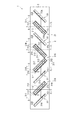
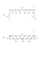
図1は第1実施形態の概略を示す。
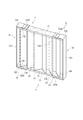
図1において、第1実施形態の偏光変換ユニット1は、偏光変換素子2と、この偏光変換素子2を保持する保持部材3とを備える。保持部材3は平面矩形状の例えば合成樹脂製の板材である。
偏光変換素子2は交互に配置される偏光分離素子21及び反射素子22を備え、これらの偏光分離素子21と反射素子22とのそれぞれの一端部は、保持部材3の凹部(図示せず)に嵌合されている。
偏光分離素子21及び反射素子22は、図1中、保持部材3の中心を挟んで左右に複数枚、例えば、2枚ずつ配置され、このうち、中心に対して左側に配置された偏光分離素子21及び反射素子22と右側に配置された偏光分離素子21及び反射素子22とは、前記中心に対して対称関係に配置されている。
Embodiments of the present invention will be described with reference to the drawings. Here, in each embodiment, the same component is denoted by the same reference numeral, and description thereof is omitted or simplified.
1 to 4 show a first embodiment.
FIG. 1 shows an outline of the first embodiment.
In FIG. 1, the
The
In FIG. 1, a plurality of, for example, two
偏光分離素子21は、その入射側主表面及び出射側主表面が入射光ILに対して所定角度、本実施形態では、略45degをなすように配置された1枚の透光性基板21Aと、この透光性基板21Aの入射側表面に、入射光ILを、互いに直交する第1の直線偏光であるP偏光Pと第2の直線偏光であるS偏光Sとに分離して、P偏光Pを透過させ、S偏光Sを反射する偏光分離部21Bと、この偏光分離部21Bが配置された透光性基板21Aの入射光ILが入射する側の主面とは反対側の主面(出射側の主面)にそれぞれ設けられた反射防止部21Cとを有する。
透光性基板21Aは、複屈折性と旋光性を有する水晶からなる1/2波長板であり、かつ、偏光分離部21Bを透過して入射したP偏光Pを、反射素子22で反射されたS偏光Sの偏波面と平行になるように変換してS偏光Sとして出射するものである。
偏光分離部21Bは、例えば、酸化ケイ素(SiO2)よりなる低屈折率層と、例えば酸化アルミナ(Al2O3)よりなる高屈折率層とが所定の順序及び光学膜厚で形成され、光学的に面内均一とされた誘電体多層膜から構成される。
反射防止部21Cは、例えば、二酸化ケイ素と、酸化チタンとを交互に順次積層してなる誘電体多層膜、等の物質を蒸着することで形成される。
反射素子22は、水晶板22Aと、この水晶板22Aの表面に設けられたミラー部22Bとを有する。
ミラー部22Bは、例えば、二酸化ケイ素、酸化チタン等の物質を蒸着することで形成される多層膜で構成される。
The
The
The
The
The
The
図2は1/2波長板の光学軸方位を説明するための図である。
図2において、1/2波長板である透光性基板21Aの法線から見た光学軸方位をθ0とし、透光性基板21Aの中を進む光線R1に対する光学軸方位をθ1とし、結晶光学軸POの法線PLと光線R1とのなす角度をθ2とすると、これらの角度には次の関係がなりたつ。
θ0=atan(tanθ1×cosθ2) (A1)
また、透光性基板21Aの屈折率をnc、透光性基板21Aと隣接する層を空気層とし、この空気の屈折率をnaとすると、透光性基板21Aでの屈折角はθ2であるから、スネルの方式により、次の関係がなりたつ。
nasinα=ncsinθ2 (A2)
本実施形態では、透光性基板21Aの無機結晶材料である水晶の屈折率ncは1.54であり、空気の屈折率ncは1.00であり、入射角αは45degであるので、式(A2)から、θ2は27.2degとなる。
さらに、θ2は27.2degであり、θ1は45ddegであるため、式(A1)からθ0は、
θ0=atan(tan(45)×cos(27.2))=41.650
=41.7(deg)
と、算出される。
FIG. 2 is a diagram for explaining the optical axis orientation of the half-wave plate.
In FIG. 2, the optical axis direction viewed from the normal line of the
θ 0 = atan (tan θ 1 × cos θ 2 ) (A1)
Further, the refractive index of the
n a sin α = n c sin θ 2 (A2)
In the present embodiment, the refractive index nc of the crystal is an inorganic crystal material of the
Furthermore, since θ 2 is 27.2 deg and θ 1 is 45 ddeg, from equation (A1), θ 0 is
θ 0 = atan (tan (45) × cos (27.2)) = 41.650
= 41.7 (deg)
And calculated.
本実施形態では、透光性基板21Aが単板であるAタイプの場合であり、透光性基板21Aへの入射角度は45(deg)を中心とし、当該中心から±10(deg)度の範囲の角度で傾いた場合、5(deg)ステップで入射角度を変化させたときの偏光変換効率をシミュレーションにより分析し、所定の波長帯域の偏光変換効率を当該波長帯域で平均化したとき、その平均した偏光変換効率における透過損失を平均で評価した。即ち、本実施形態に係る偏光変換素子を投射型映像装置に搭載したときの透過特性を、
M:500〜600nm帯域では、透過損失を10%以内、
N:400〜700nm帯域では、透過損失を20%以内
という規格に設定し、これらの2つのM,Nの規格を満足するように設計条件を設定する。
Aタイプでは、次の条件(A)を満たすことが条件とされる。
条件(A):設計波長をλ、透光性基板21Aの板厚をto、透光性基板21Aを構成する無機結晶材料の切断角度をZとしたとき、設計波長λ、切断角度Z、板厚toの関係が、式(1)(2)(3)(4)を満足する。
λ ≦-0.1293×Z2 + 22.402×Z- 325.73 ・・・(1)
λ ≧ 0.1199×Z2 - 20.762×Z+ 1348.6 ・・・(2)
to ≦ 5E-06×Z2 - 0.0004×Z- 0.0368 ・・・(3)
to ≧ 2-05×Z2 - 0.0029×Z+ 0.136 ・・・(4)
式(1)(2)は設計波長λと切断角度Zとの関係を示すものであり、このうち、式(1)は上限の関係式であり、式(2)は下限の関係式である。また、式(3)(4)は切断角度Zと板厚toとの関係を示すものであり、このうち、式(3)は上限の関係式であり、式(4)は下限の関係式である。
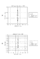
表2は偏光変換効率をシミュレーションにより分析した結果であり、切断角度Zと設計波長λとの関係と切断角度Zと板厚toとの関係が示されている。切断角度Zと設計波長λとの関係が図3(A)にも示され、切断角度Zと板厚toとの関係が図3(B)にも示されている。
In this embodiment, the
M: Transmission loss within 10% in the 500-600nm band,
N: In the 400 to 700 nm band, the transmission loss is set to a standard of 20% or less, and the design conditions are set to satisfy these two M and N standards.
In the A type, the following condition (A) is satisfied.
Condition (A): Design wavelength λ, cutting angle Z, plate, where λ is the design wavelength, to is the plate thickness of the
λ ≦ -0.1293 × Z 2 + 22.402 × Z- 325.73 (1)
λ ≧ 0.1199 × Z 2 - 20.762 × Z + 1348.6 ··· (2)
to ≦ 5E-06 × Z 2 - 0.0004 × Z- 0.0368 ··· (3)
to ≧ 2-05 × Z 2 - 0.0029 × Z + 0.136 ··· (4)
Expressions (1) and (2) show the relationship between the design wavelength λ and the cutting angle Z. Of these, Expression (1) is an upper limit relational expression, and Expression (2) is a lower limit relational expression. . Equations (3) and (4) show the relationship between the cutting angle Z and the plate thickness to, and of these, Equation (3) is the upper relationship, and Equation (4) is the lower relationship. It is.
Table 2 shows the result of analyzing the polarization conversion efficiency by simulation, and shows the relationship between the cutting angle Z and the design wavelength λ and the relationship between the cutting angle Z and the plate thickness to. The relationship between the cutting angle Z and the design wavelength λ is also shown in FIG. 3A, and the relationship between the cutting angle Z and the plate thickness to is also shown in FIG.
表2及び図3(A)(B)から、透過特性を満足させるための設計波長λと切断角度Zの範囲は、
455≦λ≦640(nm)
65≦Z≦110(deg)
である。
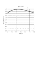
設計波長λと切断角度Zの関係が、上限の関係式である式(3)と、下限の関係式である式(4)とを満足するように設計すれば、例えば、図4に示される通り、前述の透過特性(透過損失)の規格M,Nを満足させることができる。
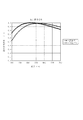
図4は本実施形態で設計した1/2波長板である透光性基板21Aの偏光変換効率が示されている。図4では、太く図示した曲線Lに複数のデータが重ねられて表示されている。
図4で示される通り、偏光変換効率は波長が400nmから700nmまで0.8以上であり、透過損出の平均は20%以内であり、波長が500nmから600nmまでは0.9以上という高い値を示し、透過損出を10%以内とする規格を十分に満足させることができる。
From Table 2 and FIGS. 3A and 3B, the range of the design wavelength λ and the cutting angle Z for satisfying the transmission characteristics is
455 ≦ λ ≦ 640 (nm)
65 ≦ Z ≦ 110 (deg)
It is.
If the design wavelength λ and the cutting angle Z are designed so that the relation (3) which is the upper limit relational expression and the expression (4) which is the lower limit relational expression are satisfied, for example, FIG. As described above, the standards M and N of the transmission characteristics (transmission loss) can be satisfied.
FIG. 4 shows the polarization conversion efficiency of the
As shown in FIG. 4, the polarization conversion efficiency is 0.8 or higher from a wavelength of 400 nm to 700 nm, the average transmission loss is within 20%, and a high value of 0.9 or higher from a wavelength of 500 nm to 600 nm. It is possible to sufficiently satisfy the standard that the transmission loss is within 10%.
以上の構成の第1実施形態では、次の作用効果を奏することができる。
(1)複屈折性と旋光性を有する結晶材料からなる透光性基板21Aと、この透光性基板21Aの入射側表面に設けられP偏光を透過させ、かつ、S偏光を反射する偏光分離部21Bとを備えて偏光分離素子21を構成し、偏光分離部21Bで反射されたS偏光Sを反射する反射素子22を、透光性基板21Aと略平行に離間して配置し、偏光分離部21Bを透過し透光性基板21Aに入射したP偏光Pを、S偏光Sの偏波面と平行となるように変換しS偏光Sとして出射するようにした。そのため、偏光分離素子21と反射素子22とからレンズアレイが構成されていることから、これらの間に設けられたガラス等の透明部材が不要とされ、構造がコンパクトになる。
(2)透光性基板21Aとして結晶材料を用いているため、この結晶材料がガラスに比べて放熱効果が高いので、耐熱性や長寿命化を図ることができる。その上、本実施形態では、透光性基板21Aとして、複屈折性と旋光性を有する無機結晶材料を用いているため、偏光状態が変化して偏光変換効率が低下するという恐れがあるが、偏光分離部21Bを透過し透光性基板21Aに入射したP偏光Pをこの偏波面を維持したまま透光性基板21Aの出射側表面から出射するため、条件(A)、つまり、設計波長λ、切断角度Z、板厚toの関係が、λ ≦-0.1293×Z2 + 22.402×Z- 325.73 ・・・(1)、λ ≧ 0.1199×Z2 - 20.762×Z+ 1348.6 ・・・(2)、to ≦ 5E-06×Z2 - 0.0004×Z- 0.0368・・・(3)及びto ≧ 2-05×Z2 - 0.0029×Z+ 0.136・・・(4)の関係を満足するように設定したから、偏光状態の変化をなくすことができ、光学特性を良好なものにできる。
In the first embodiment having the above configuration, the following operational effects can be achieved.
(1)
(2) Since a crystal material is used as the light-transmitting
(3)1つの偏光分離素子21について透光性基板21Aが1枚であり、透光性基板21Aの法線から見た光学軸方位をθ0とし、透光性基板21Aの中を進む光線に対する光学軸方位をθ1とし、この光線と結晶光学軸POの法線PLとのなす角度をθ2とし、透光性基板21Aの屈折率をnc、透光性基板21Aと隣接する空気層の屈折率をnaとすると、光学軸方位θ0はθ0=atan(tanθ1×cosθ2)(A1)、nasinα=ncsinθ2(A2)、の式から求められるから、透光性基板21Aが1つの偏光分離素子21につき1枚からなる場合において、変換効率の良好な偏光変換素子2を簡易に提供することができる。
(3) light-
(4)透光性基板21Aを、入射光ILに対して45(deg)あるいは135(deg)として配置したから、偏光分離素子21の偏光分離部21BによってS偏光Sを入射光に対して略直角に反射素子22に向けて反射させることができるので、反射素子22で反射される光S偏光Sを透光性基板21Aで出射されるS偏光Sと略平行にすることができる。そのため、反射素子22の反射光と偏光分離素子21の透過光とを容易に揃えることができるので、偏光変換素子2を容易に組み立てることができる。
(4) Since the
(5)透光性基板21Aは水晶から形成されるので、水晶がサファイヤ等の他の結晶材料に比べて安価に入手できるから、偏光変換素子2を安価に提供することができる。
(6)反射素子22において、ミラー部22Bが設けられる板材がガラスではなく水晶であるため、偏光分離素子21とともに反射素子22でも、放熱効果が高くなり、耐熱性や長寿命化を一層図ることができる。
(7)偏光分離部21Bは誘電体多層膜で構成されるから、簡単に偏光分離素子21を製造することができる。
(5) Since the
(6) In the
(7) Since the
次に、本発明の第2実施形態を図5から図8に基づいて説明する。
第2実施形態は透光性基板21Aを2枚の位相差板から構成した点に特徴があり、他の構成は第1実施形態と同じである。
図5には本発明の第2実施形態にかかる偏光変換素子の概略が示されている。
図5において、透光性基板21Aは、それぞれ水晶からなる板状の第1の無機結晶材料211と、第2の無機結晶材料212とから構成され、第1の無機結晶材料211は、その一面に反射防止部21Cが形成される。この反射防止部21Cには偏光分離部21Bが設けられている。第1の無機結晶材料211の他面には第2の無機結晶材料212の一面が対向され、この第2の無機結晶材料の他面には反射防止部21Cが形成される。なお、図5では、第1の無機結晶材料211と第2の無機結晶材料212とが接着層213で互いに接着されている構成が示されているが、本実施形態では、第1の無機結晶材料211と第2の無機結晶材料212とを単に積層する構成としてもよい。
Next, a second embodiment of the present invention will be described with reference to FIGS.
The second embodiment is characterized in that the
FIG. 5 schematically shows a polarization conversion element according to the second embodiment of the present invention.
In FIG. 5, the
本実施形態では、透光性基板21Aの光学軸方位が図6に示される。
図6に示される通り、第1の無機結晶材料211と第2の無機結晶材料212との結晶光学軸PO1,PO2が互いに交差するように接着層213で貼り合わされる。本実施形態では、透光性基板21Aが第1の無機結晶材料211と第2の無機結晶材料212とを貼り合わせてなる通称Dタイプの位相差板である。
第1の無機結晶材料211の光学軸方位θ01と第2の無機結晶材料212の光学軸方位θ02とは次の式から求められる。
つまり、透光性基板21Aの法線から見た第1の無機結晶材料211の光学軸方位をθ01とし、第1の無機結晶材料211の中を進む光線R1に対する光学軸方位をθ11とし、この光線R1と結晶光学軸PO1の法線とのなす角度をθ21(図6での図示省略)とし、第1の無機結晶材料211の屈折率をnc1、第1の無機結晶材料211と隣接する空気層の屈折率をnaとすると、第1の無機結晶材料211の光学軸方位θ01は
θ01=atan(tanθ11×cosθ21) (A11)
nasinα=nc1sinθ21 (A21)
の式から求められる。
In the present embodiment, the optical axis orientation of the
As shown in FIG. 6, the first
The optical axis direction θ 01 of the first
That is, the optical axis direction of the first
θ 01 = atan (tan θ 11 × cos θ 21 ) (A11)
n a sin α = n c1 sin θ 21 (A21)
It can be obtained from the following formula.
同様に、第2の無機結晶材料212の中を進む光線に対する光学軸方位をθ12とし、光線と結晶光学軸PO2の法線とのなす角度をθ22(図6での図示省略)とし、第2の無機結晶材料212の屈折率をnc2、第2の無機結晶材料212と隣接する第1の無機結晶材料211の屈折率をnc1とすると、
第2の無機結晶材料212の光学軸方位θ02は
θ02=atan(tanθ12×cosθ22) (A12)
nc1sinθ21=nc2sinθ22 (A22)
の式から求められる。
ここで、本実施形態では、光学軸方位θ12と光学軸方位θ11との差が90degである。
Similarly, the optical axis direction with respect to the light beam traveling in the second
The optical axis orientation θ 02 of the second
θ 02 = atan (tan θ 12 × cos θ 22 ) (A12)
n c1 sinθ 21 = n c2 sinθ 22 (A22)
It can be obtained from the following formula.
Here, in the present embodiment, the difference between the optical axis direction θ 12 and the optical axis direction θ 11 is 90 deg.
第1の無機結晶材料211と第2の無機結晶材料212の材料である水晶の屈折率nc1,nc2は1.54であり、空気の屈折率naは1.00であり、入射角αは45degである。さらに、光学軸方位θ11は45degであり、光学軸方位θ12は135deg(45deg+90deg)であるから(例えば、特開昭58−194004号、特開昭59−062807号)、式(A11)(A21)(A12)(A22)から、光学軸方位θ01,θ02を求めることができる。
光学軸方位θ01は、
nasinα=nc1sinθ21 (A21)
1.00×sin45deg=1.54×sinθ21
0.7071=1.54×sinθ21
θ21=27.32deg
θ01=atan(tanθ11×cosθ21) (A11)
=atan(tan45deg×cos27.32deg)
=atan(0.89)
=41.7(deg)
光学軸方位θ02は、
nc1sinθ21=nc2sinθ22 (A22)
1.54sin27.32deg=1.54sinθ22
θ22=27.32deg
θ02=atan(tanθ12×cosθ22) (A12)
=atan(tan135deg×cos27.32deg)
=atan(−0.888)
=−41.7(deg)
光学軸方位θ02の−41.7degを図6の図示に合わせるとθ02は138.3degとなる。
A first inorganic
The optical axis direction θ 01 is
n a sin α = n c1 sin θ 21 (A21)
1.00 × sin45deg = 1.54 × sinθ 21
0.7071 = 1.54 × sinθ 21
θ 21 = 27.32 deg
θ 01 = atan (tan θ 11 × cos θ 21 ) (A11)
= Atan (tan45deg × cos27.32deg)
= Atan (0.89)
= 41.7 (deg)
The optical axis direction θ 02 is
n c1 sinθ 21 = n c2 sinθ 22 (A22)
1.54sin27.32deg = 1.54sinθ 22
θ 22 = 27.32 deg
θ 02 = atan (tan θ 12 × cos θ 22 ) (A12)
= Atan (tan135deg × cos27.32deg)
= Atan (−0.888)
= -41.7 (deg)
When −41.7 deg of the optical axis azimuth θ 02 is matched with the illustration in FIG. 6, θ 02 becomes 138.3 deg.
本実施形態では、第1実施形態と同様に、透光性基板21Aへの入射角度は45(deg)を中心とし、当該中心から±10(deg)度の範囲の角度で傾いた場合、5(deg)ステップで入射角度を変化させたときの偏光変換効率をシミュレーションにより分析し、所定の波長帯域の偏光変換効率を当該波長帯域で平均化したとき、その平均した偏光変換効率における透過損失を平均で評価した。即ち、本実施形態に係る偏光変換素子を投射型映像装置に搭載したときの透過特性を、
M:500〜600nm帯域では、透過損失を10%以内、
N:400〜700nm帯域では、透過損失を20%以内
という規格に設定し、これらの2つの規格を満足するように設計条件を設定する。
Dタイプと通称される本実施形態の位相差板では、次の条件(B)を満たすことが条件とされる。
条件(B):設計波長λ、前記透光性基板の板厚to、前記無機結晶材料の切断角度をZとしたとき、設計波長λ、切断角度Z及び板厚toの関係が、式(5)(6)(7)(8)(9)を満足し、
λ ≦ -10.75×Z2 + 1933.9×Z- 86330 ・・・(5)
λ ≧ 6.25×Z2 - 1126.6×Z+ 51216 ・・・(6)
to ≦-0.0281×Z2 + 5.0512×Z- 225.61 ・・・(7)
to ≧ 0.0173×Z2 - 3.1146×Z+ 141.39 ・・・(8)
ここで、前記板厚toは、前記第1の無機結晶材料211と前記第2の無機結晶材料212とを貼り合わせてなる位相差板の板厚で定義されている。即ち、前記第1の無機結晶材料211の板厚t211と前記第2の無機結晶材料212の板厚t212との合計の板厚となっている。
透光性基板21A中を進む光線の進行方向における2枚の無機結晶材料のうち第1の無機結晶材料211の位相差をΓ1、第2の無機結晶材料212の位相差をΓ2としたときに下式を満足する。
|Γ1−Γ2|=180(deg) ・・・(9)
式(5)(6)は設計波長λと切断角度Zとの関係を示すものであり、このうち、式(5)は上限の関係式であり、式(6)は下限の関係式である。また、式(7)(8)は切断角度Zと板厚toとの関係を示すものであり、このうち、式(7)は上限の関係式であり、式(8)は下限の関係式である。
表3は偏光変換効率をシミュレーションにより分析した結果であり、切断角度Zと設計波長λとの関係と切断角度Zと板厚toとの関係が示されている。切断角度Zと設計波長λとの関係が図7(A)にも示され、切断角度Zと板厚toとの関係が図7(B)にも示されている。
In the present embodiment, as in the first embodiment, the incident angle to the
M: Transmission loss within 10% in the 500-600nm band,
N: In the 400 to 700 nm band, the transmission loss is set to a standard of 20% or less, and the design conditions are set to satisfy these two standards.
In the phase difference plate of the present embodiment, commonly referred to as D type, the following condition (B) is satisfied.
Condition (B): When the design wavelength λ, the plate thickness to of the translucent substrate, and the cutting angle of the inorganic crystal material are Z, the relationship between the design wavelength λ, the cutting angle Z and the plate thickness to ) (6) (7) (8) (9)
λ ≤ -10.75 × Z 2 + 1933.9 × Z-86330 (5)
λ ≧ 6.25 × Z 2 - 1126.6 × Z + 51216 ··· (6)
to ≦ -0.0281 × Z 2 + 5.0512 × Z- 225.61 (7)
to ≧ 0.0173 × Z 2 - 3.1146 × Z + 141.39 ··· (8)
Here, the plate thickness to is defined by the plate thickness of a retardation plate formed by bonding the first
When the phase difference of the first
| Γ1-Γ2 | = 180 (deg) (9)
Expressions (5) and (6) show the relationship between the design wavelength λ and the cutting angle Z. Of these, Expression (5) is an upper limit relational expression, and Expression (6) is a lower limit relational expression. . Expressions (7) and (8) show the relationship between the cutting angle Z and the plate thickness to, among which Expression (7) is the upper limit relational expression and Expression (8) is the lower limit relational expression. It is.
Table 3 shows the result of analyzing the polarization conversion efficiency by simulation, and shows the relationship between the cutting angle Z and the design wavelength λ and the relationship between the cutting angle Z and the plate thickness to. The relationship between the cutting angle Z and the design wavelength λ is also shown in FIG. 7A, and the relationship between the cutting angle Z and the plate thickness to is also shown in FIG. 7B.
表3及び図7(A)(B)から、透過特性を満足させるための設計波長λと切断角度Zの範囲は、
450≦λ≦640(nm)
87≦Z≦93(deg)
である。
設計波長λと切断角度Zの関係が、上限の関係式である式(5)と、下限の関係式である式(6)とを満足するように設計すれば、例えば、図8に示される通り、前述の透過特性(透過損失)の規格M,Nを満足させることができる。
図8は本実施形態で設計した1/2波長板である透光性基板21Aの偏光変換効率が示されている。図8では、太く図示した曲線Lに複数のデータが含まれる。
図8で示される通り、偏光変換効率は波長が400nmから700nmまで0.8以上であって、透過損出の平均は20%以内であり、波長が500nmから600nmまでは0.9以上という高い値を示し、透過損出を10%以内とする規格を十分に満足させることができる。
そのため、第1の無機結晶材料211の板厚m1を0.048mmとし、波長を520nmとすると、第1の無機結晶材料211の位相差は270degであり、第2の無機結晶材料212の板厚m2を0.020mmとし、波長を520nmとすると、第2の無機結晶材料212の位相差は110degである。
From Table 3 and FIGS. 7A and 7B, the range of the design wavelength λ and the cutting angle Z for satisfying the transmission characteristics is
450 ≦ λ ≦ 640 (nm)
87 ≦ Z ≦ 93 (deg)
It is.
If the design wavelength λ and the cutting angle Z are designed so that the relation (5) which is the upper limit relation and the expression (6) which is the lower limit relation are satisfied, for example, FIG. As described above, the standards M and N of the transmission characteristics (transmission loss) can be satisfied.
FIG. 8 shows the polarization conversion efficiency of the
As shown in FIG. 8, the polarization conversion efficiency is 0.8 or higher from 400 nm to 700 nm, the average transmission loss is within 20%, and is 0.9 or higher from 500 nm to 600 nm. It is possible to sufficiently satisfy the standard showing a value and a transmission loss within 10%.
Therefore, if the plate thickness m 1 of the first
従って、第2実施形態では、第1実施形態の(1)(3)〜(7)と同様の作用効果を奏する他、次の作用効果を奏することができる。
(8)本実施形態では、偏光分離部21Bを透過し透光性基板21Aに入射したP偏光Pをこの偏波面を維持したまま透光性基板21Aの出射側表面から出射するため、設計波長λ、透光性基板21Aの板厚to、無機結晶材料の切断角度をZとしたとき、設計波長λ、切断角度Z及び板厚toの関係が、条件(B)、つまり、λ ≦ -10.75×Z2 + 1933.9×Z- 86330 ・・・(5)、λ ≧ 6.25×Z2 - 1126.6×Z+ 51216・・・(6)、to ≦-0.0281×Z2 + 5.0512×Z- 225.61・・・(7)、to ≧ 0.0173×Z2 - 3.1146×Z+ 141.39・・・(8)、第1の無機結晶材料212の位相差をΓ1、第2の無機結晶材料212の位相差をΓ2としたときに、|Γ1−Γ2|=180(deg)・・・(9)の関係を満足するように設定したから、偏光状態の変化をなくすことができ、光学特性を良好なものにできる。
Therefore, in 2nd Embodiment, there can exist the following effect other than the same effect as (1) (3)-(7) of 1st Embodiment.
(8) In the present embodiment, the P-polarized light P that has passed through the
(9)透光性基板21Aを第1の無機結晶材料211と第2の無機結晶材料212との2枚から構成し、透光性基板21Aの法線から見た第1の無機結晶材料211の光学軸方位をθ01とし、第1の無機結晶材料211の中を進む光線に対する光学軸方位をθ11とし、この光線と結晶光学軸PO1の法線とのなす角度をθ21とし、第1の無機結晶材料211の屈折率をnc1、第1の無機結晶材料211と隣接する空気層の屈折率をnaとすると、第1の無機結晶材料211の光学軸方位θ01はθ01=atan(tanθ11×cosθ21)(A11)、nasinα=nc1sinθ21(A21)の式から求められ、透光性基板21Aの法線から見た第2の無機結晶材料212の光学軸方位をθ02とし、第2の無機結晶材料212の中を進む光線に対する光学軸方位をθ12とし、この光線と結晶光学軸PO2の法線とのなす角度をθ22とし、第2の無機結晶材料212の屈折率をnc2、第2の無機結晶材料212と隣接する第1の無機結晶材料211の屈折率をnc1とすると、第2の無機結晶材料212の光学軸方位θ02はθ02=atan(tanθ12×cosθ22)(A12)、nC1sinθ21=nc2sinθ22(A22)の式から求められるから、透光性基板21Aが第1の無機結晶材料211と第2の無機結晶材料212とからなる位相差板の場合において、変換効率の良好な偏光変換素子を簡易に提供することができる。
(9) The
次に、本発明の第3実施形態を図5、図9、図10に基づいて説明する。
図5に示される通り、第3実施形態では、透光性基板21Aが2枚の第1の無機結晶材料211と第2の無機結晶材料212とからなる点では第2実施形態と同じであるが、第1の無機結晶材料211と第2の無機結晶材料212との具体的な構成が第2実施形態と異なる。
図9には、第3実施形態の透光性基板21Aの光学軸方位が示されている。
図9において、第3実施形態の透光性基板21Aは、1/2波長板であり、第1の無機結晶材料211と第2の無機結晶材料212とを結晶光学軸PO1,PO2が互いに交差するよう重ね合わせたものである。
Next, a third embodiment of the present invention will be described based on FIG. 5, FIG. 9, and FIG.
As shown in FIG. 5, the third embodiment is the same as the second embodiment in that the
FIG. 9 shows the optical axis orientation of the
In FIG. 9, the
本実施形態では、透光性基板21Aが第1の無機結晶材料211と第2の無機結晶材料212とを貼り合わせてなる通称WB1タイプと称される広域帯の位相差板の場合であり、第1の無機結晶材料211の光学軸方位θ01と、第2の無機結晶材料212の光学軸方位θ02とは第2実施形態と同様に求められる。但し、本実施形態では、光学軸方位θ11と光学軸方位θ12との和が90degである。
第1の無機結晶材料211と第2の無機結晶材料212の材料である水晶の屈折率nc1,nc2は1.54であり、空気の屈折率naは1.00であり、光学軸方位θ11は22.5degであり、光学軸方位θ12は67.5deg(=90deg−22.5deg)であり、入射角αは45degである。式(A11)(A21)(A12)(A22)から、光学軸方位θ01,θ02を求めることができる。
光学軸方位θ01は、
nasinα=nc1sinθ21 (A21)
1.00×sin45deg=1.54×sinθ21
0.7071=1.54×sinθ21
θ21=27.32deg
θ01=atan(tanθ11×cosθ21) (A11)
=atan(tan45deg×cos27.32deg)
=atan(0.89)
=41.7(deg)
光学軸方位θ02は、
nc1sinθ21=nc2sinθ22 (A22)
1.54sin27.32deg=1.54sinθ22
θ22=27.32deg
θ02=atan(tanθ12×cosθ22) (A12)
=atan(tan67.5deg×cos27.32deg)
=atan(2.14)
=65.0(deg)
In the present embodiment, the
A first inorganic
The optical axis direction θ 01 is
n a sin α = n c1 sin θ 21 (A21)
1.00 × sin45deg = 1.54 × sinθ 21
0.7071 = 1.54 × sinθ 21
θ 21 = 27.32 deg
θ 01 = atan (tan θ 11 × cos θ 21 ) (A11)
= Atan (tan45deg × cos27.32deg)
= Atan (0.89)
= 41.7 (deg)
The optical axis direction θ 02 is
n c1 sinθ 21 = n c2 sinθ 22 (A22)
1.54sin27.32deg = 1.54sinθ 22
θ 22 = 27.32 deg
θ 02 = atan (tan θ 12 × cos θ 22 ) (A12)
= Atan (tan 67.5 deg × cos 27.32 deg)
= Atan (2.14)
= 65.0 (deg)
第3実施形態では、前記各実施形態と同様に、透光性基板21Aへの入射角度は45(deg)を中心とし、当該中心から±10(deg)度の範囲の角度で傾いた場合、5(deg)ステップで入射角度を変化させたときの偏光変換効率をシミュレーションにより分析し、所定の波長帯域の偏光変換効率を当該波長帯域で平均化したとき、その平均した偏光変換効率における透過損失を平均で評価した。即ち、本実施形態に係る偏光変換素子を投射型映像装置に搭載したときの透過特性を、
M:500〜600nm帯域では、透過損失を10%以内、
N:400〜700nm帯域では、透過損失を20%以内
という規格に設定し、これらの2つの規格を満足するように設計条件を設定する。
WB1タイプと通称される広帯域位相差板では、次の条件(C)を満たすことが条件とされる。
条件(C):設計波長λ、前記透光性基板の板厚to、前記無機結晶材料の切断角度をZとしたとき、設計波長λ、切断角度Z及び板厚toの関係が、式(10)(11)(12)(13)を満足する。
λ≦-2E-07×Z6+ 0.0001×Z5 -0.024×Z4 +2.7749×Z3 -178.61×Z2 + 6067.8×Z - 84312 ・・・(10)
λ≧ -4E-05×Z3+ 0.0757×Z2 - 10.073×Z + 696.9 ・・・(11)
to≦-2E-08×Z4 + 6E-06×Z3 - 0.0008×Z2 + 0.0495×Z - 0.9844・・・(12)
to≧5E-07×Z3 - 0.0001×Z2 + 0.0065×Z - 0.0924・・・(13)
ここで、前記板厚toは、第2実施形態と同様に、前記第1の無機結晶材料211と前記第2の無機結晶材料212とを貼り合わせてなる位相差板の板厚で定義されている。即ち、前記第1の無機結晶材料211の板厚t211と前記第2の無機結晶材料212の板厚t212との合計の板厚となっている。
式(10)(11)は設計波長λと切断角度Zとの関係を示すものであり、このうち、式(10)は上限の関係式であり、式(11)は下限の関係式である。また、式(12)(13)は切断角度Zと板厚toとの関係を示すものであり、このうち、式(12)は上限の関係式であり、式(13)は下限の関係式である。
表4は偏光変換効率をシミュレーションにより分析した結果であり、切断角度Zと設計波長λとの関係と切断角度Zと板厚toとの関係が示されている。切断角度Zと設計波長λとの関係が図10(A)にも示され、切断角度Zと板厚toとの関係が図10(B)にも示されている。
In the third embodiment, as in each of the embodiments described above, when the incident angle to the
M: Transmission loss within 10% in the 500-600nm band,
N: In the 400 to 700 nm band, the transmission loss is set to a standard of 20% or less, and the design conditions are set to satisfy these two standards.
The broadband retardation plate commonly referred to as the WB1 type is required to satisfy the following condition (C).
Condition (C): When the design wavelength λ, the plate thickness to of the translucent substrate, and the cutting angle of the inorganic crystal material are Z, the relationship between the design wavelength λ, the cutting angle Z and the plate thickness to ) (11) (12) (13) is satisfied.
λ ≦ −2E-07 × Z 6 + 0.0001 × Z 5 −0.024 × Z 4 + 2.7749 × Z 3 −178.61 × Z 2 + 6067.8 × Z −84312 (10)
λ ≧ -4E-05 × Z 3 + 0.0757 × Z 2 - 10.073 × Z + 696.9 ··· (11)
to ≦ -2E-08 × Z 4 + 6E-06 × Z 3 - 0.0008 ×
to ≧ 5E-07 × Z 3 - 0.0001 ×
Here, the plate thickness to is defined by the plate thickness of a retardation plate formed by bonding the first
Expressions (10) and (11) show the relationship between the design wavelength λ and the cutting angle Z. Of these, Expression (10) is an upper limit relational expression, and Expression (11) is a lower limit relational expression. . Expressions (12) and (13) show the relationship between the cutting angle Z and the plate thickness to, among which, Expression (12) is the upper limit relational expression, and Expression (13) is the lower limit relational expression. It is.
Table 4 shows the result of analyzing the polarization conversion efficiency by simulation, and shows the relationship between the cutting angle Z and the design wavelength λ and the relationship between the cutting angle Z and the plate thickness to. The relationship between the cutting angle Z and the design wavelength λ is also shown in FIG. 10A, and the relationship between the cutting angle Z and the plate thickness to is also shown in FIG. 10B.
表4及び図10(A)(B)から、透過特性を満足させるための設計波長λと切断角度Zの範囲は、
450≦λ≦640(nm)
87≦Z≦93(deg)
である。
設計波長λと切断角度Zの関係が、上限の関係式である式(10)と、下限の関係式である式(11)とを満足するように設計すれば、例えば、図11に示される通り、前述の透過特性(透過損失)の規格M,Nを満足させることができる。
図11は本実施形態で設計した1/2波長板である透光性基板21Aの偏光変換効率が示されている。図11では、太く図示した曲線Lに複数のデータが含まれる。
図11で示される通り、偏光変換効率は波長が400nmから700nmまで0.8以上(0.9以上)であって、透過損出の平均は20%以内であり、波長が500nmから600nmまでは0.9以上(1.0に極めて近い)という高い値を示し、透過損出を10%以内とする規格を十分に満足させることができる。
そのため、第1の無機結晶材料211の板厚m1を0.048mmとし、波長を520nmとすると、第1の無機結晶材料211の位相差は270degであり、第2の無機結晶材料212の板厚m2を0.020mmとし、波長を520nmとすると、第2の無機結晶材料212の位相差は110degである。
From Table 4 and FIGS. 10A and 10B, the range of the design wavelength λ and the cutting angle Z for satisfying the transmission characteristics is
450 ≦ λ ≦ 640 (nm)
87 ≦ Z ≦ 93 (deg)
It is.
If the design wavelength λ and the cutting angle Z are designed so that the relation (10) which is the upper limit relational expression and the expression (11) which is the lower limit relational expression are satisfied, for example, FIG. As described above, the standards M and N of the transmission characteristics (transmission loss) can be satisfied.
FIG. 11 shows the polarization conversion efficiency of the
As shown in FIG. 11, the polarization conversion efficiency is 0.8 or more (0.9 or more) from a wavelength of 400 nm to 700 nm, the average transmission loss is within 20%, and the wavelength is from 500 nm to 600 nm. It shows a high value of 0.9 or more (very close to 1.0), and can sufficiently satisfy the standard that the transmission loss is within 10%.
Therefore, if the plate thickness m 1 of the first
従って、第3実施形態では、第2実施形態の(1)(3)〜(7)(9)と同様の作用効果を奏する他、次の作用効果を奏することができる。
(10)偏光分離部21Bを透過し透光性基板21Aに入射したP偏光Pをこの偏波面を維持したまま透光性基板21Aの出射側表面から出射するために、設計波長λ、透光性基板21Aの板厚to、無機結晶材料の切断角度をZとしたとき、設計波長λ、切断角度Z及び板厚toの関係が、条件(C)、つまり、λ≦-2E-07×Z6+ 0.0001×Z5 -0.024×Z4 +2.7749×Z3 -178.61×Z2 + 6067.8×Z - 84312・・(10)、λ≧-4E-05×Z3+ 0.0757×Z2-10.073×Z + 696.9・・(11)、to≦-2E-08×Z4 + 6E-06×Z3 - 0.0008×Z2+ 0.0495×Z -0.9844・・(12)、to≧5E-07×Z3-0.0001×Z2 + 0.0065×Z -0.0924・・・(13)を満足するように設定したから、偏光状態の変化をなくすことができ、光学特性を良好なものにできる。
Therefore, in the third embodiment, the following operational effects can be achieved in addition to the same operational effects as (1), (3) to (7), and (9) of the second embodiment.
(10) In order to emit the P-polarized light P transmitted through the
次に、本発明の第4実施形態を図12から図15に基づいて説明する。
第4実施形態は偏光変換ユニット4を投影型映像装置である液晶プロジェクター100に設けた例であり、第1実施形態の変換ユニット1とは保持部材5の構造が異なる。
図12は液晶プロジェクターの概略構成を示す。
図12において、液晶プロジェクター100は、インテグレーター照明光学系110と、色分離光学系120と、リレー光学系130と、光源から射出された光を画像情報に応じて変調する光変調装置140と、光変調装置140で変調された光を拡大投射する投写光学装置150とを備える。
インテグレーター照明光学系110は、後述する3枚の透過型液晶パネル141R,141G,141Bの画像形成領域をほぼ均一に照明するための光学系であり、光源装置111と、第1レンズアレイ112と、偏光変換装置200と、重畳レンズ113とを備える。
Next, a fourth embodiment of the present invention will be described with reference to FIGS.
The fourth embodiment is an example in which the
FIG. 12 shows a schematic configuration of the liquid crystal projector.
In FIG. 12, a
The integrator illumination
光源装置111は、光源ランプ114から射出された輻射状の光線をリフレクター115で反射して略平行光線とし、この略平行光線を外部へと射出する。
偏光変換装置200は、第2レンズアレイ210と、遮光板220と、第2実施形態にかかる偏光変換ユニット4とを備える。
色分離光学系120は、2枚のダイクロイックミラー121,122と、反射ミラー123とを備え、ダイクロイックミラー121、122によりインテグレーター照明光学系110から射出された複数の光を赤、緑、青の3色の色光に分離する。ダイクロイックミラー121で分離された青色光は、反射ミラー123によって反射され、フィールドレンズ142を通って、青色用の透過型液晶パネル141Bに到達する。
ダイクロイックミラー121を透過した赤色光と緑色光のうちで、緑色光は、ダイクロイックミラー122によって反射され、フィールドレンズ142を通って、緑色用の透過型液晶パネル141Gに到達する。
リレー光学系130は、入射側レンズ131と、リレーレンズ133と、反射ミラー132、134とを備える。色分離光学系120で分離された赤色光は、ダイクロイックミラー122を透過して、リレー光学系130を通り、さらにフィールドレンズ142を通って、赤色光用の透過型液晶パネル141Rに到達する。
光変調装置140は、透過型液晶パネル141R,141G,141Bと、クロスダイクロイックプリズム143とを備える。このクロスダイクロイックプリズム143は、各色光に変調された光学像を合成してカラーの光学像を形成するものである。
The
The
The color separation
Of the red light and green light transmitted through the
The relay
The
偏光変換ユニット4は、第1実施形態と同じ構造の偏光変換素子2と、この偏光変換素子2を保持する保持部材5とを備える。
保持部材5の具体的な構造が図13から図15に示されている。
図13は保持部材5の斜視図、図14(A)は保持部材5の平面図、図14(B)は保持部材5の断面図である。
これらの図において、保持部材5は、偏光分離素子21の両端部と反射素子22の両端部とをそれぞれ保持する一対の保持板51と、これらの一対の保持板51の両端部をそれぞれ連結する一対の連結板52とを有する構造である。これらの保持板51及び連結板52は合成樹脂から一体に平面矩形の枠状に形成されている。
一対の保持板51の互いに対向する部分には、偏光分離素子21と反射素子22とをそれぞれ案内するガイド溝51Aが複数対形成されている。これらのガイド溝51Aは、その長手方向が入射光に対して45degまたは135degとなるように形成されている。
The
The specific structure of the holding
13 is a perspective view of the holding
In these drawings, the holding
A plurality of pairs of
なお、図13及び図14において、ガイド溝51Aは、偏光分離素子21を収納するために4対が図示され、反射素子22を収納するために2対が図示されているが、これは、ガイド溝51Aの構成をわかりやすくするために拡大図示したためであり、実際は、図1に示される偏光変換素子2に合わせて、4枚の偏光分離素子21を収納するために4対が設けられ、4枚の反射素子22を収納するために4対が設けられる構造である。ただし、ガイド溝51Aの数は前述のものに限定されるものではなく、実際に設けられる偏光分離素子21や反射素子22の数に対応する。
In FIG. 13 and FIG. 14, four pairs of
図15は保持部材5の一部の分解斜視図である。図15において、ガイド溝51Aは、一端部が保持板51の一側面に開口され、他端部が偏光分離素子21や反射素子22の端部が突き当たるように段差が形成されている。ガイド溝51Aは、その幅寸法が偏光分離素子21や反射素子22の幅寸法と同じあるいはやや大きく形成され、その長さ寸法が偏光分離素子21や反射素子22の長さ寸法と同じあるいはやや大きく形成されている。
FIG. 15 is an exploded perspective view of a part of the holding
従って、第4実施形態では、第1実施形態の(1)から(6)までの作用効果と同様の作用効果を奏することができる他に、次の作用効果を奏することができる。
(11)光源装置111からの光をS偏光Sに変換して出射する偏光変換素子2を有する偏光変換ユニット4と、偏光変換素子2からの出射光を画像情報に応じて変調する光変調装置140と、この光変調装置140により変調された光を投写する投写光学装置150とを備えて液晶プロジェクター100を構成したから、偏光変換素子2の偏光変換効率が高いことに伴って液晶プロジェクター100の投影精度を高いものにできる。
Therefore, in 4th Embodiment, in addition to the effect similar to the effect from (1) to (6) of 1st Embodiment, there can exist the following effect.
(11) A
(12)光変調装置140は、透過型液晶パネル141R,141G,141Bを備えて構成されるので、この点からも、投影精度の高い液晶プロジェクター100を提供することができる。
(13)偏光変換ユニット4は、偏光変換素子2を保持する保持部材5を備え、この保持部材5は、偏光分離素子21の両端部と反射素子22の両端部とをそれぞれ保持する一対の保持板51と、これらの一対の保持板51の両端部をそれぞれ連結する一対の連結板52とを有する構造であるため、偏光分離素子21及び反射素子22を保持部材にコンパクトに収納することができ、取り扱いが便利となる。
(12) Since the
(13) The
(14)一対の保持板51と一対の連結板52とが一体に形成されているので、射出成形等の適宜な手段によって、保持部材5を容易に製造することができる。
(15)一対の保持板51の互いに対向する部分には偏光分離素子21と反射素子22とをそれぞれ案内するガイド溝51Aが形成され、これらのガイド溝は一対の保持板51の一側面にそれぞれ開口されているので、偏光分離素子21と反射素子22とをそれぞれガイド溝51Aに沿って差し込むだけで偏光変換ユニット4が組み立てられることになり、組立作業が容易となる。
(14) Since the pair of holding
(15)
次に、本発明の第5実施形態を図16及び図17に基づいて説明する。
第5実施形態は保持部材の構造が第4実施形態とは異なるもので、他の構成は第4実施形態と同じである。
図16は第5実施形態にかかる偏光変換ユニットを示す斜視図であり、図17は保持部材の一部を示す分解斜視図である。
これらの図において、偏光変換ユニット6は第1実施形態と同じ構造の偏光変換素子2と、この偏光変換素子2を保持する保持部材7とを備える。
保持部材7は、一対の保持板71と、一対の保持板71の端部に設けられた一対の連結板72とを備え、一対の保持板71と一対の連結板72とは別体に形成されている。
Next, a fifth embodiment of the present invention will be described with reference to FIGS.
In the fifth embodiment, the structure of the holding member is different from that of the fourth embodiment, and other configurations are the same as those of the fourth embodiment.
FIG. 16 is a perspective view showing a polarization conversion unit according to the fifth embodiment, and FIG. 17 is an exploded perspective view showing a part of a holding member.
In these drawings, the
The holding
一対の保持板71は合成樹脂から形成された板状であり、その互いに対向する部分には、偏光分離素子21と反射素子22との端部をそれぞれガイドするガイド溝71Aが複数対形成されている。これらのガイド溝71Aは、その長手方向が入射光に対して45degまたは135degとなるように形成されている。そして、ガイド溝71Aは、平面が矩形状とされた凹部である。
第5実施形態では、ガイド溝71Aは、合計6対が図示されているが、実際には、偏光変換素子2に合わせて、4枚の偏光分離素子21を収納するために4対が設けられ、4枚の反射素子22を収納するために4対が設けられる構造である。
The pair of holding
In the fifth embodiment, a total of six pairs of
一対の連結板72は、長尺状の板材721と、この板材721に連結され一対の保持板71を互いに向き合う方向に付勢する係合片722とを有する。
これらの板材721と係合片722とは弾性を有する材料、例えば、金属、合成樹脂等から一体に形成されている。係合片722は板材721に対して折り曲げて形成されており、その中央部分に保持板71に形成された凹部71Bに係合する凸状の抑え部722Aが形成されている。凸状の抑え部722Aと凹部71Bとは保持板71の長手方向と直交する方向に延びて形成されている。
The pair of connecting
The
従って、第5実施形態では、第4実施形態の(1)〜(6)(11)〜(15)までの作用効果と同様の作用効果を奏することができる他に次の作用効果を奏することができる。
(16)保持部材7は、一対の保持板71と、一対の保持板71の端部に設けられた一対の連結板72とを備え、一対の連結板72は、長尺状の板材721と、この板材721に連結され一対の保持板71を互いに向き合う方向に付勢する係合片722とを有する。そのため、一対の連結板72によって、一対の保持板71を互いに近接する方向に付勢するので、偏光分離素子21と反射素子22とを確実に保持部材7で保持することができるから、偏光分離素子21や反射素子22が保持部材7から誤って脱落することがない。
Therefore, in 5th Embodiment, there can exist the following effect other than the effect similar to the effect from (1)-(6) (11)-(15) of 4th Embodiment. Can do.
(16) The holding
(17)係合片722は保持板71に形成された凹部71Bに係合する抑え部722Aを有するので、連結板72が保持板71の長手方向にずれて外れることがない。そのため、保持板71から連結板72が誤って外れることを防止できる。
(18)保持板71に形成され偏光分離素子21や反射素子22の端部が保持されるガイド溝71Aは、平面が矩形状とされた凹部であるため、保持板71の平面内での偏光分離素子21や反射素子22の移動が規制される。そのため、この点からも、偏光分離素子21や反射素子22が保持部材7から誤って脱落することがない。
(17) Since the
(18) Since the
次に、本発明の第6実施形態を図18に基づいて説明する。
第6実施形態は偏光分離素子の構成が第1実施形態と異なるもので、他の構成は第1実施形態と同じである。
図18は第6実施形態にかかる偏光分離素子21の偏光分離部210Bの斜視図である。図18において、偏光分離素子21の偏光分離部210Bは誘電基板21Dによって支持される多数の平行な金属ワイヤーからなる導電電極21Eから形成される。導電電極21Eは、そのピッチまたは周期がPであり、個別の導体の幅がWであり、その厚さがtである。入射光ILは、垂線からの角度Rで偏光分離素子21に入射する。入射光ILは、S偏光Sとして反射し、回折されないで、P偏光Pとして透過される。ここで、周期P、幅W、厚さtは、使用する光の周波数領域、その他条件により設定される。
Next, a sixth embodiment of the present invention will be described with reference to FIG.
The sixth embodiment is different from the first embodiment in the configuration of the polarization separation element, and the other configurations are the same as those in the first embodiment.
FIG. 18 is a perspective view of the
従って、第6実施形態によれば、第1実施形態の(1)〜(6)と同様の作用効果を奏することができる他、次の作用効果を奏することができる。
(19)偏光分離素子21の偏光分離部210Bを金属ワイヤーグリッドで構成したから、簡単に偏光変換素子を製造することができる。
Therefore, according to the sixth embodiment, in addition to the same operational effects as (1) to (6) of the first embodiment, the following operational effects can be achieved.
(19) Since the
なお、本発明は前述の実施形態に限定されるものではなく、本発明の目的および効果を達成できる範囲内での変形や改良が、本発明の内容に含まれるものであることはいうまでもない。
例えば、前記実施形態では、偏光分離素子21を構成する透光性基板21Aの両面に反射防止部21Cを設けたが、本発明では、必ずしも反射防止部21Cを設けることを要しない。しかし、前記各実施形態のように、反射防止部21Cを設ければ、偏光分離素子21及び反射素子22を透過する光の量が多くなる。
さらに、第2実施形態及び第3実施形態では、第1の無機結晶材料211と第2の無機結晶材料212とを積層した構成としたが、本発明では、図19に示される通り、第1の無機結晶材料211と第2の無機結晶材料212とを離隔配置し、かつ、第1の無機結晶材料211の両面と第2の無機結晶材料212の片面とに反射防止部21Cを形成するものでもよい。
Note that the present invention is not limited to the above-described embodiments, and it goes without saying that modifications and improvements within the scope of achieving the objects and effects of the present invention are included in the contents of the present invention. Absent.
For example, in the above embodiment, the
Furthermore, in the second embodiment and the third embodiment, the first
また、偏光変換素子を液晶プロジェクターに用いたが、本発明では、液晶プロジェクター以外の投射装置に利用することができる。
さらに、反射素子22は必ずしも水晶を用いることを要せず、水晶に代えてガラスを用いてもよい。そして、偏光分離素子21では、透光性基板21Aに水晶を必ずしも用いることを要せず、水晶に代えてサファイヤ等の複屈折性と旋光性を有する結晶材料を用いてもよい。
さらに、前記実施形態では、偏光分離素子21を入射光ILに対して略45(deg)あるいは135(deg)としたが、本発明では、これに限定されるものではなく、例えば、60(deg)や120(deg)としてもよい。
Further, although the polarization conversion element is used in the liquid crystal projector, in the present invention, it can be used in a projection apparatus other than the liquid crystal projector.
Furthermore, the
Furthermore, in the above-described embodiment, the
本発明は、液晶プロジェクター、その他の投写型映像装置に利用することができる。 The present invention can be used in a liquid crystal projector and other projection type video apparatuses.
1,4,6…偏光変換ユニット、2…偏光変換素子、3,5,7…保持部材、21…偏光分離素子、21A…透光性基板、21B…偏光分離部、22…反射素子、51…保持板、51A…ガイド溝、52,72…連結板、71…保持板、71A…ガイド溝、100…液晶プロジェクター(投写型映像装置)、111…光源装置、140…光変調装置(光変調手段)、141R,141G,141B…透過型液晶パネル、150…投写光学装置(投写光学系)、211…第1の無機結晶材料、212…第2の無機結晶材料、213…接着層、P…P偏光(第1の直線偏光)、PO,PO1,PO2…結晶光学軸、S…S偏光(第2の直線偏光)
DESCRIPTION OF
Claims (11)
この透光性基板の入射側表面に、入射光を互いに直交する第1の直線偏光と第2の直線偏光とに分離して、前記第1の直線偏光を透過させ、第2の直線偏光を反射する偏光分離部と、
前記透光性基板と略平行に離間して配置され、前記偏光分離部で反射された前記第2の直線偏光を反射する反射素子と、を有し、
前記透光性基板は、
複屈折性と旋光性を有する無機結晶材料からなり、
前記偏光分離部を透過し前記透光性基板に入射した前記第1の直線偏光を、前記第2の直線偏光の偏波面と平行となるように変換し第2の直線偏光として出射するよう構成された位相差素子であり、
当該位相差素子は、下記の条件(A)、条件(B)、条件(C)のいずれかの条件を満足する
条件(A)
前記透光性基板は単板であり、
設計波長λ、前記透光性基板の板厚to、前記無機結晶材料の切断角度をZとしたとき、設計波長λ、切断角度Z及び板厚toの関係が、式(1)(2)(3)(4)を満足し、
λ ≦-0.1293×Z2 + 22.402×Z- 325.73 ・・・(1)
λ ≧ 0.1199×Z2 - 20.762×Z+ 1348.6 ・・・(2)
to ≦ 5E-06×Z2 - 0.0004×Z- 0.0368 ・・・(3)
to ≧ 2-05×Z2 - 0.0029×Z+ 0.136 ・・・(4)
条件(B)
前記透光性基板は2枚の前記無機結晶材料を積層してなり、
設計波長λ、前記透光性基板の板厚to、前記無機結晶材料の切断角度をZとしたとき、設計波長λ、切断角度Z及び板厚toの関係が、式(5)(6)(7)(8)(9)を満足し、
λ ≦ -10.75×Z2 + 1933.9×Z- 86330 ・・・(5)
λ ≧ 6.25×Z2 - 1126.6×Z+ 51216 ・・・(6)
to ≦-0.0281×Z2 + 5.0512×Z- 225.61 ・・・(7)
to ≧ 0.0173×Z2 - 3.1146×Z+ 141.39 ・・・(8)
前記透光性基板中を進む光線の進行方向における2枚の前記無機結晶材料のうち第1の無機結晶材料の位相差をΓ1、第2の無機結晶材料の位相差をΓ2としたときに下式を満足し、
|Γ1−Γ2|=180(deg) ・・・(9)
条件(C)
前記透光性基板は2枚の前記無機結晶材料を積層してなり、
設計波長λ、前記透光性基板の板厚to、前記無機結晶材料の切断角度をZとしたとき、設計波長λ、切断角度Z及び板厚toの関係が、式(10)(11)(12)(13)を満足する、
λ≦-2E-07×Z6+ 0.0001×Z5 -0.024×Z4 +2.7749×Z3 -178.61×Z2 + 6067.8×Z - 84312 ・・・(10)
λ≧ -4E-05×Z3+ 0.0757×Z2 - 10.073×Z + 696.9 ・・・(11)
to≦-2E-08×Z4 + 6E-06×Z3 - 0.0008×Z2 + 0.0495×Z - 0.9844・・・(12)
to≧5E-07×Z3 - 0.0001×Z2 + 0.0065×Z - 0.0924・・・(13)
ことを特徴とする偏光変換素子。 A translucent substrate disposed at a predetermined angle with respect to incident light;
On the incident side surface of the translucent substrate, incident light is separated into first linearly polarized light and second linearly polarized light orthogonal to each other, the first linearly polarized light is transmitted, and the second linearly polarized light is transmitted. A polarized light separating part that reflects;
A reflective element that is disposed substantially parallel to the translucent substrate and reflects the second linearly polarized light reflected by the polarization separator;
The translucent substrate is
It consists of an inorganic crystalline material with birefringence and optical rotation,
The first linearly polarized light that has been transmitted through the polarization separation unit and entered the translucent substrate is converted so as to be parallel to the polarization plane of the second linearly polarized light, and is emitted as second linearly polarized light. Phase difference element,
The retardation element satisfies any of the following conditions (A), (B), and (C): Condition (A)
The translucent substrate is a single plate,
When the design wavelength λ, the plate thickness to of the translucent substrate, and the cutting angle of the inorganic crystal material are Z, the relationship between the design wavelength λ, the cutting angle Z and the plate thickness to is expressed by the equations (1), (2) ( 3) Satisfy (4),
λ ≦ -0.1293 × Z 2 + 22.402 × Z- 325.73 (1)
λ ≧ 0.1199 × Z 2 - 20.762 × Z + 1348.6 ··· (2)
to ≦ 5E-06 × Z 2 - 0.0004 × Z- 0.0368 ··· (3)
to ≧ 2-05 × Z 2 - 0.0029 × Z + 0.136 ··· (4)
Condition (B)
The translucent substrate is formed by laminating two inorganic crystal materials,
When the design wavelength λ, the plate thickness to of the translucent substrate, and the cutting angle of the inorganic crystal material are Z, the relationship between the design wavelength λ, the cutting angle Z and the plate thickness to is expressed by the equations (5), (6) ( 7) (8) (9) is satisfied,
λ ≤ -10.75 × Z 2 + 1933.9 × Z-86330 (5)
λ ≧ 6.25 × Z 2 - 1126.6 × Z + 51216 ··· (6)
to ≦ -0.0281 × Z 2 + 5.0512 × Z- 225.61 (7)
to ≧ 0.0173 × Z 2 - 3.1146 × Z + 141.39 ··· (8)
When the phase difference of the first inorganic crystal material is Γ1 and the phase difference of the second inorganic crystal material is Γ2 among the two inorganic crystal materials in the traveling direction of the light beam traveling through the light-transmitting substrate, Satisfying the formula,
| Γ1-Γ2 | = 180 (deg) (9)
Condition (C)
The translucent substrate is formed by laminating two inorganic crystal materials,
When the design wavelength λ, the plate thickness to of the translucent substrate, and the cutting angle of the inorganic crystal material are Z, the relationship between the design wavelength λ, the cutting angle Z and the plate thickness to is expressed by the equations (10) (11) ( 12) Satisfy (13),
λ ≦ −2E-07 × Z 6 + 0.0001 × Z 5 −0.024 × Z 4 + 2.7749 × Z 3 −178.61 × Z 2 + 6067.8 × Z −84312 (10)
λ ≧ -4E-05 × Z 3 + 0.0757 × Z 2 - 10.073 × Z + 696.9 ··· (11)
to ≦ -2E-08 × Z 4 + 6E-06 × Z 3 - 0.0008 × Z 2 + 0.0495 × Z - 0.9844 ··· (12)
to ≧ 5E-07 × Z 3 - 0.0001 × Z 2 + 0.0065 × Z - 0.0924 ··· (13)
A polarization conversion element characterized by that.
条件(A)のとき、
前記透光性基板の法線から見た光学軸方位をθ0とし、前記透光性基板中を進む光線に対する光学軸方位をθ1とし、この光線と結晶光学軸の法線とのなす角度をθ2とし、前記透光性基板の屈折率をnc、前記透光性基板と隣接する層の屈折率をnaとし、入射角をαとすると、式(A1)、(A2)を満足する
θ0=atan(tanθ1×cosθ2) (A1)
nasinα=ncsinθ2 (A2)
ことを特徴とする偏光変換素子。 The polarization conversion element according to claim 1,
When condition (A)
The optical axis direction viewed from the normal line of the light-transmitting substrate is θ 0 , the optical axis direction with respect to the light beam traveling through the light-transmitting substrate is θ 1 , and the angle formed by this light beam and the normal line of the crystal optical axis was a theta 2, the refractive index n c of the translucent substrate, the refractive index of the translucent substrate and the adjacent layer and n a, when the incident angle is alpha, the formula (A1), the (A2) Be satisfied
θ 0 = atan (tan θ 1 × cos θ 2 ) (A1)
n a sin α = n c sin θ 2 (A2)
A polarization conversion element characterized by that.
条件(B)又は条件(C)のとき、
前記透光性基板の法線から見た前記第1の無機結晶材料の光学軸方位をθ01とし、前記第1の無機結晶材料の中を進む光線に対する光学軸方位をθ11とし、この光線と結晶光学軸の法線とのなす角度をθ21とし、前記第1の無機結晶材料の屈折率をnc1、前記第1の無機結晶材料と隣接する層の屈折率をnaとし、入射角をαとすると、式(A11)、(A21)を満足し、
θ01=atan(tanθ11×cosθ21) (A11)
nasinα=nc1sinθ21 (A21)
前記透光性基板の法線から見た前記第2の無機結晶材料の光学軸方位をθ02とし、前記第2の無機結晶材料の中を進む光線に対する光学軸方位をθ12とし、この光線と結晶光学軸の法線とのなす角度をθ22とし、前記第2の無機結晶材料の屈折率をnc2、前記第2の無機結晶材料と隣接する前記第1の無機結晶材料の屈折率をnc1とすると、式(A12)、(A22)を満足する
θ02=atan(tanθ12×cosθ22) (A12)
nc1sinθ21=nc2sinθ22 (A22)
ことを特徴とする偏光変換素子。 The polarization conversion element according to claim 1,
When condition (B) or condition (C)
The optical axis direction of the first inorganic crystal material viewed from the normal line of the translucent substrate is θ 01, and the optical axis direction with respect to the light beam traveling through the first inorganic crystal material is θ 11. and an angle between the normal of the crystal optical axis and theta 21, and the first refractive index n c1 inorganic crystalline material, the refractive index of the first inorganic crystalline material with adjacent layers and n a, incident When the angle is α, the expressions (A11) and (A21) are satisfied,
θ 01 = atan (tan θ 11 × cos θ 21 ) (A11)
n a sin α = n c1 sin θ 21 (A21)
The optical axis direction of the second inorganic crystal material viewed from the normal line of the translucent substrate is θ 02, and the optical axis direction with respect to the light beam traveling through the second inorganic crystal material is θ 12. And the normal of the crystal optic axis is θ 22 , the refractive index of the second inorganic crystal material is n c2 , and the refractive index of the first inorganic crystal material adjacent to the second inorganic crystal material Is n c1 , the expressions (A12) and (A22) are satisfied.
θ 02 = atan (tan θ 12 × cos θ 22 ) (A12)
n c1 sinθ 21 = n c2 sinθ 22 (A22)
A polarization conversion element characterized by that.
前記入射角αが、略45degあるいは135degであることを特徴とする偏光変換素子。 In the polarization conversion element according to claim 2 or 3,
The polarization conversion element, wherein the incident angle α is approximately 45 deg or 135 deg.
前記結晶材料が水晶であることを特徴とする偏光変換素子。 In the polarization conversion element according to any one of claims 2 to 4,
The polarization conversion element, wherein the crystal material is quartz.
前記反射素子は、水晶板と、この水晶板の表面に設けられたミラー部とを有することを特徴とする偏光変換素子。 In the polarization conversion element according to any one of claims 1 to 5,
The reflection element has a crystal plate and a mirror portion provided on the surface of the crystal plate.
前記保持部材は、前記透光性基板の両端部と前記反射素子の両端部とをそれぞれ保持する一対の保持板と、
当該一対の保持板の両端部をそれぞれ連結する一対の連結板と、を有することを特徴とする偏光変換ユニット。 A polarization conversion element according to any one of claims 1 to 6, and a holding member that holds the polarization conversion element,
The holding member includes a pair of holding plates that respectively hold both end portions of the translucent substrate and both end portions of the reflective element;
A polarization conversion unit comprising: a pair of connecting plates that respectively connect both ends of the pair of holding plates.
前記一対の保持板と前記一対の連結板とは一体に形成され、
前記一対の保持板の互いに対向する部分には前記透光性基板と前記反射素子とをそれぞれ案内するガイド溝が設けられ、
前記ガイド溝は前記一対の保持板の一側面にそれぞれ開口されていることを特徴とする偏光変換ユニット。 In the polarization conversion unit according to claim 7,
The pair of holding plates and the pair of connecting plates are integrally formed,
Guide grooves for guiding the translucent substrate and the reflective element are provided in portions of the pair of holding plates facing each other,
The polarization conversion unit, wherein the guide groove is opened on one side surface of the pair of holding plates.
前記一対の保持板と前記一対の連結板とは別体に形成され、
前記一対の連結板は前記一対の保持板を互いに向き合う方向に付勢する係合片を有することを特徴とする偏光変換ユニット。 The polarization conversion unit according to claim 8, wherein
The pair of holding plates and the pair of connecting plates are formed separately.
The polarization conversion unit according to claim 1, wherein the pair of connecting plates have engagement pieces that urge the pair of holding plates in a direction facing each other.
前記光源からの光を前記第2の直線偏光に変換して出射する偏光変換素子と、
前記偏光変換素子からの出射光を、投写しようとする画像情報に応じて変調する光変調手段と、
前記光変調手段により変調された光を投写する投写光学系と、
を有し、
前記偏光変換素子が請求項1から請求項9のいずれかに記載の偏光変換素子であることを特徴とする投写型映像装置。 A light source;
A polarization conversion element that converts the light from the light source into the second linearly polarized light and emits it;
Light modulation means for modulating the light emitted from the polarization conversion element according to image information to be projected;
A projection optical system that projects the light modulated by the light modulation means;
Have
The projection image apparatus, wherein the polarization conversion element is the polarization conversion element according to any one of claims 1 to 9.
前記光変調手段は液晶パネルであることを特徴とする投写型映像装置。 In the projection type video device according to claim 10,
A projection-type image apparatus, wherein the light modulation means is a liquid crystal panel.
Priority Applications (3)
| Application Number | Priority Date | Filing Date | Title |
|---|---|---|---|
| JP2011120966A JP2012247705A (en) | 2011-05-30 | 2011-05-30 | Polarization conversion element, polarization conversion unit, and projection type video device |
| CN201210169349.9A CN102809775B (en) | 2011-05-30 | 2012-05-28 | Polarization converting element, polarization converting unit, and projection-type imaging device |
| US13/482,569 US8657448B2 (en) | 2011-05-30 | 2012-05-29 | Polarization converting element, polarization converting unit, and projection-type imaging device |
Applications Claiming Priority (1)
| Application Number | Priority Date | Filing Date | Title |
|---|---|---|---|
| JP2011120966A JP2012247705A (en) | 2011-05-30 | 2011-05-30 | Polarization conversion element, polarization conversion unit, and projection type video device |
Publications (1)
| Publication Number | Publication Date |
|---|---|
| JP2012247705A true JP2012247705A (en) | 2012-12-13 |
Family
ID=47233518
Family Applications (1)
| Application Number | Title | Priority Date | Filing Date |
|---|---|---|---|
| JP2011120966A Withdrawn JP2012247705A (en) | 2011-05-30 | 2011-05-30 | Polarization conversion element, polarization conversion unit, and projection type video device |
Country Status (3)
| Country | Link |
|---|---|
| US (1) | US8657448B2 (en) |
| JP (1) | JP2012247705A (en) |
| CN (1) | CN102809775B (en) |
Families Citing this family (11)
| Publication number | Priority date | Publication date | Assignee | Title |
|---|---|---|---|---|
| DE102012210808B4 (en) * | 2012-06-26 | 2018-05-17 | Sypro Optics Gmbh | Head-up display and projection optics for a head-up display |
| JP6620534B2 (en) * | 2015-03-25 | 2019-12-18 | 株式会社Jvcケンウッド | Display device |
| KR102631878B1 (en) | 2016-06-28 | 2024-01-30 | 엘지디스플레이 주식회사 | Organic light emitting display device |
| JP7003411B2 (en) * | 2017-02-02 | 2022-01-20 | セイコーエプソン株式会社 | Polarization conversion element and projector |
| US10629577B2 (en) | 2017-03-16 | 2020-04-21 | Invensas Corporation | Direct-bonded LED arrays and applications |
| JP6853769B2 (en) * | 2017-11-29 | 2021-03-31 | オリンパス株式会社 | Polarization separation element, optical system and optical equipment |
| US11011503B2 (en) | 2017-12-15 | 2021-05-18 | Invensas Bonding Technologies, Inc. | Direct-bonded optoelectronic interconnect for high-density integrated photonics |
| US11169326B2 (en) | 2018-02-26 | 2021-11-09 | Invensas Bonding Technologies, Inc. | Integrated optical waveguides, direct-bonded waveguide interface joints, optical routing and interconnects |
| US11256004B2 (en) * | 2018-03-20 | 2022-02-22 | Invensas Bonding Technologies, Inc. | Direct-bonded lamination for improved image clarity in optical devices |
| US11762200B2 (en) | 2019-12-17 | 2023-09-19 | Adeia Semiconductor Bonding Technologies Inc. | Bonded optical devices |
| JP2024030405A (en) * | 2022-08-24 | 2024-03-07 | セイコーエプソン株式会社 | projector |
Citations (3)
| Publication number | Priority date | Publication date | Assignee | Title |
|---|---|---|---|---|
| JP2004029168A (en) * | 2002-06-21 | 2004-01-29 | Seiko Epson Corp | Polarization conversion element, illumination device, and projector |
| JP2009128568A (en) * | 2007-11-22 | 2009-06-11 | Epson Toyocom Corp | Polarization conversion element and projector |
| JP2009244520A (en) * | 2008-03-31 | 2009-10-22 | Epson Toyocom Corp | Polarization converting element and projector |
Family Cites Families (22)
| Publication number | Priority date | Publication date | Assignee | Title |
|---|---|---|---|---|
| JPS58194004A (en) | 1982-05-10 | 1983-11-11 | Toyo Commun Equip Co Ltd | Superposition type phase plate |
| JPS5962807A (en) | 1982-10-04 | 1984-04-10 | Toyo Commun Equip Co Ltd | Superposed phase plate |
| DE69218830T2 (en) * | 1991-05-29 | 1997-07-17 | Matsushita Electric Ind Co Ltd | Image projection system |
| JPH05241103A (en) * | 1992-02-21 | 1993-09-21 | Nec Corp | Projection type liquid crystal display device |
| JP3515471B2 (en) | 1996-07-25 | 2004-04-05 | セイコーエプソン株式会社 | Optical element manufacturing method |
| WO1998023993A1 (en) | 1996-11-28 | 1998-06-04 | Sony Corporation | Optical block and display unit |
| JP3610764B2 (en) | 1998-02-25 | 2005-01-19 | セイコーエプソン株式会社 | Optical device and projection display device including the same |
| JP3622556B2 (en) * | 1999-02-23 | 2005-02-23 | セイコーエプソン株式会社 | Illumination optical system and projection display device |
| JP4075284B2 (en) * | 2000-04-21 | 2008-04-16 | コニカミノルタオプト株式会社 | Illumination optics |
| US6535334B2 (en) * | 2001-04-05 | 2003-03-18 | Koninklijke Philips Electronics N.V. | Polarization conversion system for projection displays resistant to damage from heat and light |
| JP2003287718A (en) * | 2002-03-28 | 2003-10-10 | Seiko Epson Corp | Polarization conversion device, illumination optical device including the polarization conversion device, and projector |
| JP4080265B2 (en) | 2002-07-11 | 2008-04-23 | Agcテクノグラス株式会社 | Polarization conversion element and manufacturing method thereof |
| KR100474918B1 (en) * | 2002-08-30 | 2005-03-10 | 엘지전자 주식회사 | Polarization conversion system |
| CN100498507C (en) * | 2003-05-26 | 2009-06-10 | 精工爱普生株式会社 | Lighting device for projector and projector |
| JP4329508B2 (en) | 2003-11-21 | 2009-09-09 | エプソントヨコム株式会社 | Optical rotation correction broadband quarter wave plate and optical pickup device using the same |
| JP4527986B2 (en) | 2004-01-07 | 2010-08-18 | 旭化成イーマテリアルズ株式会社 | Wire grid polarizer |
| US7828443B2 (en) * | 2006-02-15 | 2010-11-09 | Seiko Epson Corporation | Projector |
| JP2009035721A (en) | 2007-07-11 | 2009-02-19 | Seiko Epson Corp | Substrate with bonding film, bonding method and bonded body |
| JP2009103863A (en) | 2007-10-23 | 2009-05-14 | Epson Toyocom Corp | Retardation plate and projector |
| JP5239614B2 (en) * | 2008-08-18 | 2013-07-17 | セイコーエプソン株式会社 | projector |
| JP2010060770A (en) | 2008-09-03 | 2010-03-18 | Epson Toyocom Corp | Optical article and method for manufacturing optical article |
| JP5051475B2 (en) | 2008-10-27 | 2012-10-17 | セイコーエプソン株式会社 | 1/4 wavelength plate, optical pickup device and reflection type liquid crystal display device |
-
2011
- 2011-05-30 JP JP2011120966A patent/JP2012247705A/en not_active Withdrawn
-
2012
- 2012-05-28 CN CN201210169349.9A patent/CN102809775B/en not_active Expired - Fee Related
- 2012-05-29 US US13/482,569 patent/US8657448B2/en not_active Expired - Fee Related
Patent Citations (3)
| Publication number | Priority date | Publication date | Assignee | Title |
|---|---|---|---|---|
| JP2004029168A (en) * | 2002-06-21 | 2004-01-29 | Seiko Epson Corp | Polarization conversion element, illumination device, and projector |
| JP2009128568A (en) * | 2007-11-22 | 2009-06-11 | Epson Toyocom Corp | Polarization conversion element and projector |
| JP2009244520A (en) * | 2008-03-31 | 2009-10-22 | Epson Toyocom Corp | Polarization converting element and projector |
Also Published As
| Publication number | Publication date |
|---|---|
| US8657448B2 (en) | 2014-02-25 |
| US20120307167A1 (en) | 2012-12-06 |
| CN102809775A (en) | 2012-12-05 |
| CN102809775B (en) | 2014-11-12 |
Similar Documents
| Publication | Publication Date | Title |
|---|---|---|
| CN102809775B (en) | Polarization converting element, polarization converting unit, and projection-type imaging device | |
| US9341883B2 (en) | Display module and light guide device | |
| US9001279B2 (en) | Polarization conversion device, polarization conversion unit, and projection type video apparatus | |
| US8807755B2 (en) | Polarization beam splitting element and image projection apparatus | |
| JP2006133403A (en) | Polarization separation element | |
| JP2012226121A (en) | Polarization conversion element, polarization conversion unit, and projection device | |
| CN112130407B (en) | Wavelength conversion element, light source device, and projector | |
| JP5051830B2 (en) | Polarized illumination device and projection-type image display device | |
| JP2009092730A (en) | Polarization conversion element | |
| US20120268719A1 (en) | Polarizing beam splitter, polarization conversion element using the same, and image projection apparatus | |
| US20080002257A1 (en) | Polarization Recovery Plate | |
| JP2012255821A (en) | Polarization conversion element, polarization conversion unit and projection type video device | |
| JP2012181385A (en) | Polarization converter | |
| JP2013003368A (en) | Polarization conversion element, polarization conversion unit and projection device | |
| JP4537115B2 (en) | Polarization separation prism | |
| JP2008129190A (en) | Polarization conversion element and projection type display device | |
| CN113391509B (en) | Wavelength conversion element, manufacturing method thereof, light source device, projector | |
| JP2013025064A (en) | Wave plate, polarization conversion element, polarization conversion unit and projection device | |
| JP4392195B2 (en) | Polarization conversion element and method for manufacturing the same | |
| JP2012247706A (en) | Polarization conversion element, polarization conversion unit, and projection type video device | |
| JP5583558B2 (en) | Polarization conversion illumination device and display device using the same | |
| JP2009128568A (en) | Polarization conversion element and projector | |
| JP2012133269A (en) | Wavelength plate, polarization conversion element, polarization conversion unit and projection device | |
| JP5109762B2 (en) | Laminated retardation plate, polarization conversion element, and projection type image device | |
| JP2012154960A (en) | Polarization conversion element, polarization conversion unit and projection type video device |
Legal Events
| Date | Code | Title | Description |
|---|---|---|---|
| A621 | Written request for application examination |
Free format text: JAPANESE INTERMEDIATE CODE: A621 Effective date: 20140416 |
|
| A977 | Report on retrieval |
Free format text: JAPANESE INTERMEDIATE CODE: A971007 Effective date: 20150114 |
|
| A131 | Notification of reasons for refusal |
Free format text: JAPANESE INTERMEDIATE CODE: A131 Effective date: 20150203 |
|
| A761 | Written withdrawal of application |
Free format text: JAPANESE INTERMEDIATE CODE: A761 Effective date: 20150217 |