JP2012247802A - ナノチューブのバッキング層をもつ画像形成ベルト及びそのベルトを含む画像形成装置 - Google Patents
ナノチューブのバッキング層をもつ画像形成ベルト及びそのベルトを含む画像形成装置 Download PDFInfo
- Publication number
- JP2012247802A JP2012247802A JP2012194682A JP2012194682A JP2012247802A JP 2012247802 A JP2012247802 A JP 2012247802A JP 2012194682 A JP2012194682 A JP 2012194682A JP 2012194682 A JP2012194682 A JP 2012194682A JP 2012247802 A JP2012247802 A JP 2012247802A
- Authority
- JP
- Japan
- Prior art keywords
- image forming
- backing layer
- belt
- forming apparatus
- layer surface
- Prior art date
- Legal status (The legal status is an assumption and is not a legal conclusion. Google has not performed a legal analysis and makes no representation as to the accuracy of the status listed.)
- Granted
Links
Images

Classifications
-
- G—PHYSICS
- G03—PHOTOGRAPHY; CINEMATOGRAPHY; ANALOGOUS TECHNIQUES USING WAVES OTHER THAN OPTICAL WAVES; ELECTROGRAPHY; HOLOGRAPHY
- G03G—ELECTROGRAPHY; ELECTROPHOTOGRAPHY; MAGNETOGRAPHY
- G03G5/00—Recording-members for original recording by exposure, e.g. to light, to heat or to electrons; Manufacture thereof; Selection of materials therefor
- G03G5/10—Bases for charge-receiving or other layers
-
- G—PHYSICS
- G03—PHOTOGRAPHY; CINEMATOGRAPHY; ANALOGOUS TECHNIQUES USING WAVES OTHER THAN OPTICAL WAVES; ELECTROGRAPHY; HOLOGRAPHY
- G03G—ELECTROGRAPHY; ELECTROPHOTOGRAPHY; MAGNETOGRAPHY
- G03G5/00—Recording-members for original recording by exposure, e.g. to light, to heat or to electrons; Manufacture thereof; Selection of materials therefor
- G03G5/10—Bases for charge-receiving or other layers
- G03G5/104—Bases for charge-receiving or other layers comprising inorganic material other than metals, e.g. salts, oxides, carbon
-
- Y—GENERAL TAGGING OF NEW TECHNOLOGICAL DEVELOPMENTS; GENERAL TAGGING OF CROSS-SECTIONAL TECHNOLOGIES SPANNING OVER SEVERAL SECTIONS OF THE IPC; TECHNICAL SUBJECTS COVERED BY FORMER USPC CROSS-REFERENCE ART COLLECTIONS [XRACs] AND DIGESTS
- Y10—TECHNICAL SUBJECTS COVERED BY FORMER USPC
- Y10S—TECHNICAL SUBJECTS COVERED BY FORMER USPC CROSS-REFERENCE ART COLLECTIONS [XRACs] AND DIGESTS
- Y10S430/00—Radiation imagery chemistry: process, composition, or product thereof
- Y10S430/131—Anticurl layer
Landscapes
- Physics & Mathematics (AREA)
- General Physics & Mathematics (AREA)
- Chemical & Material Sciences (AREA)
- Inorganic Chemistry (AREA)
- Photoreceptors In Electrophotography (AREA)
- Discharging, Photosensitive Material Shape In Electrophotography (AREA)
- Electrostatic Charge, Transfer And Separation In Electrography (AREA)
Abstract
【解決手段】画像形成装置200の画像形成ベルト100は、基層20と、外側の画像形成層30と、1つ又はそれ以上のカーボン・ナノチューブ5が内部に配置された内側のバッキング層10とを含む。更に、バッキング層が、抗カール性バッキング層をさらに含むのが好ましい。
【選択図】図3A
Description
バッカーバーを押すように移動するベルトの裏面に作用するひきずり力を低減するために、通常は、添加剤が、潤滑性を増加させるように抗カール性のバックコーティング内に含まれる。典型的には、2〜4添加%の範囲内のシリカ又はテフロン(登録商標)等の添加剤が用いられる。マトリクスの高分子材料及び添加剤は絶縁性である傾向にあるため、抗カール性のバックコーティングは摩擦帯電による電荷であろう。帯電は、ベルトの裏面とバッカーバー等の固定部材との間の静電気の引きずり力を増加させる。帯電は、実際に駆動ロール上でのベルトのスリップを実際に引き起こすのに十分なものとなる。こうした問題を最小限にするために、能動的電荷中和装置が、抗カール性のバックコーティングの帯電レベルを減少させるために用いられる。iGen3(商標)製品のために、抗カール性のバックコーティングと摩擦接触状態にある炭素繊維ブラシが、望ましくない摩擦電気の帯電を減少させるために電源と接続される。Nuvera(商標)製品のためには、清掃することもできる導電性ロールが抗カール性のバックコーティングに接触している。
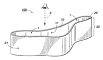
5:カーボン・ナノチューブ
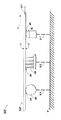
9:接地源
9.1、9.2、9.3:接地パス
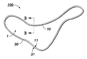
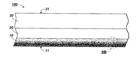
10:内側バッキング層
11:バッキング層表面
20:基層
30:外側画像形成層
31:画像形成層表面
40:バッカーバー
50:接地ブラシ
60:接地装置
100:画像形成ベルト
200:画像形成装置
Claims (5)
- 画像形成ベルトを含む画像形成装置であって、
前記画像形成ベルトが、基層と、外側の画像形成層と、1つ又はそれ以上のカーボン・ナノチューブが内部に配置された内側のバッキング層とを含む、
ことを特徴とする画像形成装置。 - 前記画像形成ベルトの前記バッキング層が、抗カール性バッキング層をさらに含むことを特徴とする請求項1に記載の画像形成装置。
- 前記画像形成ベルトの前記内側バッキング層はバッキング層表面を含み、前記画像形成装置は、1つ又はそれ以上含まれる導電性のバッカーバーにより、前記バッキング層表面を接地源に結合するように配置されることを特徴とする請求項1に記載の画像形成装置。
- 前記画像形成ベルトの前記内側バッキング層はバッキング層表面を含み、前記画像形成装置は、1つ又はそれ以上含まれる導電性の接地ブラシにより、前記バッキング層表面を接地源に結合するように配置されることを特徴とする請求項1に記載の画像形成装置。
- 前記画像形成ベルトの前記内側バッキング層はバッキング層表面を含み、前記画像形成装置は、少なくとも1つ含まれる導電性のバッカーバーを、少なくとも1つ含まれる導電性接地ブラシと併せて用いて、前記バッキング層表面を接地源に結合するように配置されることを特徴とする請求項1に記載の画像形成装置。
Applications Claiming Priority (2)
| Application Number | Priority Date | Filing Date | Title |
|---|---|---|---|
| US11/496,532 | 2006-07-31 | ||
| US11/496,532 US7851111B2 (en) | 2006-07-31 | 2006-07-31 | Imaging belt with nanotube backing layer, and image forming devices including the same |
Related Parent Applications (1)
| Application Number | Title | Priority Date | Filing Date |
|---|---|---|---|
| JP2007192068A Division JP5085217B2 (ja) | 2006-07-31 | 2007-07-24 | ナノチューブのバッキング層をもつ画像形成ベルト及びそのベルトを含む画像形成装置 |
Publications (2)
| Publication Number | Publication Date |
|---|---|
| JP2012247802A true JP2012247802A (ja) | 2012-12-13 |
| JP5350525B2 JP5350525B2 (ja) | 2013-11-27 |
Family
ID=38564038
Family Applications (2)
| Application Number | Title | Priority Date | Filing Date |
|---|---|---|---|
| JP2007192068A Expired - Fee Related JP5085217B2 (ja) | 2006-07-31 | 2007-07-24 | ナノチューブのバッキング層をもつ画像形成ベルト及びそのベルトを含む画像形成装置 |
| JP2012194682A Expired - Fee Related JP5350525B2 (ja) | 2006-07-31 | 2012-09-05 | ナノチューブのバッキング層をもつ画像形成ベルト及びそのベルトを含む画像形成装置 |
Family Applications Before (1)
| Application Number | Title | Priority Date | Filing Date |
|---|---|---|---|
| JP2007192068A Expired - Fee Related JP5085217B2 (ja) | 2006-07-31 | 2007-07-24 | ナノチューブのバッキング層をもつ画像形成ベルト及びそのベルトを含む画像形成装置 |
Country Status (4)
| Country | Link |
|---|---|
| US (1) | US7851111B2 (ja) |
| EP (1) | EP1884833B1 (ja) |
| JP (2) | JP5085217B2 (ja) |
| DE (1) | DE602007002752D1 (ja) |
Families Citing this family (3)
| Publication number | Priority date | Publication date | Assignee | Title |
|---|---|---|---|---|
| US8211601B2 (en) | 2009-04-24 | 2012-07-03 | Xerox Corporation | Coating for optically suitable and conductive anti-curl back coating layer |
| US8465893B2 (en) * | 2010-08-18 | 2013-06-18 | Xerox Corporation | Slippery and conductivity enhanced anticurl back coating |
| US8718528B2 (en) | 2012-01-17 | 2014-05-06 | Xerox Corporation | Efficient fusing and fixing for toners comprising opto-thermal elements |
Citations (9)
| Publication number | Priority date | Publication date | Assignee | Title |
|---|---|---|---|---|
| JPS61116373A (ja) * | 1984-11-10 | 1986-06-03 | Toshiba Corp | 現像剤供給装置 |
| JPH0519567A (ja) * | 1991-03-29 | 1993-01-29 | Hitachi Koki Co Ltd | 電子写真記録装置 |
| JPH0566704A (ja) * | 1991-09-09 | 1993-03-19 | Hitachi Ltd | ベルト状感光体 |
| JPH0525466U (ja) * | 1991-03-01 | 1993-04-02 | 富士ゼロツクス株式会社 | 電子写真複写機等の画像形成装置 |
| JPH09138518A (ja) * | 1995-11-16 | 1997-05-27 | Konica Corp | 電子写真感光体、画像形成方法及び装置 |
| JP2003215828A (ja) * | 2001-10-09 | 2003-07-30 | Xerox Corp | 応力除去方法 |
| JP2004185983A (ja) * | 2002-12-03 | 2004-07-02 | Toyobo Co Ltd | 導電性樹脂組成物 |
| JP2006084987A (ja) * | 2004-09-17 | 2006-03-30 | Fuji Denki Gazo Device Kk | 電子写真用感光体 |
| JP2006517485A (ja) * | 2003-01-30 | 2006-07-27 | タキロン株式会社 | 分散した導電層を有する成形体 |
Family Cites Families (14)
| Publication number | Priority date | Publication date | Assignee | Title |
|---|---|---|---|---|
| US4402593A (en) * | 1981-12-31 | 1983-09-06 | Pittney Bowes Inc. | Grounding device for moving photoconductor web |
| JPH0624848Y2 (ja) * | 1984-12-29 | 1994-06-29 | 株式会社リコー | 複写装置 |
| US4654284A (en) * | 1985-10-24 | 1987-03-31 | Xerox Corporation | Electrostatographic imaging member with anti-curl layer comprising a reaction product of a binder bi-functional coupling agent and crystalline particles |
| US5008167A (en) * | 1989-12-15 | 1991-04-16 | Xerox Corporation | Internal metal oxide filled materials for electrophotographic devices |
| US5021309A (en) * | 1990-04-30 | 1991-06-04 | Xerox Corporation | Multilayered photoreceptor with anti-curl containing particulate organic filler |
| US5167987A (en) * | 1991-11-04 | 1992-12-01 | Xerox Corporation | Process for fabricating electrostatographic imaging members |
| US5215841A (en) * | 1991-12-30 | 1993-06-01 | Xerox Corporation | Electrophotographic imaging member with overcoatings containing fullerenes |
| US5382486A (en) * | 1993-03-29 | 1995-01-17 | Xerox Corporation | Electrostatographic imaging member containing conductive polymer layers |
| US6101353A (en) * | 1998-12-21 | 2000-08-08 | Xerox Corporation | Flexible photoreceptor belt detensioning for charge transport layer cracking life extension |
| US6303254B1 (en) * | 2000-10-20 | 2001-10-16 | Xerox Corporation | Electrostatographic imaging member |
| KR20040030553A (ko) * | 2001-03-26 | 2004-04-09 | 에이코스 인코포레이티드 | 탄소 나노튜브를 함유하는 코팅막 |
| US6766128B2 (en) * | 2002-11-12 | 2004-07-20 | Xerox Corporation | Precision partially cylindrical web guide member and improved manufacturing process for making the same |
| US6751429B1 (en) * | 2002-12-16 | 2004-06-15 | Xerox Corporation | Compliant backer bar |
| JP2006030528A (ja) | 2004-07-15 | 2006-02-02 | Oki Data Corp | 無端状ベルト搬送体および画像形成装置 |
-
2006
- 2006-07-31 US US11/496,532 patent/US7851111B2/en not_active Expired - Fee Related
-
2007
- 2007-07-19 EP EP07112732A patent/EP1884833B1/en not_active Ceased
- 2007-07-19 DE DE602007002752T patent/DE602007002752D1/de active Active
- 2007-07-24 JP JP2007192068A patent/JP5085217B2/ja not_active Expired - Fee Related
-
2012
- 2012-09-05 JP JP2012194682A patent/JP5350525B2/ja not_active Expired - Fee Related
Patent Citations (9)
| Publication number | Priority date | Publication date | Assignee | Title |
|---|---|---|---|---|
| JPS61116373A (ja) * | 1984-11-10 | 1986-06-03 | Toshiba Corp | 現像剤供給装置 |
| JPH0525466U (ja) * | 1991-03-01 | 1993-04-02 | 富士ゼロツクス株式会社 | 電子写真複写機等の画像形成装置 |
| JPH0519567A (ja) * | 1991-03-29 | 1993-01-29 | Hitachi Koki Co Ltd | 電子写真記録装置 |
| JPH0566704A (ja) * | 1991-09-09 | 1993-03-19 | Hitachi Ltd | ベルト状感光体 |
| JPH09138518A (ja) * | 1995-11-16 | 1997-05-27 | Konica Corp | 電子写真感光体、画像形成方法及び装置 |
| JP2003215828A (ja) * | 2001-10-09 | 2003-07-30 | Xerox Corp | 応力除去方法 |
| JP2004185983A (ja) * | 2002-12-03 | 2004-07-02 | Toyobo Co Ltd | 導電性樹脂組成物 |
| JP2006517485A (ja) * | 2003-01-30 | 2006-07-27 | タキロン株式会社 | 分散した導電層を有する成形体 |
| JP2006084987A (ja) * | 2004-09-17 | 2006-03-30 | Fuji Denki Gazo Device Kk | 電子写真用感光体 |
Also Published As
| Publication number | Publication date |
|---|---|
| DE602007002752D1 (de) | 2009-11-26 |
| EP1884833B1 (en) | 2009-10-14 |
| US20080026309A1 (en) | 2008-01-31 |
| JP2008033321A (ja) | 2008-02-14 |
| JP5085217B2 (ja) | 2012-11-28 |
| JP5350525B2 (ja) | 2013-11-27 |
| US7851111B2 (en) | 2010-12-14 |
| EP1884833A1 (en) | 2008-02-06 |
Similar Documents
| Publication | Publication Date | Title |
|---|---|---|
| US8290418B2 (en) | Heating member using carbon nanotube and fixing unit using the heating member | |
| CA2594113C (en) | Carbon nanotube composites for blade cleaning in electrophotographic marking systems | |
| US9441131B2 (en) | CNT/fluoropolymer coating composition | |
| US10133204B2 (en) | Imaging device components comprised of hydrophobic carbon nanotubes | |
| US8557345B2 (en) | Process for making CNT/PFA composite coatings for fuser applications | |
| US8859667B2 (en) | Carbon nanotube filled polycarbonate anti-curl back coating with improved electrical and mechanical properties | |
| JP5350525B2 (ja) | ナノチューブのバッキング層をもつ画像形成ベルト及びそのベルトを含む画像形成装置 | |
| CA2690278C (en) | Fluorinated carbon nanotubes and teflon related nanocomposites | |
| JP2011089120A (ja) | マーキングサブシステム用途のためのハイパーナノコンポジット(hnc)からなる機能性表面 | |
| US7228091B2 (en) | Compact charging method and device with gas ions produced by electric field electron emission and ionization from nanotubes | |
| JP2011022575A (ja) | 誘導加熱式カーボンナノチューブ定着器 | |
| JP5306622B2 (ja) | 光学的に透明な導電性のエレクトロルミネセンス・カーボンナノチューブ接地面を有する自己消去型感光体 | |
| US8962736B2 (en) | Electrically resistive coatings/layers using soluble carbon nanotube complexes in polymers | |
| JP3778724B2 (ja) | 接触型帯電器及び画像記録装置 | |
| JP2014016611A (ja) | 定着器システム | |
| JP2004279917A (ja) | 画像形成装置用導電性部品及び画像形成装置 | |
| JP3306310B2 (ja) | 画像形成装置 | |
| JP2005316395A (ja) | 画像形成装置 | |
| JPH0643776A (ja) | 定着装置 | |
| US10591856B2 (en) | Roller with filler bundle in elastic layer and fixing device | |
| JP6264039B2 (ja) | 導電性シートの製造方法 | |
| JP4155484B2 (ja) | 接触型帯電器および画像形成装置 | |
| JP2004279916A (ja) | 現像装置及び画像形成装置 | |
| JP4891681B2 (ja) | 画像形成装置用ロールブラシ | |
| JP6278018B2 (ja) | 帯電装置及び画像形成装置 |
Legal Events
| Date | Code | Title | Description |
|---|---|---|---|
| A521 | Request for written amendment filed |
Free format text: JAPANESE INTERMEDIATE CODE: A523 Effective date: 20120906 |
|
| A621 | Written request for application examination |
Free format text: JAPANESE INTERMEDIATE CODE: A621 Effective date: 20120906 |
|
| TRDD | Decision of grant or rejection written | ||
| A01 | Written decision to grant a patent or to grant a registration (utility model) |
Free format text: JAPANESE INTERMEDIATE CODE: A01 Effective date: 20130722 |
|
| A61 | First payment of annual fees (during grant procedure) |
Free format text: JAPANESE INTERMEDIATE CODE: A61 Effective date: 20130821 |
|
| R150 | Certificate of patent or registration of utility model |
Ref document number: 5350525 Country of ref document: JP Free format text: JAPANESE INTERMEDIATE CODE: R150 Free format text: JAPANESE INTERMEDIATE CODE: R150 |
|
| R250 | Receipt of annual fees |
Free format text: JAPANESE INTERMEDIATE CODE: R250 |
|
| R250 | Receipt of annual fees |
Free format text: JAPANESE INTERMEDIATE CODE: R250 |
|
| R250 | Receipt of annual fees |
Free format text: JAPANESE INTERMEDIATE CODE: R250 |
|
| R250 | Receipt of annual fees |
Free format text: JAPANESE INTERMEDIATE CODE: R250 |
|
| R250 | Receipt of annual fees |
Free format text: JAPANESE INTERMEDIATE CODE: R250 |
|
| LAPS | Cancellation because of no payment of annual fees |