JP2012248657A - Die bonder and die bonding method - Google Patents
Die bonder and die bonding method Download PDFInfo
- Publication number
- JP2012248657A JP2012248657A JP2011118851A JP2011118851A JP2012248657A JP 2012248657 A JP2012248657 A JP 2012248657A JP 2011118851 A JP2011118851 A JP 2011118851A JP 2011118851 A JP2011118851 A JP 2011118851A JP 2012248657 A JP2012248657 A JP 2012248657A
- Authority
- JP
- Japan
- Prior art keywords
- die
- bonding
- unit
- stage
- prestage
- Prior art date
- Legal status (The legal status is an assumption and is not a legal conclusion. Google has not performed a legal analysis and makes no representation as to the accuracy of the status listed.)
- Withdrawn
Links
Images



Landscapes
- Die Bonding (AREA)
Abstract
【課題】小型ダイボンダを並びにスループット低下を低減できるダイボンダ及びボンディング方法を提供する。
【解決手段】ダイ供給部に保持されたウェハからダイをピックアップし、プリアライメントステージ31sに前記ダイを載置し、前記プリアライメントステージから前記ダイをボンディングヘッド41pがピックアップし、前記ダイ供給部の上面より上側に設けられた部品認識カメラ42によって前記ボンディングヘッド41pでピックアップした前記ダイの保持状態を撮像し、前記撮像ステップの撮像結果に基づいて前記ボンディング位置・姿勢を補正して基板にボンディングすることを第1の特徴とする。また、プリアライメントステージ31sに前記ダイを載置する載置位置は、前記基板へのボンディング位置及び前記部品認識カメラ42の先端面の同じかほぼ同一レベルより相対的に下げ、ダイ供給部の上面より上側に設けることを第2の特徴とする。
【選択図】図4A small die bonder and a die bonder and a bonding method capable of reducing a decrease in throughput are provided.
A die is picked up from a wafer held in a die supply unit, the die is placed on a pre-alignment stage 31s, and the bonding head 41p picks up the die from the pre-alignment stage. An image of the holding state of the die picked up by the bonding head 41p is picked up by a component recognition camera 42 provided above the upper surface, and the bonding position / orientation is corrected based on the image pickup result of the image pickup step and bonded to the substrate. This is the first feature. Also, the mounting position for mounting the die on the pre-alignment stage 31s is relatively lowered from the same or substantially the same level of the bonding position to the substrate and the front end surface of the component recognition camera 42, and the upper surface of the die supply unit The second feature is that it is provided on the upper side.
[Selection] Figure 4
Description
本発明は、ダイボンダ及びボンディング方法に係わり、スループット低下を低減できるダイボンダ及びボンディング方法に関する。 The present invention relates to a die bonder and a bonding method, and more particularly to a die bonder and a bonding method that can reduce a decrease in throughput.
ダイ(半導体チップ)を配線基板やリードフレームなどの基板に搭載してパッケージを組み立てる工程の一部に、ウェハからダイをピックアップ(吸着)し基板にボンディングするダイボンディング工程がある。
ダイボンディング工程を行う方法として、ピックアップしたダイを一度プリアライメントステージ(第1の作業ステージ)に載置し、ボンディングヘッドでプリアライメントステージから再度ダイをピックアップし、第2の作業ステージの搬送されてきた基板にボンディング(装着)する方法(特許文献1)がある。また、ウェハからダイをピックアップ(吸着)したダイの保持状態を部品認識カメラで撮像し、その撮像結果に基づいてボンディング位置・姿勢を補正してボンディングする方法(特許文献2)がある。
Part of the process of assembling a package by mounting a die (semiconductor chip) on a substrate such as a wiring board or a lead frame includes a die bonding process of picking up (sucking) the die from the wafer and bonding it to the substrate.
As a method of performing the die bonding process, the picked-up die is once placed on the pre-alignment stage (first work stage), the die is picked up again from the pre-alignment stage by the bonding head, and the second work stage is conveyed. There is a method (Patent Document 1) for bonding (attaching) to a substrate. In addition, there is a method (Patent Document 2) in which a holding state of a die obtained by picking up (sucking) a die from a wafer is imaged by a component recognition camera, and bonding positions and postures are corrected based on the imaging result.
しかしながら、ウェハを保持しているウェハ供給台を備えたダイ供給部が部品認識カメラと干渉しないように部品認識カメラの外側にダイ供給部を設ける必要がある。特に、ダイ供給部が複数の種類のダイを供給するために複数のウェハを有する場合に、ウェハを移動する必要がある。その場合、それぞれのウェハを保持しているウェハ保持台が部品認識カメラと干渉しないように設けるために、ダイ供給部の設置領域が広くなり、装置として寸法が大きくなってしまう。装置が大きくなると、ダイをピックアップし基板にボンディング(装着)する間の移動距離が長くなり、ボンディングサイクル時間が長くなり、スループットが低下する課題がある。上記、特許文献1、2は上記の課題を認識しておらず、当然その課題に対する解決する手段の開示も示唆もない。
However, it is necessary to provide the die supply unit outside the component recognition camera so that the die supply unit including the wafer supply table holding the wafer does not interfere with the component recognition camera. In particular, when the die supply unit has a plurality of wafers to supply a plurality of types of dies, it is necessary to move the wafers. In that case, since the wafer holding table holding each wafer is provided so as not to interfere with the component recognition camera, the installation area of the die supply unit is widened, and the size of the apparatus is increased. As the apparatus becomes larger, there is a problem that the moving distance between picking up the die and bonding (mounting) to the substrate becomes longer, the bonding cycle time becomes longer, and the throughput decreases. The above-mentioned
従って、本発明の第1目的は、小型ダイボンダを提供することである。
また、本発明の第1目的は、スループット低下を低減できるダイボンダ及びボンディング方法を提供することである。
Accordingly, a first object of the present invention is to provide a small die bonder.
In addition, a first object of the present invention is to provide a die bonder and a bonding method that can reduce a decrease in throughput.
本発明は、上記目的を達成するために、少なくとも以下の特徴を有する。
本発明は、ダイ供給部に保持されたウェハからダイをピックアップし、プリアライメントステージに前記ダイを載置し、ボンディングヘッドが前記プリアライメントステージから前記ダイをピックアップし、前記ダイ供給部の上面より上側に設けられた部品認識カメラによって前記ボンディングヘッドでピックアップした前記ダイの保持状態を撮像し、前記撮像ステップの撮像結果に基づいて前記ボンディング位置・姿勢を補正して基板にボンディングすることを第1の特徴とする。
In order to achieve the above object, the present invention has at least the following features.
The present invention picks up a die from a wafer held in a die supply unit, places the die on a pre-alignment stage, and a bonding head picks up the die from the pre-alignment stage. First, imaging a holding state of the die picked up by the bonding head with a component recognition camera provided on the upper side, correcting the bonding position / orientation based on an imaging result of the imaging step, and bonding to the substrate It is characterized by.
また、本発明は、プリアライメントステージに前記ダイを載置する載置位置は、前記基板へのボンディング位置及び前記部品認識カメラの先端面と同じかほぼ同一レベルより相対的に下げ、前記ウェハの上面より上側に設けることを第2の特徴とする。 Further, the present invention provides that the mounting position for mounting the die on the pre-alignment stage is relatively lower than the bonding position on the substrate and the front end surface of the component recognition camera, or relatively lower than the same level. A second feature is that the upper surface is provided above the upper surface.
さらに、前記ボンディングヘッドが前記ダイをピックアップする受渡位置に前記プリアライメントステージを移動させることを第3の特徴とする。
また、本発明は、前記プリステージの移動は、前記プリアライメントステージの昇降、前記部品認識カメラ側への水平移動のうち少なくとも一方を有することを第4の特徴とする。
Furthermore, a third feature is that the pre-alignment stage is moved to a delivery position where the bonding head picks up the die.
According to a fourth aspect of the present invention, the movement of the prestage includes at least one of raising / lowering of the prealignment stage and horizontal movement toward the component recognition camera.
さらに、本発明は、前記プリステージの移動は、前記プリステージ昇り移動と、前記プリステージの前記部品認識カメラ側への水平移動とを並行して行うことを第5の特徴とする。
また、本発明は、前記ボンディングヘッドが前記ダイをピックアップする受渡位置に近接し、その後前記プリアライメントステージから前記ダイをボンディングヘッドがピックアップすることを第6の特徴とする。
The fifth aspect of the present invention is that the movement of the prestage is performed in parallel with the movement of the prestage rising and the horizontal movement of the prestage toward the component recognition camera.
Further, the present invention is characterized in that the bonding head is close to a delivery position for picking up the die, and then the bonding head picks up the die from the pre-alignment stage.
さらに、本発明は、前記ダイ供給部は、複数の前記ウェハと、複数の前記ウェハを保持するウェハ保持ステージとを有し、前記ウェハ保持ステージを前記垂直な面内で回転させることを第7の特徴とする。
また、本発明は、複数の前記ウェハのダイのピックアップ位置を移動させることを第8の特徴とする。
Further, according to the present invention, the die supply unit includes a plurality of the wafers and a wafer holding stage for holding the plurality of wafers, and is configured to rotate the wafer holding stage in the vertical plane. It is characterized by.
The eighth feature of the present invention is that the pick-up positions of a plurality of wafer dies are moved.
従って、本発明によれば、ダイ供給部のウェハ保持台と部品認識カメラとの干渉を避けるように、ダイ供給部を部品認識カメラの設置位置より下部に設けることで小型なダイボンダを提供できる。
また、本発明よれば、プリアライメントステージとボンディンヘッドとを協調して受渡位置に移動させることでスループット低下を低減できるダイボンダ及びボンディング方法を提供できる。
Therefore, according to the present invention, a small die bonder can be provided by providing the die supply unit below the installation position of the component recognition camera so as to avoid interference between the wafer holder of the die supply unit and the component recognition camera.
Further, according to the present invention, it is possible to provide a die bonder and a bonding method that can reduce a decrease in throughput by cooperatively moving the pre-alignment stage and the bonding head to the delivery position.
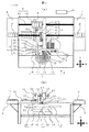
図1は本発明の実施形態であるダイボンダ100の概略図を示す図である。図1(a)は、ダイボンダ100の上面図であり、図1(b)は図1(a)において矢印Aから見た正面図である。
ダイボンダ100は、大別して、複数のウェハ11(図1では4枚)を保持する4つのウェハ保持台12とウェハ11からダイDを突き上げる点線で示す突き上げユニット13とを有するダイ供給部1と、突き上げユニット13で突き上げられたダイDを吸着してピックアップし、プリアライメントステージ(以下、単にプリステージという)31に載置するピックアップ部2と、プリステージ31を有し、ダイDを複数個載置(図示せず)したプリステージ31を図1(a)に示すX、Y方向及び図1(b)に示すZ方向に移動させるプリアライメント部3と、プリステージ31上のダイDをボンディングヘッド41でピックアップし、ボンディングヘッド41のダイDの保持状態を部品認識カメラ42で撮像し、その撮像結果に基づいてボンディング位置・姿勢を補正して搬送されてきた基板Pにボンディングするボンディング部4と、複数(4)枚の基板Pを搬送する基板搬送パレット51に基板を供給する基板供給部6、基板搬送パレット51を基板供給部6からボンディング位置を経由して基板搬出部7まで搬送する搬送部5と、ダイDがボンディング(装着)された基板Pを基板搬送パレット51から受け取り基板搬出部7と、各部の動作を監視し制御する制御部8と、を有する。
FIG. 1 is a diagram showing a schematic view of a
The die
次に、実施形態のダイボンダ100の各部の構成と動作を図1を主体により詳細に説明する。
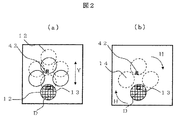
まず、ダイ供給部1を説明する。図2は、ウェハ保持台12の動作を模式的に示す図である。ウェハ保持台12はウェハ保持ステージ14(図1(a)参照)の4辺側に固定されている。ウェハ保持ステージ14は、図1(b)に示す保持部基台17に設けられたXY駆動部15により図2(a)に示すY方向の移動例のようにX、Y方向に移動し、さらにXY駆動部15上に設けられた回転駆動部16により図2(b)示すよう回転可能に設けられている。一方、突き上げユニット13は、保持部基台17の所定位置に基本的には固定され、その位置に存在するウェハ11のダイDを突き上げる。基本的とは、微調整機構を有することもあることを示す。
Next, the configuration and operation of each part of the
First, the die
上記の構成のうち回転駆動部16によってウェハ11(ウェハ保持台12)を選択し、XY駆動部15によって選択されたウェハ上の所定位置のダイDを突き上げユニット13の上部に移動させる。本実施形態では4枚のウェハから1個ずつダイをピックアップするから、まず、ピックアップされるダイの位置、即ちダイ供給部1をピックアップヘッド21に垂直な面内で移動させるXY駆動部(2方向移動手段)15で決め、その後90度ずつウェハ保持台12を順次回転させて4枚のウェハからダイDを順次ピックアップする。この場合、回転したときにピックアップ位置においてダイDが同一姿勢になうように各ウェハをウェハ保持台に載置することが望ましい。次に、隣接するダイをピックアップできるようにウェハ保持ステージ14をXY駆動部15で移動する。その後、これ等動作を繰り返して行う。
上記実施形態では、ダイのピックアップ位置をXY駆動部15で決めたが、XY方向に突き上げユニット13を移動させる突き上げユニット移動手段を設けて突き上げユニット13を移動させてもよい。
The wafer 11 (wafer holder 12) is selected by the
In the above embodiment, the pick-up position of the die is determined by the
次に、ピックアップ部2は、突き上げユニット13で突き上がられたダイを吸着してピックアップするピックアップヘッド21と、ピックアップヘッド21をX方向に移動させるX駆動軸22と、ウェハ11のアライメントマーク(図示せず)を撮像し、ピックアップすべきダイDの位置を認識するウェハ認識カメラ23(図1(b)参照)とを、有する。X駆動軸22によってピックアップヘッド21は、ダイDの突き上げ位置とプリステージ31間を往復し、4個のダイをプリステージ31にプリステージの長手(Y)方向に列状に配置する。
Next, the
次に、プリアライメント部3を説明する前にボンディング部4等を説明する。ボンディング部4は、プリステージ31からダイDをピックアップし、搬送されてきた基板Pにボンディングするボンディングヘッド41、ボンディングヘッド41のダイDの保持状態を撮像する部品認識カメラ42と、ボンディングヘッド41をY方向に移動させるY駆動軸43と、搬送されていた基板Pの位置認識マーク(図示せず)を撮像し、ボンディングすべきダイDのボンディング位置を認識する基板認識カメラ44と、を有する。ボンディングヘッド41はY駆動軸43のほか、先端に複数設けられた吸着ノズル41aを昇降する図示しないヘッド昇降手段を有する。
Next, the
このような構成によって、ボンディングヘッド41は、プリステージ31からダイDをピックアップし、Y駆動軸に沿って移動中に部品認識カメラ42でダイDの保持状態を撮像し、その結果に基づいてボンディング位置・姿勢を補正して、基板PにダイDをボンディングする。この動作をプリステージ31上の4個のダイに対して同時に又は個別に行なう。
With such a configuration, the
搬送部5は、一枚又は複数枚の基板(図1では4枚)を載置した基板搬送パレット51と、基板搬送パレット51が移動するパレットレール52とを具備する同一構造の第1、第2搬送部とが並行して設けられている。基板搬送パレット51は、基板搬送パレットに設けられた図示しないナットをパレットレール52に沿って設けられた図示しないボールネジで駆動することによって移動する。
The
このような構成によって、基板搬送パレット51は、基板供給部6で基板を載置され、パレットレール52に沿ってボンディング位置まで移動し、ボンディング後基板搬出部7まで移動して基板搬出部7に基板を渡す。第1、第2搬送部は、互いに独立して駆動され、一方の基板搬送パレット51に載置された基板PにダイDをボンディング中に、他方の基板搬送パレット51は、基板Pを搬出し、基板供給部6に戻り、新たな基板を載置するなどの準備を行なう。
With such a configuration, the
なお、本実施形態のダイボンダにおいて、直線的に移動させる駆動機構にもボールネジ/ナット方式など採用している。また、搬送部等の駆動機構としては、上記のボールネジ/ナット方式に限らず、リニアモータ方式を用いてもよい。 In the die bonder of this embodiment, a ball screw / nut system or the like is also used for the drive mechanism that moves linearly. Further, the drive mechanism such as the conveying unit is not limited to the above-described ball screw / nut method, and a linear motor method may be used.
最後に、本発明の課題と共に、本課題を解決するプリアライメント部3の構成と動作を説明する。
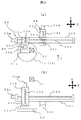
まず、本発明の課題とプリアライメント部3の動作を図2及び図3を用いて説明する。図3は、図2(a)に示す4台のウェハ保持台12(ウェハ11)のうち格子状に示したウェハ11を有するウェハ保持台12と部品認識カメラ42とのY方向における関係を示す図である。ウェハ保持台12(ウェハ11)は、図2を用いて既に説明したようにX、Y方向に移動する。
Finally, the configuration and operation of the
First, the problem of the present invention and the operation of the
従来では、図3(c)に示すように、ボンディングヘッド41は、ダイDのピックアップ・ボンディングに必要な最低限の上下移動し、プリステージ31と基板Pとの間を矢印Gに示すように水平往復移動していた。そのために、部品認識カメラ42は、ボンディングヘッド41にピックアップされているダイDの保持状態を監視するために、プリステージ31と基板Pより下のウェハ保持台12と同じかほぼ同一レベルになるように配置していた。ほぼ同一レベルとは、ボンディングヘッド41の水平往復移動に差し支えないようにその移動レベルに近接した位置をいう。
Conventionally, as shown in FIG. 3 (c), the
一方、図3(a)、図3(b)示す本実施形態では、第1に、ダイ供給部1の小型化を図るために、部品認識カメラ42を前記ダイ供給部と干渉しないように前記ダイ供給部の上面より上側の高い位置に設置する。その結果、4台のウェハ保持台12が互いに隣接する位置まで最大狭くすることができる。例えば、部品認識カメラ42を4台のウェハ保持台12の中心位置の上部に配置した時の1台のウェハ保持台12による効果が図3に示すようにΔαであるとすれば、この1台のウェハ保持台12に対向したウェハ保持台12による効果も同様にΔαであり、この結果、ダイ供給部1のX、Y方向の幅をそれぞれ2Δα小さくできる。その他の構成部の兼ね合いがあるので必ずしも2Δα分小さくできると限らないが、少なくとも図2(a)に示す格子状の位置のY方向のΔαの効果は奏する。
On the other hand, in the present embodiment shown in FIGS. 3A and 3B, first, in order to reduce the size of the
以上の説明では、ウェハ保持台12(ウェハ11)を4台設ける場合を説明したが、1台でも、さらに、2台、3台又は5台以上でも同様な手段で同様な効果を奏することができる。
また、ダイ供給部1を有したダイボンダの小型化の結果、ダイDをウェハ11からピックアップし基板Pへのボンディングする間の処理時間の短縮をできる。
In the above description, the case where four wafer holding tables 12 (wafers 11) are provided has been described, but the same effect can be obtained with the same means with one, two, three, or five or more. it can.
Further, as a result of miniaturization of the die bonder having the
処理時間を短縮するために、第2に、ピックアップ部2による載置時のプリステージ31の載置位置31sを設定する。第1の方法は、図3(a)に示すように、ボンディングヘッド41と部品認識カメラ42及び基板Pとの位置関係を従来技術と同様にし、言い換えれば、前記基板へのボンディング位置及び前記部品認識カメラの先端面の位置は同じかほぼ同一レベルにし、ピックアップ部2による載置時のプリステージ31の位置を前記2つの位置に対して相対的に下げ、ダイ供給部1の上面より上側に設ける。第2の方法は、図3(b)に示すように、プリステージ31の載置位置31sを前記基板へのボンディング位置及び前記部品認識カメラの先端面の位置と同じかほぼ同一レベルにする方法である。第3の方法は、プリステージ31の載置位置31sを第1の方法と第2の方法の中間位置に設ける方法である。第2及び第3では、ピックアップヘッド21の動作範囲を広くする必要がある。
Secondly, in order to shorten the processing time, a
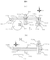
処理時間を短縮するために、第3に、ダイDをウェハ11からピックアップし基板Pへのボンディングする間の処理時間をプリステージ31及びボンディング41に分担させて、処理時間を短縮する。図4は、第1の方法を主体に示したプリステージ31とボンディングヘッド41の移動パターンを示す。
Thirdly, in order to shorten the processing time, the processing time is reduced by sharing the processing time during which the die D is picked up from the
次に、図4を用いて具体的にプリステージ31とボンディングヘッド41の動作を上記第1の方法を主体に説明する。図4において、実線または二点鎖線はプリステージ31を、破線はボンディングヘッド41を示す。また、プリステージ31の添え字sは、前述したようにピックアップヘッド21による載置位置31sを示す。同じく添え字pはボンディングヘッド41によるピックアップ位置である受渡位置を示し、同じく添え字cは載置位置31sから受渡位置へ31pの中継位置を示す。また、ボンディングヘッド41の添え字pは、プリステージ31からの受渡位置を示し、同じく添え字cは受渡位置41pから基板Pへの中継位置を示す。図4(a)から図4(f)に示すように、ボンディングヘッド41がダイDをピックアップするプリステージ31の受渡位置31pは、ボンディングヘッド41がダイDの保持状態を撮像する必要があるために、部品認識カメラ42よりピックアップ位置側にあるという条件を満たす必要がある。
Next, the operations of the
図4(a)から図4(c)は、上記第1の方法の典型的な例を示し、ピックアップヘッド21がプリステージ31にダイDを搭載する処理時間が、ボンディングヘッド41がダイDをピックアップし基板Pにボンディングする処理時間より大幅に短い場合に適した例である。この場合は、プリステージ31が部品認識カメラ42側に水平方向に移動すると共に、ボンディングヘッド41の水平移動レベルまで上昇する。図4(a)は、プリステージ31が部品認識カメラ42側に水平に移動し、その後ボンディングヘッド41の水平移動レベルに上昇するパターンを示す。図4(b)は、逆にプリステージ31がボンディングヘッド41の水平移動レベルに上昇し、その後部品認識カメラ42側に水平に移動するパターンを示す。図4(c)は、プリステージ31がボンディングヘッド41の水平移動レベルに上昇しながら部品認識カメラ42側に水平に移動するパターンを示す。また図4(a)から図4(c)において、例えばプリステージ31が移動する間にボンディングヘッドも移動する。
4 (a) to 4 (c) show a typical example of the first method, in which the processing time for the
図4(d)から図4(e)は、ピックアップヘッド21がプリステージ31にダイDを搭載する処理時間とボンディングヘッド41がダイDをピックアップし基板Pにボンディングする処理時間とが拮抗する場合の示す例である。この場合は、ボンディングヘッド41もプリステージ31と共に、受渡位置41pに向けて移動する。図4(d)は、プリステージ31がボンディングヘッド41の水平移動レベル上昇し、その上昇した載置位置31pにボンディングヘッド41がさらに水平移動するパターンである。図4(d)において、ピックアップヘッドの昇降範囲を広くすることで受渡位置31pを載置位置31sとすれば上述した第2の方法となる。
4D to 4E show the case where the processing time for the
図4(e)は、プリステージ31とボンディングヘッド41共に、図4(c)のように水平に移動しながら上昇或いは下降するパターンである。図4(e)は、図4(d)と同様に受渡位置31pを載置位置31sすれば上述した第3の方法となる。
FIG. 4E shows a pattern in which both the
図4(f)は、図4(a)から図4(c)とは異なり、ボンディングヘッド41がダイDをピックアップし基板Pにボンディングする処理時間が、ピックアップヘッド21がプリステージ31にダイDを搭載する処理時間より短い場合を示す例である。この場合は、図4(a)から図4(c)に示したプリステージ31の移動とは異なりボンディングヘッド41が移動するパターンが考えられる。図4(f)は、その例として図4(c)に対応してボンディングヘッド41が移動するパターンを示す。即ち、プリステージ31が移動せず、ボンディングヘッド41がプリステージ31側に水平に移動しながら、プリステージ31の上部のレベルまで下降するパターンを示す。
4 (f) is different from FIGS. 4 (a) to 4 (c) in that the processing time for the
図4(e)、図4(f)においては、ボンディングヘッド4部は、ボンディングヘッド41がプリステージ31からダイDをピックアップし基板Pにボンディングするのに必要な昇降ストロークに、さらにプリステージ31の受渡位置31sに近接するのに必要なストロークを有する昇降手段が必要である。
4 (e) and 4 (f), the
次に、図1に戻って、図4(a)から図4(e)に示すプリアライメント部3の構成を説明する。プリアライメント部3は、ピックアップ21によりピックアップされたダイDを載置するプリステージ31と、プリステージ31を昇降させるZ駆動軸(プリステージ昇降手段)32と、Z駆動軸32を水平である図1(a)の紙面上下(Y)方向に移動させるY駆動軸(プリステージ水平移動手段)33と、Y駆動軸33を図1(a)の紙面左右(X)方向に移動させるX駆動軸34と、ダイDのプリステージ31への載置状態を撮像する載置部品認識カメラ35と、を有する。
Next, returning to FIG. 1, the configuration of the
図5、図6は、プリアライメント部3の詳細構成を示す図である。図5は、プリアライメント部3がウェハ11からダイDをピックアップした後、プリステージ31に載置する状態を示す図である。図6は、各ウェハ保持台12のウェハ11からダイDがそれぞれプリステージ31に載置された後、プリステージ31が、例えば図4(c)に示す移動ルートを経て、ボンディングヘッド41との受渡位置31pに移動した状態を示す図である。図5(a)、図6(a)はプリアライメント部3の上面図を示し、図5(b)、図6(b)は、それぞれ図5(a)、図6(a)に示す矢印Jの方向から見た側面図を示す。
5 and 6 are diagrams illustrating a detailed configuration of the
本実施形態のZ駆動軸32、Y駆動軸33及びX駆動軸34は、基本的に同一構成を有する。各軸は、それぞれ各符号に、添え字mで示す駆動モータと、駆動モータで駆動される添え字bで示すボールネジと、ボールネジ上を移動する添え字nで示すナットと、ナットを含有し被駆動体に連結される添え字sで示す連結体と、連結体の摺動走行路となる添え字dで示す走行基台とを有する。但し、X駆動軸34の走行基台34dはダイボンダ100の構成部材に固定され、Z駆動軸32は連結体を設けずナット32nが被駆動体である直接プリステージ31に連結されている。
The
これらの3つの駆動軸のうちZ駆動軸32は、ボールネジ32bによって移動するナット32nに固定された被駆動体であるプリステージ31を走行基台32dに沿って軸方向に昇降させる。Y駆動軸33は、プリステージ31を保持したZ駆動軸33全体を被駆動体とし、ボールネジ33bによって走行基台32dに固定され、ナット33nを内部に有する連結体33sを走行基台33dに沿ってY方向に移動させる。さらに、X駆動軸34は、プリステージ31、Z駆動軸33を保持したY駆動軸33全体を被駆動体とし、ボールネジ34bによって走行基台33dに固定され、ナット34nを内部に有する連結体34sを走行基台34dに沿ってX方向に移動させる。なお、X駆動軸33は必ずしも必要ではないが、初期設定時の微調整や、構成上必要な場合に有用である。
Of these three drive shafts, the
図5、図6に示したプリアライメント部3の駆動部によって、図4の図4(a)から図4(e)に示すプリステージ31の動きを実現できる。
The movement of the
一方、図4の図4(d)から図4(f)に示すボンディングヘッド41の動きは、ボンディングヘッド41のY方向、Z方向の動作範囲をそれぞれ又は両方を広くすることで実現できる。
On the other hand, the movement of the
最後に、以上説明した本実施形態の処理フローを図4(c)の例を基に図7を用いて説明する。
まず、XY駆動部15、回転駆動部16の少なくとも一方を制御して、所定のダイDが突き上げユニット13の位置にくるようにウェハ保持ステージ14を初期位置に設定する(ステップ1(以下S1と表記。以下同様))。次に、ピックアップ部2によってウェハ11からダイDをピックアップし、プリステージ31に載置する(S2)。そして、S2の処理を4台(全て)のウェハ保持台の12のウェハ11に対して実施したかを判断する(S3)。実施していなければ、回転駆動部16を制御してウェハ保持ステージ14を90度回転させて、S2に行く。
Finally, the processing flow of the present embodiment described above will be described with reference to FIG. 7 based on the example of FIG.
First, at least one of the
実施していれば、次の3つ処理を行う。ダイ供給部1では、次に隣接したダイDがピックアップされるようにウェハ保持ステージ14をXY移動し(S5)、S11に行く。プリアライメント部3では、プリステージ31を、例としてY駆動軸33及びZ駆動軸32を共に制御しながら図4(c)に示す曲線を描きながら受渡位置31pに移動する(S6)。ボンディング部4では、ボンディングヘッド41を受渡位置41pに移動する(S7)。
If so, the following three processes are performed. In the
次に、ボンディングヘッド41により4つのダイDをピックアップする(S8)。その後、ボンディングヘッド41はボンディング位置に移動し、搬送部5により搬送されてきた基板Pに4つのダイDをボンディングする(S9)。一方、プリステージ31はS8後、載置位置に移動する(S10)。S11では、所定のダイD又は基板Pに対して実施したかを判断し、実施していなければS2に戻り、実施していれば処理を終了する。
Next, four dies D are picked up by the bonding head 41 (S8). Thereafter, the
以上の処理フローにおいて分かり易くプリステージ31とボンディングヘッド41の動きを示したが実際はより複雑である。基本的には、プリステージ31とボンディングヘッド41とが同一の処理をするS8を除けば、互いに自由に処理できる。例えば、ボンディングヘッド41のS7の処理は、S9終了後からS3終了前までに行えばよい。また、ボンディングのS9の処理の間に、プリステージ31の処理S10及びピックアップ21のS2〜S4の処理を行えばよい。
In the above processing flow, the movement of the
以上説明した実施形態によれば、部品認識カメラ42をプリステージの上側に設け、プリステージ31を介して確実にウェハ11からダイDをピックアップし基板Pにボンディングすることができる。
According to the embodiment described above, the
次の図4に示した様々な方法の選び方について説明する。図7の処理フローから分かるように、ボンディングヘッド41の単独の処理時間TBは、S7とS9の処理に要する時間である。一方、プリステージ31の関与する処理時間TPは、S6とS10のプリステージ31の処理時間と、プリステージ31にダイDを載置するS2からS4の制約時間の合計である。
TBとTPの大小関係により全体の処理時間が短くなるように図4におけるパターン選択するする。
Next, how to select various methods shown in FIG. 4 will be described. As can be seen from the processing flow of FIG. 7, the single processing time TB of the
The pattern in FIG. 4 is selected so that the overall processing time is shortened due to the size relationship between TB and TP.
TBがTPより十分に大きければ、プリステージ31が受渡位置に移動する図4(a)から図4(c)のパターンを選択する。逆に、TPがTBより十分に大きければ、ボンディングヘッド41が受渡位置に移動する図4(f)のようなパターンを選択する。TBとTPが略拮抗していればその拮抗度合いに応じて、プリステージ31とプリステージ31とが互いに受渡位置に移動する図4(d)、図4(e)のようなパターンを選択する。なお、図4に示すパターンは一例であり、その他様なパターンが存在する。
If TB is sufficiently larger than TP, the pattern of FIG. 4A to FIG. 4C in which the
以上説明した本実施形態によれば、ウェハ保持台を部品認識カメラとの干渉を避けるように、部品認識カメラの設置位置より下部に設けることで小型なダイボンダを提供できる。
また、以上説明した本実施形態によれば、ウェハ保持台を部品認識カメラとの干渉を避けるように、部品認識カメラ42の設置位置より下部に設けることでスループット低下を低減できるダイボンダ及びボンディング方法を提供できる。
According to the present embodiment described above, a small die bonder can be provided by providing the wafer holder below the position where the component recognition camera is installed so as to avoid interference with the component recognition camera.
Further, according to the present embodiment described above, there is provided a die bonder and a bonding method capable of reducing a decrease in throughput by providing a wafer holder below the position where the
さらに、以上説明した本実施形態によれば、プリアライメントステージとボンディンヘッドとを協調して受渡位置に移動させることでスループット低下を低減できるダイボンダ及びボンディング方法を提供できる。 Furthermore, according to this embodiment described above, it is possible to provide a die bonder and a bonding method that can reduce a decrease in throughput by cooperatively moving the pre-alignment stage and the bonding head to the delivery position.
以上のように本発明の実施態様について説明したが、上述の説明に基づいて当業者にとって種々の代替例、修正又は変形が可能であり、本発明はその趣旨を逸脱しない範囲で前述の種々の代替例、修正又は変形を包含するものである。 Although the embodiments of the present invention have been described above, various alternatives, modifications, and variations can be made by those skilled in the art based on the above description, and the present invention is not limited to the various embodiments described above without departing from the spirit of the present invention. It encompasses alternatives, modifications or variations.
1:ダイ供給部 11:ウェハ
12:ウェハ保持台 13:突き上げユニット
14:ウェハ保持ステージ 15:XY駆動部
16:回転駆動部 2:ピックアップ部
21:ピックアップヘッド 22:X駆動軸
23:ウェハ認識カメラ 24:ピックアップ用ノズルストッカ
3:プリアライメント部
31:プリアライメントステージ(プリステージ)
32:Z駆動軸 33:Y駆動軸
34:X駆動軸 35:載置部品認識カメラ
4:ボンディング部 41:ボンディングヘッド
42:部品認識カメラ 43:Y駆動軸
44:基板認識カメラ
45:ボンディングヘッド用ノズルストッカ
5:搬送部 51:基板搬送パレット
52:パレットレール 6:基板供給部
7:基板搬出部 8:制御部
100:ダイボンダ D:ダイ
P:基板
DESCRIPTION OF SYMBOLS 1: Die supply part 11: Wafer 12: Wafer holding stand 13: Pushing unit 14: Wafer holding stage 15: XY drive part 16: Rotation drive part 2: Pickup part 21: Pickup head 22: X drive shaft 23: Wafer recognition camera 24: Pickup nozzle stocker 3: Pre-alignment section
31: Pre-alignment stage (pre-stage)
32: Z drive shaft 33: Y drive shaft 34: X drive shaft 35: Mounted component recognition camera 4: Bonding part 41: Bonding head 42: Component recognition camera 43: Y drive shaft 44: Board recognition camera
45: Nozzle stocker for bonding head 5: Transport unit 51: Substrate transport pallet 52: Pallet rail 6: Substrate supply unit 7: Substrate unloading unit 8: Control unit 100: Die bonder D: Die P: Substrate
Claims (17)
ウェハからダイをピックアップしプリアライメントステージに前記ダイを載置するピックアップヘッドを有するピックアップ部と、
前記プリアライメントステージから前記ダイをピックアップし基板にボンディングするボンディングヘッドと、前記ボンディングヘッドによる前記ダイの保持状態を撮像する部品認識カメラとを有するボンディングヘッド部と、
を有し、前記部品認識カメラを前記ダイ供給部の上面より上側に設けたことを特徴とするダイボンダ。 A die supply unit for holding a wafer;
A pickup unit having a pickup head for picking up a die from the wafer and mounting the die on a pre-alignment stage;
A bonding head unit having a bonding head that picks up the die from the pre-alignment stage and bonds the die to a substrate, and a component recognition camera that images the holding state of the die by the bonding head;
The die bonder is characterized in that the component recognition camera is provided above the upper surface of the die supply unit.
ボンディングヘッドが前記プリアライメントステージから前記ダイをピックアップする第2のピックアップステップと、
前記ダイ供給部の上面より上側に設けられた部品認識カメラによって前記ボンディングヘッドでピックアップした前記ダイの保持状態を撮像する撮像ステップと
前記撮像ステップの撮像結果に基づいて前記ボンディング位置・姿勢を補正して基板にボンディングするボンディングステップと、
を有するボンディング方法。 A first pickup step of picking up a die from a wafer held in a die supply unit and placing the die on a pre-alignment stage;
A second pick-up step in which a bonding head picks up the die from the pre-alignment stage;
An imaging step of imaging the holding state of the die picked up by the bonding head by a component recognition camera provided above the upper surface of the die supply unit, and correcting the bonding position and orientation based on the imaging result of the imaging step Bonding step for bonding to the substrate,
A bonding method comprising:
Priority Applications (1)
| Application Number | Priority Date | Filing Date | Title |
|---|---|---|---|
| JP2011118851A JP2012248657A (en) | 2011-05-27 | 2011-05-27 | Die bonder and die bonding method |
Applications Claiming Priority (1)
| Application Number | Priority Date | Filing Date | Title |
|---|---|---|---|
| JP2011118851A JP2012248657A (en) | 2011-05-27 | 2011-05-27 | Die bonder and die bonding method |
Publications (1)
| Publication Number | Publication Date |
|---|---|
| JP2012248657A true JP2012248657A (en) | 2012-12-13 |
Family
ID=47468858
Family Applications (1)
| Application Number | Title | Priority Date | Filing Date |
|---|---|---|---|
| JP2011118851A Withdrawn JP2012248657A (en) | 2011-05-27 | 2011-05-27 | Die bonder and die bonding method |
Country Status (1)
| Country | Link |
|---|---|
| JP (1) | JP2012248657A (en) |
Cited By (3)
| Publication number | Priority date | Publication date | Assignee | Title |
|---|---|---|---|---|
| JPWO2015145531A1 (en) * | 2014-03-24 | 2017-04-13 | 富士機械製造株式会社 | DIE MOUNTING SYSTEM AND DIE MOUNTING METHOD |
| CN114171445A (en) * | 2020-09-11 | 2022-03-11 | 捷进科技有限公司 | Chip mounting device and method for manufacturing semiconductor device |
| EP4220696A3 (en) * | 2018-09-03 | 2023-08-23 | Assembléon B.V. | Die attach system, and method of attaching a die to a substrate |
-
2011
- 2011-05-27 JP JP2011118851A patent/JP2012248657A/en not_active Withdrawn
Cited By (3)
| Publication number | Priority date | Publication date | Assignee | Title |
|---|---|---|---|---|
| JPWO2015145531A1 (en) * | 2014-03-24 | 2017-04-13 | 富士機械製造株式会社 | DIE MOUNTING SYSTEM AND DIE MOUNTING METHOD |
| EP4220696A3 (en) * | 2018-09-03 | 2023-08-23 | Assembléon B.V. | Die attach system, and method of attaching a die to a substrate |
| CN114171445A (en) * | 2020-09-11 | 2022-03-11 | 捷进科技有限公司 | Chip mounting device and method for manufacturing semiconductor device |
Similar Documents
| Publication | Publication Date | Title |
|---|---|---|
| JP5989313B2 (en) | Die bonder and bonding method | |
| JP2012248778A (en) | Die bonder and bonding method | |
| KR102079082B1 (en) | Electronic Component Handling Unit | |
| CN108780762B (en) | Electronic component mounting apparatus | |
| JP3996768B2 (en) | Component mounting method and component mounting apparatus | |
| CN100391325C (en) | Substrate conveying device, parts assembling device, and substrate conveying method for parts assembling | |
| CN102340981B (en) | Mounting apparatus | |
| JP2018063967A (en) | Chip pickup method | |
| JP2008251771A (en) | Component mounting equipment | |
| JP3497078B2 (en) | Die bonder | |
| JP4234300B2 (en) | Chip transfer device | |
| JP2012248657A (en) | Die bonder and die bonding method | |
| JP5358529B2 (en) | Mounting machine | |
| JP2007158102A (en) | Bonding equipment | |
| JP4989384B2 (en) | Component mounting equipment | |
| JP2013004615A (en) | Electronic component mounting device and electronic component mounting method | |
| JP2001320195A (en) | Composite mounting machine | |
| CN102340980B (en) | Mounting apparatus | |
| JP2007096062A (en) | Electronic component transfer device | |
| JP4602838B2 (en) | Semiconductor chip mounting equipment | |
| JP2014056980A (en) | Die bonder and bonding method | |
| JP2004288745A (en) | Surface mount machine | |
| KR101646983B1 (en) | Apparatus for transferring substrate | |
| JP2017195228A (en) | Component mounting device and head unit for component mounting device | |
| CN101019477A (en) | Wafer table for preparing electrical components and device for equipping substrates with the components |
Legal Events
| Date | Code | Title | Description |
|---|---|---|---|
| A300 | Withdrawal of application because of no request for examination |
Free format text: JAPANESE INTERMEDIATE CODE: A300 Effective date: 20140805 |