JP2012252183A - Manufacturing method for microlens substrate, image pickup device including microlens substrate manufactured using manufacturing method for microlens substrate, and electronic apparatus including image pickup device - Google Patents
Manufacturing method for microlens substrate, image pickup device including microlens substrate manufactured using manufacturing method for microlens substrate, and electronic apparatus including image pickup device Download PDFInfo
- Publication number
- JP2012252183A JP2012252183A JP2011125104A JP2011125104A JP2012252183A JP 2012252183 A JP2012252183 A JP 2012252183A JP 2011125104 A JP2011125104 A JP 2011125104A JP 2011125104 A JP2011125104 A JP 2011125104A JP 2012252183 A JP2012252183 A JP 2012252183A
- Authority
- JP
- Japan
- Prior art keywords
- microlens
- substrate
- manufacturing
- microlens substrate
- reflective film
- Prior art date
- Legal status (The legal status is an assumption and is not a legal conclusion. Google has not performed a legal analysis and makes no representation as to the accuracy of the status listed.)
- Withdrawn
Links
- 239000000758 substrate Substances 0.000 title claims abstract description 132
- 238000004519 manufacturing process Methods 0.000 title claims abstract description 43
- 238000003384 imaging method Methods 0.000 claims abstract description 41
- 239000000463 material Substances 0.000 claims abstract description 23
- 238000010438 heat treatment Methods 0.000 claims abstract description 13
- 238000000034 method Methods 0.000 claims description 48
- 239000002243 precursor Substances 0.000 claims description 24
- 230000002093 peripheral effect Effects 0.000 claims description 4
- 238000011161 development Methods 0.000 claims description 3
- 230000015572 biosynthetic process Effects 0.000 abstract description 4
- 210000003462 vein Anatomy 0.000 description 19
- 238000012986 modification Methods 0.000 description 7
- 230000004048 modification Effects 0.000 description 7
- 238000013461 design Methods 0.000 description 6
- 238000003860 storage Methods 0.000 description 6
- 238000010586 diagram Methods 0.000 description 3
- 230000000694 effects Effects 0.000 description 3
- 238000005259 measurement Methods 0.000 description 3
- 238000012545 processing Methods 0.000 description 3
- 239000004925 Acrylic resin Substances 0.000 description 2
- 229920000178 Acrylic resin Polymers 0.000 description 2
- 238000005229 chemical vapour deposition Methods 0.000 description 2
- 239000010931 gold Substances 0.000 description 2
- 230000001678 irradiating effect Effects 0.000 description 2
- 230000001788 irregular Effects 0.000 description 2
- 230000003287 optical effect Effects 0.000 description 2
- 238000001579 optical reflectometry Methods 0.000 description 2
- 238000000059 patterning Methods 0.000 description 2
- 238000000206 photolithography Methods 0.000 description 2
- 239000010936 titanium Substances 0.000 description 2
- ZOKXTWBITQBERF-UHFFFAOYSA-N Molybdenum Chemical compound [Mo] ZOKXTWBITQBERF-UHFFFAOYSA-N 0.000 description 1
- 239000004642 Polyimide Substances 0.000 description 1
- BQCADISMDOOEFD-UHFFFAOYSA-N Silver Chemical compound [Ag] BQCADISMDOOEFD-UHFFFAOYSA-N 0.000 description 1
- RTAQQCXQSZGOHL-UHFFFAOYSA-N Titanium Chemical compound [Ti] RTAQQCXQSZGOHL-UHFFFAOYSA-N 0.000 description 1
- NIXOWILDQLNWCW-UHFFFAOYSA-N acrylic acid group Chemical group C(C=C)(=O)O NIXOWILDQLNWCW-UHFFFAOYSA-N 0.000 description 1
- 229910052782 aluminium Inorganic materials 0.000 description 1
- XAGFODPZIPBFFR-UHFFFAOYSA-N aluminium Chemical compound [Al] XAGFODPZIPBFFR-UHFFFAOYSA-N 0.000 description 1
- 230000003667 anti-reflective effect Effects 0.000 description 1
- 238000000576 coating method Methods 0.000 description 1
- 238000001514 detection method Methods 0.000 description 1
- 239000011521 glass Substances 0.000 description 1
- PCHJSUWPFVWCPO-UHFFFAOYSA-N gold Chemical compound [Au] PCHJSUWPFVWCPO-UHFFFAOYSA-N 0.000 description 1
- 229910052737 gold Inorganic materials 0.000 description 1
- 238000005338 heat storage Methods 0.000 description 1
- 239000007769 metal material Substances 0.000 description 1
- 229910052750 molybdenum Inorganic materials 0.000 description 1
- 239000011733 molybdenum Substances 0.000 description 1
- 239000011368 organic material Substances 0.000 description 1
- 239000003960 organic solvent Substances 0.000 description 1
- 229920001721 polyimide Polymers 0.000 description 1
- 239000002952 polymeric resin Substances 0.000 description 1
- 239000004065 semiconductor Substances 0.000 description 1
- 230000008054 signal transmission Effects 0.000 description 1
- 229910052709 silver Inorganic materials 0.000 description 1
- 239000004332 silver Substances 0.000 description 1
- 125000006850 spacer group Chemical group 0.000 description 1
- 238000004528 spin coating Methods 0.000 description 1
- 238000004544 sputter deposition Methods 0.000 description 1
- 230000003068 static effect Effects 0.000 description 1
- 229920003002 synthetic resin Polymers 0.000 description 1
- 229910052719 titanium Inorganic materials 0.000 description 1
- 238000012546 transfer Methods 0.000 description 1
- 238000001771 vacuum deposition Methods 0.000 description 1
- 238000007740 vapor deposition Methods 0.000 description 1
Images


Landscapes
- Photosensitive Polymer And Photoresist Processing (AREA)
- Exposure And Positioning Against Photoresist Photosensitive Materials (AREA)
Abstract
【課題】レンズ形成の自由度を高めることが可能なマイクロレンズ基板の製造方法、マイクロレンズ基板の製造方法を用いて製造されたマイクロレンズ基板を備えた撮像装置、及びその撮像装置を備えた電子機器を提供する。
【解決手段】マイクロレンズ14が形成される領域522の周囲に反射膜18を有する下地パターン17を形成する工程と、下地パターン17が形成された基板12上にポジ型の感光性材料で感光層52を形成する工程と、感光層52のうちマイクロレンズ14に対応する領域以外の領域を、感光層52を挟んで基板12とは反対側から露光する工程と、露光された感光性材料を現像する工程と、感光性材料の表面を加熱により曲面状に変形させることでマイクロレンズ14を形成する工程と、を含む。
【選択図】図4A method of manufacturing a microlens substrate capable of increasing the degree of freedom of lens formation, an imaging device including a microlens substrate manufactured using the method of manufacturing a microlens substrate, and an electronic device including the imaging device Provide equipment.
A step of forming a base pattern 17 having a reflective film 18 around a region 522 where a microlens 14 is formed, and a photosensitive layer made of a positive photosensitive material on a substrate 12 on which the base pattern 17 is formed. 52, a step of exposing the photosensitive layer 52 other than the region corresponding to the microlens 14 from the opposite side of the substrate 12 with the photosensitive layer 52 interposed therebetween, and developing the exposed photosensitive material And a step of forming the microlens 14 by deforming the surface of the photosensitive material into a curved surface by heating.
[Selection] Figure 4
Description
本発明は、マイクロレンズ基板の製造方法、マイクロレンズ基板の製造方法を用いて製造されたマイクロレンズ基板を備えた撮像装置、及びその撮像装置を備えた電子機器に関する。 The present invention relates to a manufacturing method of a microlens substrate, an imaging device including a microlens substrate manufactured using the manufacturing method of the microlens substrate, and an electronic apparatus including the imaging device.
基板上に複数のマイクロレンズを形成したマイクロレンズ基板は、撮像装置や表示装置等の各種の電子機器に利用される。例えば、特許文献1には、生体認証装置(静脈センサー)として使用される撮像装置にマイクロレンズ基板を設置した構成が開示されている。 A microlens substrate in which a plurality of microlenses are formed on a substrate is used for various electronic devices such as an imaging device and a display device. For example, Patent Document 1 discloses a configuration in which a microlens substrate is installed in an imaging device used as a biometric authentication device (vein sensor).
また、特許文献2に記載のマイクロレンズの製造方法では、フォトリソグラフィ技術を利用して形成された感光性材料のパターンを加熱して表面を曲面状に変形させることでマイクロレンズを形成する技術が開示されている。
In addition, in the method for manufacturing a microlens described in
しかしながら、上記特許文献1及び特許文献2に記載のマイクロレンズの製造方法では、所望のマイクロレンズの曲率半径にするために、膜厚を細かく管理したり、最適な材料を選定したりしなければならないという問題がある。よって、上記特許文献に記載の方法だけでは、マイクロレンズの使用範囲(曲率半径の製造範囲)を拡大することが難しいという課題があった。
However, in the microlens manufacturing methods described in Patent Document 1 and
本発明は、上記課題の少なくとも一部を解決するためになされたものであり、以下の形態又は適用例として実現することが可能である。 SUMMARY An advantage of some aspects of the invention is to solve at least a part of the problems described above, and the invention can be implemented as the following forms or application examples.
[適用例1]本適用例に係るマイクロレンズ基板の製造方法は、基板のうちマイクロレンズが形成される領域の周囲に反射性材料で反射膜を形成する反射膜形成工程と、前記反射膜が形成された前記基板上にポジ型の感光性材料で感光層を形成する感光層形成工程と、前記感光層のうち前記マイクロレンズに対応する領域以外の領域を、前記感光層を挟んで前記基板とは反対側から露光する露光工程と、露光された前記感光性材料を現像する現像工程と、前記感光性材料の表面を加熱により曲面状に変形させることで前記マイクロレンズを形成する加熱工程と、を含むことを特徴とする。 Application Example 1 A method of manufacturing a microlens substrate according to this application example includes a reflective film forming step of forming a reflective film with a reflective material around a region where a microlens is formed in the substrate, and the reflective film includes: A photosensitive layer forming step of forming a photosensitive layer with a positive photosensitive material on the formed substrate, and a region of the photosensitive layer other than the region corresponding to the microlens with the photosensitive layer interposed therebetween. An exposure step of exposing from the opposite side, a development step of developing the exposed photosensitive material, and a heating step of forming the microlens by deforming the surface of the photosensitive material into a curved shape by heating. , Including.
この方法によれば、基板上のマイクロレンズが形成される領域の周囲に反射膜を形成するので、露光工程において反射膜の表面で反射した光の照射により、反射膜の略縁を外形とする逆台形の形状に感光層を露光することができる。よって、反射膜を形成しない場合と比較して、加熱工程における感光層の高さを増加させることが可能となり、マイクロレンズの曲率半径を小さくすることができる。その結果、膜厚を調整したり、材料を選定したりすることなく、マイクロレンズの曲率半径の範囲を拡大することができる。 According to this method, since the reflective film is formed around the region where the microlens is formed on the substrate, the substantially edge of the reflective film is made an outer shape by irradiation of light reflected by the surface of the reflective film in the exposure process. The photosensitive layer can be exposed in an inverted trapezoidal shape. Therefore, the height of the photosensitive layer in the heating process can be increased and the radius of curvature of the microlens can be reduced as compared with the case where no reflective film is formed. As a result, the range of the radius of curvature of the microlens can be expanded without adjusting the film thickness or selecting a material.
[適用例2]上記適用例に係るマイクロレンズ基板の製造方法において、前記反射膜形成工程は、前記基板上の反射防止膜上に前記反射膜を形成することが好ましい。 Application Example 2 In the method for manufacturing a microlens substrate according to the application example, it is preferable that the reflection film forming step forms the reflection film on the antireflection film on the substrate.
この方法によれば、反射防止膜上に反射膜を形成するので、反射防止膜の基板側において光が乱反射することを抑えることができる。よって、マイクロレンズの曲率がばらつくことを抑えることができる。 According to this method, since the reflection film is formed on the antireflection film, it is possible to suppress irregular reflection of light on the substrate side of the antireflection film. Therefore, variation in the curvature of the microlens can be suppressed.
[適用例3]上記適用例に係るマイクロレンズ基板の製造方法において、前記反射膜形成工程は、前記マイクロレンズが形成される領域を包囲する閉じた形状に前記反射膜を形成することが好ましい。 Application Example 3 In the method of manufacturing a microlens substrate according to the application example, it is preferable that the reflection film forming step forms the reflection film in a closed shape surrounding a region where the microlens is formed.
この方法によれば、反射膜を閉じた形状に形成するので、露光工程において、感光層のうちマイクロレンズに対応する領域の周縁に、反射膜の表面からの反射光が均一に照射される。したがって、例えば、反射膜が離間した複数の膜で構成される場合と比較して、適切な断面形状のマイクロレンズ前駆体を形成することができる。 According to this method, since the reflective film is formed in a closed shape, the light reflected from the surface of the reflective film is uniformly irradiated on the periphery of the region corresponding to the microlens in the photosensitive layer in the exposure process. Therefore, for example, a microlens precursor having an appropriate cross-sectional shape can be formed as compared with a case where the reflective film is composed of a plurality of separated films.
[適用例4]上記適用例に係るマイクロレンズ基板の製造方法において、前記反射膜形成工程では、前記反射膜を円環状に形成することが好ましい。 Application Example 4 In the method for manufacturing a microlens substrate according to the application example, it is preferable that the reflection film is formed in an annular shape in the reflection film formation step.
この方法によれば、円環状に形成するので、露光工程において、感光層のうちマイクロレンズに対応する領域の周縁に、反射膜の表面からの反射光が均一に照射される。したがって、より適切な断面形状のマイクロレンズ前駆体を形成することができる。 According to this method, since it is formed in an annular shape, reflected light from the surface of the reflective film is uniformly applied to the periphery of the region corresponding to the microlens in the photosensitive layer in the exposure step. Therefore, a microlens precursor having a more appropriate cross-sectional shape can be formed.
[適用例5]上記適用例に係るマイクロレンズ基板の製造方法において、前記露光工程は、前記マイクロレンズに対応する領域に遮光部が重なるマスクを使用し、前記遮光部の周縁は、前記反射膜の内周縁と外周縁との間に位置することが好ましい。 Application Example 5 In the method for manufacturing a microlens substrate according to the application example, the exposure step uses a mask in which a light shielding portion overlaps a region corresponding to the microlens, and the periphery of the light shielding portion is formed on the reflective film. It is preferable to be located between the inner periphery and the outer periphery.
この方法によれば、遮光部の周縁が反射膜の内周縁と外周縁との間に位置するから、露光工程において、感光層のうちマイクロレンズに対応する領域の周縁に、反射膜の表面からの反射光を充分に照射することが可能である。 According to this method, since the periphery of the light-shielding portion is located between the inner periphery and the outer periphery of the reflection film, in the exposure step, the periphery of the region corresponding to the microlens in the photosensitive layer is exposed from the surface of the reflection film. It is possible to sufficiently irradiate the reflected light.
[適用例6]上記適用例に係るマイクロレンズ基板の製造方法において、前記反射膜形成工程は、前記基板を覆う光反射性の反射膜を形成する工程と、前記反射膜を選択的に除去することで、前記反射膜と、前記マイクロレンズ基板の位置合わせに使用されるアライメントマークとを一括的に形成する工程とを含むことが好ましい。 Application Example 6 In the method of manufacturing a microlens substrate according to the application example, the reflective film forming step selectively forms the light reflective reflective film that covers the substrate, and the reflective film is selectively removed. Thus, it is preferable to include a step of collectively forming the reflective film and alignment marks used for alignment of the microlens substrate.
この方法によれば、反射膜とアライメントマークとが共通の工程で形成されるから、反射膜とアライメントマークとを別工程で形成する場合と比較してマイクロレンズ基板の製造工程が簡素化されるという利点がある。 According to this method, since the reflective film and the alignment mark are formed in a common process, the manufacturing process of the microlens substrate is simplified as compared with the case where the reflective film and the alignment mark are formed in separate processes. There is an advantage.
[適用例7]本適用例に係る撮像装置は、上記に記載のマイクロレンズ基板の製造方法を用いて製造されたマイクロレンズ基板を備えたことを特徴とする。 Application Example 7 An imaging apparatus according to this application example includes a microlens substrate manufactured by using the microlens substrate manufacturing method described above.
この構成によれば、上記したマイクロレンズ基板の製造方法を用いているので、マイクロレンズの曲率半径の範囲を拡大することが可能になり、例えば、曲率半径が小さい場合、焦点距離を短くすることが可能となり、その結果、薄型の撮像装置を提供することができる。加えて、1枚の基板に焦点深度の異なるマイクロレンズを備えた撮像装置を提供することができる。 According to this configuration, since the microlens substrate manufacturing method described above is used, the range of the radius of curvature of the microlens can be expanded. For example, when the radius of curvature is small, the focal length is shortened. As a result, a thin imaging device can be provided. In addition, an imaging apparatus including microlenses with different depths of focus on one substrate can be provided.
[適用例8]本適用例に係る電子機器は、上記に記載の撮像装置を備えたことを特徴とする。 Application Example 8 An electronic apparatus according to this application example includes the imaging device described above.
この構成によれば、上記した撮像装置を備えているので、薄型の電子機器を提供することができたり、広範囲の距離を撮像することが可能な電子機器を提供することができる。 According to this configuration, since the above-described imaging device is provided, a thin electronic device can be provided, or an electronic device capable of imaging a wide range of distances can be provided.
以下、本発明を具体化した実施形態について図面に従って説明する。なお、使用する図面は、説明する部分が認識可能な状態となるように、適宜拡大または縮小して表示している。 DESCRIPTION OF EXEMPLARY EMBODIMENTS Hereinafter, embodiments of the invention will be described with reference to the drawings. Note that the drawings to be used are appropriately enlarged or reduced so that the part to be described can be recognized.
<マイクロレンズ基板、撮像装置、及び電子機器の構成>
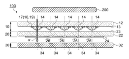
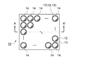
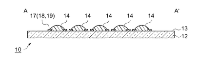
図1は、マイクロレンズ基板、及びマイクロレンズ基板を備えた撮像装置の構造を示す模式断面図である。図2は、マイクロレンズ基板における遮光基板との対向面の平面図である。図3は、図2におけるマイクロレンズ基板のA−A'線に沿う断面図である。以下、マイクロレンズ基板、及びマイクロレンズ基板を備えた撮像装置(及び電子機器)の構造を、図1〜図3を参照しながら説明する。
<Configuration of microlens substrate, imaging device, and electronic device>
FIG. 1 is a schematic cross-sectional view illustrating the structure of a microlens substrate and an imaging apparatus including the microlens substrate. FIG. 2 is a plan view of the surface of the microlens substrate that faces the light-shielding substrate. FIG. 3 is a cross-sectional view taken along line AA ′ of the microlens substrate in FIG. Hereinafter, the structure of the microlens substrate and the imaging device (and electronic apparatus) including the microlens substrate will be described with reference to FIGS.
図1に示すように、撮像装置100は、認証処理のために生体(例えば、指)200の静脈像を撮像する、例えば、電子機器としての生体認証装置(静脈センサー)に用いられるものであり、マイクロレンズ基板10と遮光基板20と受光基板30とを具備する。マイクロレンズ基板10は、受光基板30と生体200との間に介在し、遮光基板20はマイクロレンズ基板10と受光基板30との間に介在する。
As shown in FIG. 1, the
図1〜図3に示すように、マイクロレンズ基板10は、基板12と複数のマイクロレンズ14と複数の下地パターン17とを含んで構成される。基板12は、例えばガラス基板等の光透過性の板状部材である。
As shown in FIGS. 1 to 3, the
複数のマイクロレンズ14の各々は、入射光を集光する凸レンズであり、図2に示すように、基板12の表面13にアレイ状に配列している。複数の下地パターン17の各々は、基板12の表面13にマイクロレンズ14毎に配置されている。
Each of the plurality of
各下地パターン17は、図2に示すように、平面視でマイクロレンズ14を包囲する円環状のパターンであり、光反射性を有する反射膜18と、光の反射を抑える反射防止膜19とが積層されている。なお、反射防止膜19は、生体200側に配置されており、反射膜18からの反射光によってノイズが発生することを防いでいる。
As shown in FIG. 2, each
図1に示す遮光基板20は、光透過性の基板22と、基板22の表面に形成された遮光層24とを含んで構成されている。遮光層24は、遮光性の材料で形成される。遮光層24のうち各マイクロレンズ14の光軸に対応する箇所には開口部26が形成されている。
The
マイクロレンズ基板10と遮光基板20とは、図示しないスペーサーを介して、相互に対向して配置されている。よって、マイクロレンズ14は、基板22の表面23に対して間隔をあけて対向配置されている。
The
図1に示す受光基板30は、基板32と、基板32の表面に形成された複数の受光素子34とを含んで構成されている。また、受光基板30は、遮光基板20に対して間隔をあけて対向している。各受光素子34は、マイクロレンズ14の光軸に対応する位置に形成され、入射光の光量に応じた検出信号を生成する。
The
以上の構成において、図1に矢印αで示すように、所定の位置(例えば、生体200を挟んでマイクロレンズ基板10とは反対側)に配置された光源(図示略)による照射光が生体200の内部の静脈にて透過または反射して基板12に入射する。照射光は、各マイクロレンズ14で集光されたうえで遮光層24の開口部26を通過して、受光素子34に到達する。すなわち、生体200の静脈像が撮像される。
In the above configuration, as indicated by an arrow α in FIG. 1, the light emitted from a light source (not shown) disposed at a predetermined position (for example, on the side opposite to the
<マイクロレンズ基板の製造方法>
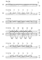
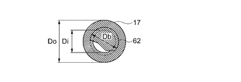
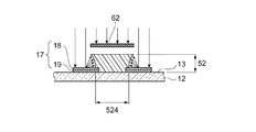
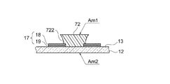
図4は、マイクロレンズ基板の製造方法を工程順に示す模式断面図である。図5は、下地パターンとマスクの遮光部との平面的な位置関係を示す模式平面図である。図6及び図7は、製造方法のうち一部の工程を示す模式断面図である。以下、マイクロレンズ基板の製造方法を、図4〜図7を参照しながら説明する。
<Method of manufacturing microlens substrate>
FIG. 4 is a schematic cross-sectional view showing a method of manufacturing a microlens substrate in the order of steps. FIG. 5 is a schematic plan view showing a planar positional relationship between the base pattern and the light shielding portion of the mask. 6 and 7 are schematic cross-sectional views showing some steps in the manufacturing method. Hereinafter, a method for manufacturing the microlens substrate will be described with reference to FIGS.
まず、図4(a)に示す工程では、基板12上に、後に下地パターン17となる反射膜18a(反射膜前駆体膜)及び反射防止膜19aを形成する。具体的には、基板12の表面13に光の反射を抑える反射防止膜19aを形成し、反射防止膜19a上に光反射性の反射膜18aを形成する。
First, in the step shown in FIG. 4A, a
反射膜18aの材料としては、例えば、アルミニウム(Al)や銀(Ag)や金(Au)等の高反射性の金属材料が好適である。反射防止膜19aの材料としては、例えば、チタン(Ti)やモリブデン(Mo)や有機系材料(例えば、アクリル系樹脂30%を含む有機溶媒のアクリル系樹脂)などが挙げられる。
As the material of the
また、反射膜18a及び反射防止膜19aの形成方法としては、スパッタリング法や真空蒸着法やCVD(Chemical Vapor Deposition)法等の、公知の成膜技術が任意に採用される。
In addition, as a method for forming the
次に、図4(b)に示す工程(反射膜形成工程)では、基板12上に下地パターン17を形成する。具体的には、基板12の表面13のうちマイクロレンズ14が形成されるべき領域を包囲するように、反射膜18及び反射防止膜19を有する円環状の下地パターン17を形成する。下地パターン17の形成方法としては、例えば、フォトリソグラフィ技術等の公知のパターニング技術を用いることができる。なお、マスク蒸着等の方法で基板12の表面13に直接的に複数の下地パターン17を形成することも可能である。
Next, in a step (reflection film forming step) shown in FIG. 4B, a
次に、図4(c)に示す工程(感光層形成工程)では、基板12上に感光層52を形成する。具体的には、下地パターン17が形成された基板12の表面13の全域を覆うように感光層52を形成する。感光層52は、露光部分が除去されるポジ型の感光性材料を用いる。具体的には、アクリルやポリイミド等の高分子樹脂材料が感光層52の材料として好適である。感光層52の形成方法としては、例えば、スピンコート法やロールコート法等の公知の成膜技術を用いることができる。
Next, in the step shown in FIG. 4C (photosensitive layer forming step), the
次に、図4(d)に示す工程(露光工程)では、感光層52を露光する。具体的には、感光層52を挟んで基板12とは反対側から、感光層52を選択的に露光する。感光層52の露光には、例えば、遮光部62を有するマスク60が使用される。遮光部62は、感光層52のうち、マイクロレンズ14に対応する各領域(マイクロレンズ14が形成されるべき領域)522に重なる部分に配置されている。つまり、感光層52のうち、領域522を除外した領域が露光される。
Next, in the step (exposure step) shown in FIG. 4D, the
なお、図5に示すように、遮光部62は、直径Dbの円形状に形成されて円環状の下地パターン17と同心に配置される。直径Dbは、下地パターン17の内径(マイクロレンズ14に対応する領域522の略直径)Di以上の寸法で下地パターン17の外径Doを下回る寸法に選定される。したがって、遮光部62の周縁は、平面視で下地パターン17の内周縁と外周縁との間に位置する。
As shown in FIG. 5, the
遮光部62の周縁が反射膜18の内周縁と外周縁との間に位置するから、露光工程において、感光層52のうちマイクロレンズ14に対応する領域の周縁に、反射膜18の表面からの反射光を充分に照射することが可能である。
Since the periphery of the
次に、図4(e)に示す工程(現像工程)では、感光層52を現像(パターニング)する。具体的には、感光層52のうち、図4(d)に示す工程で露光された領域が除去される。これにより、基板12上に、遮光部62で遮光された領域522に対応する複数のマイクロレンズ前駆体72が形成される。
Next, in the step (development step) shown in FIG. 4E, the
具体的には、図6に示すように、マスク60(遮光部62)を透過して、感光層52のうち領域524に入射した光は、感光層52の内部を直進したうえで下地パターン17に到達し、下地パターン17を構成する反射膜18の表面で反射(散乱)する。
Specifically, as shown in FIG. 6, the light that has passed through the mask 60 (light-shielding portion 62) and entered the
下地パターン17の表面での反射光は、感光層52のうち領域524の周縁部に照射される。よって、図7に示すように、マイクロレンズ前駆体72の側面722は、表面13から離れた位置ほど、マイクロレンズ前駆体72の直径(断面積)が増加するように、表面13に対して傾斜する。
The reflected light from the surface of the
すなわち、マイクロレンズ前駆体72の上面の面積Am1は、底面の面積(すなわち下地パターン17の内側の面積)Am2を上回る。概略的には、表面13に垂直な断面でのマイクロレンズ前駆体72の断面形状は、上底が下底を上回る逆台形状となる。
That is, the area Am1 of the top surface of the
次に、図4(f)に示す工程(加熱工程)では、基板12上にマイクロレンズ14を完成させる。具体的には、マイクロレンズ前駆体72を加熱(リフロー処理)することで軟化(溶融)させる。マイクロレンズ前駆体72は、加熱により流動し、表面張力の作用で表面が曲面状に変形する。このとき、底面の面積Am2(図7参照)は、殆ど変わらない。その後、マイクロレンズ前駆体72を冷却することにより、マイクロレンズ14が完成する。
Next, in the process (heating process) shown in FIG. 4F, the
熱処理の温度は、例えば、150℃〜250℃である。以上の工程によって製造されたマイクロレンズ基板10と、別途製造された遮光基板20とが、図1のように相互に対向して配置される。
The temperature of heat processing is 150 degreeC-250 degreeC, for example. The
図6及び図7を参照して説明したように、リフロー処理(加熱)を施した際、下地パターン17によってマイクロレンズ14の底面の面積Am2を略固定することが可能となるので、マイクロレンズ14の表面の曲率を、従来と比較して小さくすることができる。その結果、マイクロレンズ14の設計範囲を広げることができる。
As described with reference to FIGS. 6 and 7, when the reflow process (heating) is performed, the area Am <b> 2 of the bottom surface of the
図8は、マイクロレンズの半径とマイクロレンズの高さとの関係を、マイクロレンズ前駆体の膜厚別に示すグラフである。以下、マイクロレンズの半径とマイクロレンズの高さとの関係を、図8を参照しながら説明する。 FIG. 8 is a graph showing the relationship between the radius of the microlens and the height of the microlens according to the thickness of the microlens precursor. Hereinafter, the relationship between the radius of the microlens and the height of the microlens will be described with reference to FIG.
図8に示すように、グラフの横軸は、マイクロレンズ14の半径値を示しており、図示右側にいくに従って半径値が大きくなっていることを示している。グラフの縦軸は、マイクロレンズ14の高さを示しており、図示上側にいくに従って高さが高くなっていることを示している。このようなマイクロレンズ14の半径値と高さとの関係を、マイクロレンズ前駆体72の膜厚毎に示している。
As shown in FIG. 8, the horizontal axis of the graph indicates the radius value of the
グラフAは、マイクロレンズ前駆体72の厚みが5.0μmであり、下地パターン17が形成されていない場合のマイクロレンズを測定したものである。グラフBは、マイクロレンズ前駆体72の厚みが5.0μmであり、下地パターン17が形成されている場合のマイクロレンズ14を測定したものである。
Graph A is a measurement of the microlens when the thickness of the
グラフCは、マイクロレンズ前駆体72の厚みが3.5μmであり、下地パターン17が形成されていない場合のマイクロレンズを測定したものである。グラフDは、マイクロレンズ前駆体72の厚みが3.5μmであり、下地パターン17が形成されている場合のマイクロレンズ14を測定したものである。
Graph C is a measurement of the microlens when the thickness of the
以上のように、マイクロレンズ前駆体72の厚みが5.0μmの場合、下地パターン17を構成する反射膜18及び反射防止膜19を設けた場合の方が、従来のマイクロレンズの半径値と比較して、小さな半径値(曲率)のマイクロレンズを形成することが可能となる。これにより、従来のマイクロレンズの設計範囲と比較して、設計範囲を拡大することができる。
As described above, when the thickness of the
一方、マイクロレンズ前駆体72の厚みが3.5μmの場合も同様に、下地パターン17を構成する反射膜18及び反射防止膜19を設けた場合の方が、従来のマイクロレンズの半径値と比較して、小さな半径値(曲率)のマイクロレンズを形成することが可能となる。これにより、従来のマイクロレンズの設計範囲と比較して、設計範囲を拡大することができる。
On the other hand, when the thickness of the
また、下地パターン17を形成することにより、所望の曲率のマイクロレンズ14を形成することができるので、膜厚(マイクロレンズ前駆体72の膜厚)を細かく管理したり、材料を選定したりすることを省略することができ、マイクロレンズ基板10の製造工程を簡素化することが可能である。
In addition, since the
<生体認証装置>
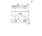
次に、上記実施形態の撮像装置を備えた生体認証装置の例につき、図9を参照して説明する。図9は生体認証装置の構成を示すブロック図である。
<Biometric authentication device>
Next, an example of a biometric authentication device including the imaging device of the above embodiment will be described with reference to FIG. FIG. 9 is a block diagram showing the configuration of the biometric authentication apparatus.
図9に示すように、本実施形態の生体認証装置80は、記憶部81、撮像部82、発光部83、認証実行部84、およびこれら各部を制御する制御部85を有する。撮像部82、発光部83は撮像装置100に相当し、撮像部82はマイクロレンズ基板10、遮光基板20、受光基板30を含むものであり、発光部83は光源に相当する。
As illustrated in FIG. 9, the
発光部83は、制御部85から伝達される信号に基づいて、光(近赤外光)を指に向けて射出する。撮像部82は、制御部85から伝達される制御信号に基づいて撮影動作を開始し、撮像された静脈パターンを制御部85に出力する。
The
制御部85は、記憶部81に格納されたプログラムに基づいて信号の演算処理、信号伝送といった各種の処理を実行し、撮像部82から出力される静脈パターンを認証実行部84に伝達する。
The
記憶部81は、ハードディスク、半導体メモリー(DRAM(Dynamic Random Access Memory)、またはSRAM(Static Random Access Memory))といった記憶装置である。記憶部81には、生体認証を実現するためのプログラム、画像構成を実現するためのプログラム、認証時に用いられる予め登録された静脈パターン、および認証履歴といった情報が格納される。
The
認証実行部84は、撮像部82によって撮像され出力された静脈パターン(画像情報)と予め登録された生体の静脈パターン(画像情報)とを照合して、撮像された静脈パターンが登録された生体のものか否か判定する。静脈認証の方法は、静脈パターンの類似性を判別する各種方法に依存する。
The
生体認証装置80は、上記実施形態の撮像装置100を備えているので、指の内部における静脈パターン(生体情報)を鮮明な状態で入手することができる。したがって、認証実行部84は、予め登録された静脈パターンごとに、撮像された静脈パターンとの間で類似性を判別し、高い認証精度を実現することができる。また、より高い認証精度を実現し、不正行為を防止することができる。
Since the
<電子機器>
次に本実施形態の電子機器について、図10を参照して説明する。図10(a)は電子機器としての携帯型電話機を示す斜視図、同図(b)は電子機器としてのパーソナルコンピューターを示す概略図である。
<Electronic equipment>
Next, the electronic apparatus of this embodiment will be described with reference to FIG. FIG. 10A is a perspective view showing a mobile phone as an electronic device, and FIG. 10B is a schematic view showing a personal computer as an electronic device.
図10(a)に示すように、本実施形態の電子機器としての携帯型電話機300は、表示部301、操作ボタン302および生体認証装置80を備えている。生体認証装置80は、携帯型電話機300の本体に搭載された撮像装置100に指を触れさせることによって取得された静脈パターンを用いて、例えば、携帯型電話機300のロック状態を解除したり、金融決済の際の個人認証を行うことができる。
As shown in FIG. 10A, a
図10(b)に示すように、本実施形態の電子機器としてのノート型のパーソナルコンピューター400は、表示部411、入力ボタン412および生体認証装置80を備えている。生体認証装置80は、パーソナルコンピューター400の本体に組み込まれた撮像装置100に指を触れさせることによって取得された静脈パターンを用い、例えば、パーソナルコンピューター400にログインしたり、金融決済の際の個人認証を行うことができる。
As shown in FIG. 10B, a notebook
上記携帯型電話機300および上記パーソナルコンピューター400は、室内、屋外を問わず静脈パターンを撮影できる撮像装置100を有する生体認証装置80を備えているため、あらゆる環境下で高精度に個人認証を行うことができる。それゆえに、不正な使用行為を防止することができる。
Since the
以上詳述したように、本実施形態のマイクロレンズ基板10の製造方法、マイクロレンズ基板10の製造方法を用いて製造されたマイクロレンズ基板10を備えた撮像装置100、及びその撮像装置100を備えた電子機器によれば、以下に示す効果が得られる。
As described above in detail, the manufacturing method of the
(1)本実施形態のマイクロレンズ基板10の製造方法によれば、マイクロレンズ14が形成される領域522の周囲に反射膜18を有する下地パターン17を形成するので、露光工程において反射膜18の表面で反射した光の照射により、反射膜18の略縁を外形とする逆台形の形状に感光層52を露光することができる。よって、反射膜18を形成しない場合と比較して、加熱工程における感光層52の高さを増加させることが可能となり、マイクロレンズ14の曲率半径を小さくすることができる。その結果、マイクロレンズ前駆体72の膜厚を調整したり、感光層52の材料を選定したりすることなく、マイクロレンズ14の曲率半径の範囲(設計範囲)を拡大することができる。加えて、下地パターン17の大きさを変えたり、反射膜18を形成しなかったりすることにより、同じプロセスであっても、面内に異なる曲率をもったマイクロレンズ14を容易に形成することができる。
(1) According to the method for manufacturing the
(2)本実施形態のマイクロレンズ基板10の製造方法によれば、反射防止膜19上に反射膜18を形成するので、露光工程において、反射防止膜19の基板側の光が乱反射することを抑えることができる。よって、マイクロレンズ14の曲率がばらつくことを抑えることができる。
(2) According to the manufacturing method of the
(3)本実施形態のマイクロレンズ14を備えた撮像装置100によれば、マイクロレンズ14の曲率半径の範囲を拡大することが可能になり、例えば、曲率半径が小さい場合、焦点距離を短くすることが可能となり、その結果、薄型の撮像装置100を提供することができる。加えて、1枚の基板に焦点深度の異なるマイクロレンズ14を備えた撮像装置100を提供することができる。
(3) According to the
(4)本実施形態の電子機器によれば、上記した撮像装置100を備えているので、薄型の電子機器を提供することができたり、広範囲の距離を撮像することが可能な電子機器を提供することができる。
(4) According to the electronic apparatus of the present embodiment, since the above-described
なお、実施形態は上記に限定されず、以下のような形態で実施することもできる。 In addition, embodiment is not limited above, It can also implement with the following forms.
(変形例1)
上記したように、下地パターン17は、マイクロレンズ14が形成される領域を包囲する円環状のパターンであることに限定されず、例えば、図11に示すように、マイクロレンズ14が形成される領域を除く全ての領域に形成するようにしてもよい。
(Modification 1)
As described above, the
図11は、マイクロレンズ基板(下地パターン)の構造を示す模式平面図である。図11に示すマイクロレンズ基板110の下地パターン117は、基板112上に反射防止膜119が形成されており、反射防止膜119上に反射膜118が形成されている。つまり、マイクロレンズ14が形成される領域のみ下地パターン117が形成されてない。
FIG. 11 is a schematic plan view showing the structure of the microlens substrate (underlying pattern). In the base pattern 117 of the
これによれば、上記した実施形態の効果に加えて、マイクロレンズ14間に、別途BMを配置することなく、BMを配置した場合と同じ効果を得ることができる。また、光反射性の高い材料を多く用いており、熱の伝達が早く蓄熱作用があるため、加熱(リフロー処理)時にマイクロレンズの形状を均一にすることができる。
According to this, in addition to the effect of the above-described embodiment, the same effect as when the BM is arranged can be obtained without separately arranging the BM between the
(変形例2)
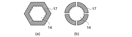
上記したように、下地パターン17は、平面的に連続した円環状に形成することに限定されず、例えば、図12に示すような形状であってもよい。図12は、下地パターンの変形例の構造を示す模式平面図である。
(Modification 2)
As described above, the
図12(a)に示す下地パターン17は、マイクロレンズ14が形成される領域を多角形(例えば、六角形)の環状に形成している。また、図12(b)に示す下地パターン17は、閉じた環状の形状ではなく、複数に離間する円環形状に形成している。
In the
なお、感光層52のうち領域524(図6参照)の周縁に下地パターン17での反射光を均一に照射するという観点からすると、下地パターン17を閉じた形状(例えば円形や多角形の環状)に形成した構成が好適である。
From the viewpoint of uniformly irradiating the periphery of the region 524 (see FIG. 6) of the
(変形例3)
上記したように、下地パターン17は、反射膜18と反射防止膜19との積層構成であることに限定されず、例えば、反射膜18のみの構成であってもよい。この構成によれば、比較的に乱反射が少ない場合に適用することが可能となり、製造工程を簡略化することができる。
(Modification 3)
As described above, the
(変形例4)
上記したように、下地パターン17を形成する方法として、下地パターン17のために反射防止膜19aと反射膜18aを積層してパターニングする方法に限定されず、例えば、貼り合わせ時のマークの形成に用いた形成層を下地パターン17として適用するようにしてもよい。この方法によれば、下地パターン17とアライメントマークとが共通の工程で形成されるから、下地パターン17とアライメントマークとを別工程で形成する場合と比較してマイクロレンズ基板10の製造工程を簡素化することができる。
(Modification 4)
As described above, the method of forming the
10,110…マイクロレンズ基板、12,22,112…基板、13…表面、14…マイクロレンズ、17,117…下地パターン、18,18a,118…反射膜、19,19a,119…反射防止膜、20…遮光基板、23…表面、24…遮光層、26…開口部、30…受光基板、32…基板、34…受光素子、52…感光層、60…マスク、62…遮光部、72…マイクロレンズ前駆体、80…生体認証装置、81…記憶部、82…撮像部、83…発光部、84…認証実行部、85…制御部、100…撮像装置、112…基板、200…生体、300…携帯型電話機、301,411…表示部、302…操作ボタン、400…パーソナルコンピューター、412…入力ボタン、522,524…領域、722…側面。 DESCRIPTION OF SYMBOLS 10,110 ... Microlens board | substrate, 12, 22, 112 ... Board | substrate, 13 ... Surface, 14 ... Microlens, 17,117 ... Base pattern, 18, 18a, 118 ... Reflective film, 19, 19a, 119 ... Antireflection film , 20 ... light shielding substrate, 23 ... surface, 24 ... light shielding layer, 26 ... opening, 30 ... light receiving substrate, 32 ... substrate, 34 ... light receiving element, 52 ... photosensitive layer, 60 ... mask, 62 ... light shielding portion, 72 ... Microlens precursor, 80 ... biometric authentication device, 81 ... storage unit, 82 ... imaging unit, 83 ... light emitting unit, 84 ... authentication execution unit, 85 ... control unit, 100 ... imaging device, 112 ... substrate, 200 ... biological body, 300 ... mobile phone, 301,411 ... display unit, 302 ... operation button, 400 ... personal computer, 412 ... input button, 522,524 ... area, 722 ... side.
Claims (8)
前記反射膜が形成された前記基板上にポジ型の感光性材料で感光層を形成する感光層形成工程と、
前記感光層のうち前記マイクロレンズに対応する領域以外の領域を、前記感光層を挟んで前記基板とは反対側から露光する露光工程と、
露光された前記感光性材料を現像する現像工程と、
前記感光性材料の表面を加熱により曲面状に変形させることで前記マイクロレンズを形成する加熱工程と、
を含むことを特徴とするマイクロレンズ基板の製造方法。 A reflective film forming step of forming a reflective film with a reflective material around a region of the substrate where the microlens is formed;
A photosensitive layer forming step of forming a photosensitive layer with a positive photosensitive material on the substrate on which the reflective film is formed;
An exposure step of exposing a region other than the region corresponding to the microlens in the photosensitive layer from the opposite side of the substrate with the photosensitive layer interposed therebetween;
A development step of developing the exposed photosensitive material;
A heating step of forming the microlens by deforming the surface of the photosensitive material into a curved surface by heating;
A method for manufacturing a microlens substrate, comprising:
前記反射膜形成工程は、前記基板上の反射防止膜上に前記反射膜を形成することを特徴とするマイクロレンズ基板の製造方法。 A method of manufacturing a microlens substrate according to claim 1,
The method of manufacturing a microlens substrate, wherein the reflecting film forming step forms the reflecting film on an antireflection film on the substrate.
前記反射膜形成工程は、前記マイクロレンズが形成される領域を包囲する閉じた形状に前記反射膜を形成することを特徴とするマイクロレンズ基板の製造方法。 A method of manufacturing a microlens substrate according to claim 1 or 2,
The method of manufacturing a microlens substrate, wherein the reflecting film forming step forms the reflecting film in a closed shape surrounding a region where the microlens is formed.
前記反射膜形成工程では、前記反射膜を円環状に形成することを特徴とするマイクロレンズ基板の製造方法。 A method of manufacturing a microlens substrate according to claim 3,
In the reflective film forming step, the reflective film is formed in an annular shape.
前記露光工程は、前記マイクロレンズに対応する領域に遮光部が重なるマスクを使用し、
前記遮光部の周縁は、前記反射膜の内周縁と外周縁との間に位置することを特徴とするマイクロレンズ基板の製造方法。 A method of manufacturing a microlens substrate according to any one of claims 1 to 4,
The exposure step uses a mask in which a light shielding portion overlaps an area corresponding to the microlens,
The manufacturing method of a microlens substrate, wherein a peripheral edge of the light shielding portion is located between an inner peripheral edge and an outer peripheral edge of the reflective film.
前記反射膜形成工程は、前記基板を覆う光反射性の反射膜前駆体膜を形成する工程と、
前記反射膜前駆体膜を選択的に除去することで、前記反射膜と、前記マイクロレンズ基板の位置合わせに使用されるアライメントマークとを一括的に形成する工程とを含むことを特徴とするマイクロレンズ基板の製造方法。 A method of manufacturing a microlens substrate according to any one of claims 1 to 5,
The reflective film forming step includes a step of forming a light reflective reflective film precursor film covering the substrate;
And a step of collectively forming the reflective film and an alignment mark used for alignment of the microlens substrate by selectively removing the reflective film precursor film. A method for manufacturing a lens substrate.
Priority Applications (1)
| Application Number | Priority Date | Filing Date | Title |
|---|---|---|---|
| JP2011125104A JP2012252183A (en) | 2011-06-03 | 2011-06-03 | Manufacturing method for microlens substrate, image pickup device including microlens substrate manufactured using manufacturing method for microlens substrate, and electronic apparatus including image pickup device |
Applications Claiming Priority (1)
| Application Number | Priority Date | Filing Date | Title |
|---|---|---|---|
| JP2011125104A JP2012252183A (en) | 2011-06-03 | 2011-06-03 | Manufacturing method for microlens substrate, image pickup device including microlens substrate manufactured using manufacturing method for microlens substrate, and electronic apparatus including image pickup device |
Publications (2)
| Publication Number | Publication Date |
|---|---|
| JP2012252183A true JP2012252183A (en) | 2012-12-20 |
| JP2012252183A5 JP2012252183A5 (en) | 2014-07-17 |
Family
ID=47525050
Family Applications (1)
| Application Number | Title | Priority Date | Filing Date |
|---|---|---|---|
| JP2011125104A Withdrawn JP2012252183A (en) | 2011-06-03 | 2011-06-03 | Manufacturing method for microlens substrate, image pickup device including microlens substrate manufactured using manufacturing method for microlens substrate, and electronic apparatus including image pickup device |
Country Status (1)
| Country | Link |
|---|---|
| JP (1) | JP2012252183A (en) |
Cited By (2)
| Publication number | Priority date | Publication date | Assignee | Title |
|---|---|---|---|---|
| KR101547155B1 (en) * | 2014-03-03 | 2015-08-26 | 한국과학기술원 | Batch Fabrication Method of Three-dimensional Photonic Microstructures |
| US10068915B2 (en) | 2015-03-03 | 2018-09-04 | Toshiba Memory Corporation | Manufacturing method for a semiconductor device including resist films different in thickness |
Citations (12)
| Publication number | Priority date | Publication date | Assignee | Title |
|---|---|---|---|---|
| JPH03173472A (en) * | 1989-12-01 | 1991-07-26 | Mitsubishi Electric Corp | Method of forming microlens |
| JPH07174902A (en) * | 1993-12-17 | 1995-07-14 | Ricoh Opt Ind Co Ltd | Microlens array and its production |
| JPH08313706A (en) * | 1995-05-12 | 1996-11-29 | Hoya Corp | Microlens array integrated with light-shielding part and its production |
| JPH1098173A (en) * | 1996-09-25 | 1998-04-14 | Sony Corp | Method of forming on-chip micro lens |
| JP2000075106A (en) * | 1998-08-27 | 2000-03-14 | Seiko Epson Corp | Microlens array, method of manufacturing the same, and display device |
| JP2003172917A (en) * | 2001-09-28 | 2003-06-20 | Hoya Corp | Counter substrate for liquid crystal display panel and manufacturing method therefor |
| JP2005012189A (en) * | 2003-05-28 | 2005-01-13 | Canon Inc | Photoelectric conversion device and manufacturing method thereof |
| JP2006071981A (en) * | 2004-09-02 | 2006-03-16 | Fuji Photo Film Co Ltd | Micro lens array, optical member, and manufacturing method of micro lens array |
| JP2006267866A (en) * | 2005-03-25 | 2006-10-05 | Fuji Photo Film Co Ltd | Manufacturing method of microlens array |
| JP2007187759A (en) * | 2006-01-11 | 2007-07-26 | Seiko Epson Corp | Microlens substrate manufacturing method, microlens substrate, transmissive screen, and rear projector |
| JP2008036058A (en) * | 2006-08-04 | 2008-02-21 | Hitachi Maxell Ltd | Imaging device and biometric authentication device |
| JP2012198452A (en) * | 2011-03-23 | 2012-10-18 | Seiko Epson Corp | Manufacturing method of microlens substrate |
-
2011
- 2011-06-03 JP JP2011125104A patent/JP2012252183A/en not_active Withdrawn
Patent Citations (12)
| Publication number | Priority date | Publication date | Assignee | Title |
|---|---|---|---|---|
| JPH03173472A (en) * | 1989-12-01 | 1991-07-26 | Mitsubishi Electric Corp | Method of forming microlens |
| JPH07174902A (en) * | 1993-12-17 | 1995-07-14 | Ricoh Opt Ind Co Ltd | Microlens array and its production |
| JPH08313706A (en) * | 1995-05-12 | 1996-11-29 | Hoya Corp | Microlens array integrated with light-shielding part and its production |
| JPH1098173A (en) * | 1996-09-25 | 1998-04-14 | Sony Corp | Method of forming on-chip micro lens |
| JP2000075106A (en) * | 1998-08-27 | 2000-03-14 | Seiko Epson Corp | Microlens array, method of manufacturing the same, and display device |
| JP2003172917A (en) * | 2001-09-28 | 2003-06-20 | Hoya Corp | Counter substrate for liquid crystal display panel and manufacturing method therefor |
| JP2005012189A (en) * | 2003-05-28 | 2005-01-13 | Canon Inc | Photoelectric conversion device and manufacturing method thereof |
| JP2006071981A (en) * | 2004-09-02 | 2006-03-16 | Fuji Photo Film Co Ltd | Micro lens array, optical member, and manufacturing method of micro lens array |
| JP2006267866A (en) * | 2005-03-25 | 2006-10-05 | Fuji Photo Film Co Ltd | Manufacturing method of microlens array |
| JP2007187759A (en) * | 2006-01-11 | 2007-07-26 | Seiko Epson Corp | Microlens substrate manufacturing method, microlens substrate, transmissive screen, and rear projector |
| JP2008036058A (en) * | 2006-08-04 | 2008-02-21 | Hitachi Maxell Ltd | Imaging device and biometric authentication device |
| JP2012198452A (en) * | 2011-03-23 | 2012-10-18 | Seiko Epson Corp | Manufacturing method of microlens substrate |
Cited By (2)
| Publication number | Priority date | Publication date | Assignee | Title |
|---|---|---|---|---|
| KR101547155B1 (en) * | 2014-03-03 | 2015-08-26 | 한국과학기술원 | Batch Fabrication Method of Three-dimensional Photonic Microstructures |
| US10068915B2 (en) | 2015-03-03 | 2018-09-04 | Toshiba Memory Corporation | Manufacturing method for a semiconductor device including resist films different in thickness |
Similar Documents
| Publication | Publication Date | Title |
|---|---|---|
| JP2012245083A (en) | Imaging device, biometric authentication device, electronic equipment | |
| JP6945561B2 (en) | Display panel and display device | |
| TWI650875B (en) | Integrated sensing module, integrated sensing component and manufacturing method thereof | |
| CN107103307A (en) | Contact panel and display device | |
| CN110088768A (en) | Under-screen fingerprint recognition device and electronic equipment | |
| CN108133174B (en) | Optical image sensor and flat panel display embedded with the same | |
| CN211427367U (en) | Fingerprint identification device and electronic equipment | |
| US20180175125A1 (en) | Image capturing apparatus | |
| WO2017118067A1 (en) | Optical-type fingerprint identification display screen and display device | |
| CN111414830B (en) | Fingerprint detection device, touch panel and electronic device | |
| TW201224542A (en) | Optical sensing module | |
| TWI756056B (en) | Sensing device | |
| WO2020113396A1 (en) | Optical lens and manufacturing method therefor, fingerprint recognition module, and mobile terminal | |
| CN110945527B (en) | Fingerprint identification device and electronic equipment | |
| CN110164882B (en) | Optical sensor and method for manufacturing the same | |
| US20200381470A1 (en) | Image capture device | |
| CN111801684A (en) | Fingerprint detection devices and electronic equipment | |
| WO2021022560A1 (en) | Fingerprint detection apparatus and electronic device | |
| JP5708108B2 (en) | Manufacturing method of microlens substrate | |
| JP2012252183A (en) | Manufacturing method for microlens substrate, image pickup device including microlens substrate manufactured using manufacturing method for microlens substrate, and electronic apparatus including image pickup device | |
| CN111814723A (en) | A display device and method of making the same | |
| CN210983441U (en) | imaging device | |
| JP2012252259A (en) | Lens array, image pickup apparatus, biometric authentication apparatus, and electronic apparatus | |
| KR102942582B1 (en) | Fingerprint recognition devices and electronic devices | |
| KR102396510B1 (en) | Pin hole pattern film and method for manufacturing thereof |
Legal Events
| Date | Code | Title | Description |
|---|---|---|---|
| A521 | Written amendment |
Free format text: JAPANESE INTERMEDIATE CODE: A523 Effective date: 20140602 |
|
| A621 | Written request for application examination |
Free format text: JAPANESE INTERMEDIATE CODE: A621 Effective date: 20140602 |
|
| RD04 | Notification of resignation of power of attorney |
Free format text: JAPANESE INTERMEDIATE CODE: A7424 Effective date: 20150107 |
|
| A977 | Report on retrieval |
Free format text: JAPANESE INTERMEDIATE CODE: A971007 Effective date: 20150423 |
|
| A131 | Notification of reasons for refusal |
Free format text: JAPANESE INTERMEDIATE CODE: A131 Effective date: 20150428 |
|
| A521 | Written amendment |
Free format text: JAPANESE INTERMEDIATE CODE: A523 Effective date: 20150625 |
|
| A131 | Notification of reasons for refusal |
Free format text: JAPANESE INTERMEDIATE CODE: A131 Effective date: 20151117 |
|
| A761 | Written withdrawal of application |
Free format text: JAPANESE INTERMEDIATE CODE: A761 Effective date: 20160107 |