JP2012253145A - Detector, exposure apparatus and manufacturing method of device - Google Patents
Detector, exposure apparatus and manufacturing method of device Download PDFInfo
- Publication number
- JP2012253145A JP2012253145A JP2011123586A JP2011123586A JP2012253145A JP 2012253145 A JP2012253145 A JP 2012253145A JP 2011123586 A JP2011123586 A JP 2011123586A JP 2011123586 A JP2011123586 A JP 2011123586A JP 2012253145 A JP2012253145 A JP 2012253145A
- Authority
- JP
- Japan
- Prior art keywords
- wavelength band
- light
- substrate
- subject
- wavelength
- Prior art date
- Legal status (The legal status is an assumption and is not a legal conclusion. Google has not performed a legal analysis and makes no representation as to the accuracy of the status listed.)
- Granted
Links
Images


Classifications
-
- G—PHYSICS
- G02—OPTICS
- G02B—OPTICAL ELEMENTS, SYSTEMS OR APPARATUS
- G02B5/00—Optical elements other than lenses
- G02B5/20—Filters
- G02B5/201—Filters in the form of arrays
-
- G—PHYSICS
- G03—PHOTOGRAPHY; CINEMATOGRAPHY; ANALOGOUS TECHNIQUES USING WAVES OTHER THAN OPTICAL WAVES; ELECTROGRAPHY; HOLOGRAPHY
- G03B—APPARATUS OR ARRANGEMENTS FOR TAKING PHOTOGRAPHS OR FOR PROJECTING OR VIEWING THEM; APPARATUS OR ARRANGEMENTS EMPLOYING ANALOGOUS TECHNIQUES USING WAVES OTHER THAN OPTICAL WAVES; ACCESSORIES THEREFOR
- G03B27/00—Photographic printing apparatus
- G03B27/32—Projection printing apparatus, e.g. enlarger, copying camera
- G03B27/52—Details
- G03B27/53—Automatic registration or positioning of originals with respect to each other or the photosensitive layer
-
- G—PHYSICS
- G03—PHOTOGRAPHY; CINEMATOGRAPHY; ANALOGOUS TECHNIQUES USING WAVES OTHER THAN OPTICAL WAVES; ELECTROGRAPHY; HOLOGRAPHY
- G03F—PHOTOMECHANICAL PRODUCTION OF TEXTURED OR PATTERNED SURFACES, e.g. FOR PRINTING, FOR PROCESSING OF SEMICONDUCTOR DEVICES; MATERIALS THEREFOR; ORIGINALS THEREFOR; APPARATUS SPECIALLY ADAPTED THEREFOR
- G03F9/00—Registration or positioning of originals, masks, frames, photographic sheets or textured or patterned surfaces, e.g. automatically
- G03F9/70—Registration or positioning of originals, masks, frames, photographic sheets or textured or patterned surfaces, e.g. automatically for microlithography
- G03F9/7065—Production of alignment light, e.g. light source, control of coherence, polarization, pulse length, wavelength
-
- G—PHYSICS
- G03—PHOTOGRAPHY; CINEMATOGRAPHY; ANALOGOUS TECHNIQUES USING WAVES OTHER THAN OPTICAL WAVES; ELECTROGRAPHY; HOLOGRAPHY
- G03F—PHOTOMECHANICAL PRODUCTION OF TEXTURED OR PATTERNED SURFACES, e.g. FOR PRINTING, FOR PROCESSING OF SEMICONDUCTOR DEVICES; MATERIALS THEREFOR; ORIGINALS THEREFOR; APPARATUS SPECIALLY ADAPTED THEREFOR
- G03F9/00—Registration or positioning of originals, masks, frames, photographic sheets or textured or patterned surfaces, e.g. automatically
- G03F9/70—Registration or positioning of originals, masks, frames, photographic sheets or textured or patterned surfaces, e.g. automatically for microlithography
- G03F9/7069—Alignment mark illumination, e.g. darkfield, dual focus
-
- G—PHYSICS
- G03—PHOTOGRAPHY; CINEMATOGRAPHY; ANALOGOUS TECHNIQUES USING WAVES OTHER THAN OPTICAL WAVES; ELECTROGRAPHY; HOLOGRAPHY
- G03F—PHOTOMECHANICAL PRODUCTION OF TEXTURED OR PATTERNED SURFACES, e.g. FOR PRINTING, FOR PROCESSING OF SEMICONDUCTOR DEVICES; MATERIALS THEREFOR; ORIGINALS THEREFOR; APPARATUS SPECIALLY ADAPTED THEREFOR
- G03F9/00—Registration or positioning of originals, masks, frames, photographic sheets or textured or patterned surfaces, e.g. automatically
- G03F9/70—Registration or positioning of originals, masks, frames, photographic sheets or textured or patterned surfaces, e.g. automatically for microlithography
- G03F9/7088—Alignment mark detection, e.g. TTR, TTL, off-axis detection, array detector, video detection
-
- H—ELECTRICITY
- H10—SEMICONDUCTOR DEVICES; ELECTRIC SOLID-STATE DEVICES NOT OTHERWISE PROVIDED FOR
- H10P—GENERIC PROCESSES OR APPARATUS FOR THE MANUFACTURE OR TREATMENT OF DEVICES COVERED BY CLASS H10
- H10P76/00—Manufacture or treatment of masks on semiconductor bodies, e.g. by lithography or photolithography
- H10P76/20—Manufacture or treatment of masks on semiconductor bodies, e.g. by lithography or photolithography of masks comprising organic materials
- H10P76/204—Manufacture or treatment of masks on semiconductor bodies, e.g. by lithography or photolithography of masks comprising organic materials of organic photoresist masks
- H10P76/2041—Photolithographic processes
Landscapes
- Physics & Mathematics (AREA)
- General Physics & Mathematics (AREA)
- Engineering & Computer Science (AREA)
- Multimedia (AREA)
- Optics & Photonics (AREA)
- Exposure And Positioning Against Photoresist Photosensitive Materials (AREA)
- Exposure Of Semiconductors, Excluding Electron Or Ion Beam Exposure (AREA)
- Length Measuring Devices By Optical Means (AREA)
Abstract
【課題】被検物(例えば、基板の裏面と表面とに形成されたマーク)の位置を高精度に検出することができる技術を提供する。
【解決手段】被検体の位置を検出する検出装置であって、前記被検体を第1波長帯域及び前記第1波長帯域とは異なる第2波長帯域を含む光で照明する照明系と、前記被検体からの光により前記被検体の像を形成する結像系と、前記被検体の像を撮像する撮像素子と、前記照明系又は前記結像系の光路における前記第1波長帯域の光に対する透過率と前記第2波長帯域の光に対する透過率とを異ならせることで、前記撮像素子で撮像される前記被検体の像を形成する前記第1波長帯域の光の強度と前記撮像素子で撮像される前記被検体の像を形成する前記第2波長帯域の光の強度との強度差を低減する光学部材と、を有することを特徴とする検出装置を提供する。
【選択図】図1The present invention provides a technique capable of detecting the position of a test object (for example, a mark formed on a back surface and a front surface of a substrate) with high accuracy.
A detection apparatus for detecting a position of a subject, the illumination system illuminating the subject with light including a first wavelength band and a second wavelength band different from the first wavelength band, and the subject An imaging system that forms an image of the subject with light from the specimen, an imaging device that captures the image of the specimen, and transmission of light in the first wavelength band in the optical path of the illumination system or the imaging system And the intensity of the light in the first wavelength band forming the image of the subject imaged by the image sensor and the image sensor. And an optical member that reduces an intensity difference from the intensity of light in the second wavelength band that forms the image of the subject.
[Selection] Figure 1
Description
本発明は、被検体の位置を検出する検出装置、露光装置及びデバイス製造方法に関する。 The present invention relates to a detection apparatus that detects the position of a subject, an exposure apparatus, and a device manufacturing method.
フォトリソグラフィー技術を用いてデバイス(例えば、半導体素子、液晶表示素子、薄膜磁気ヘッド)を製造する際に、レチクル(マスク)のパターンを投影光学系によってウエハなどの基板に投影してパターンを転写する露光装置が使用されている。 When manufacturing a device (for example, a semiconductor element, a liquid crystal display element, a thin film magnetic head) using photolithography technology, a pattern of a reticle (mask) is projected onto a substrate such as a wafer by a projection optical system to transfer the pattern. An exposure apparatus is used.
近年では、メモリやロジックなどのICチップだけではなく、MEMSやCMOSイメージセンサ(CIS)などの特殊な素子(貫通ヴィア工程を用いた積層デバイス)を製造することが露光装置に要求されている。このような特殊な素子の製造においては、従来のICチップの製造と比較して、線幅解像度や重ね合わせ精度は緩いが、深い焦点深度が必要となる。 In recent years, exposure apparatuses are required to manufacture not only IC chips such as memories and logics but also special elements (laminated devices using a through via process) such as MEMS and CMOS image sensors (CIS). In the manufacture of such a special element, the line width resolution and overlay accuracy are loose compared with the manufacture of the conventional IC chip, but a deep depth of focus is required.
また、特殊な素子を製造する際には、基板(例えば、Siウエハ)の裏面側に構成されたアライメントマークに基づいて、基板の表面側を露光する特殊工程が行われる。かかる工程は、例えば、基板の表面側から貫通ヴィアを形成し、基板の裏面側の回路と導通させるために必要となる。 Further, when a special element is manufactured, a special process for exposing the front surface side of the substrate is performed based on the alignment mark formed on the back surface side of the substrate (for example, Si wafer). Such a process is necessary, for example, for forming a through via from the front surface side of the substrate and conducting with a circuit on the back surface side of the substrate.
基板の裏面側のアライメントマークを検出するために、基板の裏面側(基板チャック側)にアライメント検出系を構成する技術が提案されている(特許文献1参照)。但し、ウエハの裏面側にアライメント検出系を構成した場合には、アライメント検出系の検出領域に位置するアライメントマークだけしか検出することができず、基板上の任意の位置に配置されるアライメントマークを検出することができない。また、露光装置のアライメント検出系には、基板の裏面側のアライメントマークを検出するだけではなく、基板の表面側のアライメントマークを検出することも要求される。 In order to detect an alignment mark on the back side of the substrate, a technique for configuring an alignment detection system on the back side (substrate chuck side) of the substrate has been proposed (see Patent Document 1). However, when the alignment detection system is configured on the back side of the wafer, only alignment marks located in the detection area of the alignment detection system can be detected, and alignment marks placed at arbitrary positions on the substrate can be detected. It cannot be detected. Further, the alignment detection system of the exposure apparatus is required not only to detect the alignment mark on the back surface side of the substrate but also to detect the alignment mark on the front surface side of the substrate.
そこで、基板に対して透過性を有する赤外光(波長1000nm以上の光)を用いて、基板の表面側から基板の裏面側のアライメントマークを検出する技術も考えられている。かかる技術では、基板の裏面側のアライメントマークを赤外光で検出し、基板の表面側のアライメントマークを赤外光よりも短い波長の光(可視光)で検出する。 Therefore, a technique for detecting an alignment mark on the back surface side of the substrate from the front surface side of the substrate using infrared light (light having a wavelength of 1000 nm or more) having transparency to the substrate is also considered. In such a technique, the alignment mark on the back surface side of the substrate is detected with infrared light, and the alignment mark on the front surface side of the substrate is detected with light (visible light) having a shorter wavelength than infrared light.
しかしながら、基板の裏面側及び表面側の両方のアライメントマークを検出するために、可視光から赤外光までの広帯域な波長の光を用いた場合には、アライメントマークの像を撮像する撮像素子の感度の波長依存性が問題となる。特に、赤外光の波長帯域では、撮像素子の感度の波長依存性が大きい。従って、検出信号の干渉縞を低減するために広帯域な赤外光を用いようとしても、かかる赤外光に対する撮像素子の感度差が大きいため、一部の波長帯域の赤外光の強度が強くなり、検出信号の干渉縞の低減効果が低くなってしまう。検出信号の干渉縞を十分に低減することができない場合には、検出信号の波形が崩れ、アライメントマーク(の位置)を高精度に検出することができなくなる。 However, in the case of using light of a wide wavelength range from visible light to infrared light to detect both the back side and front side alignment marks of the substrate, the image sensor that captures the image of the alignment mark is used. The wavelength dependency of sensitivity becomes a problem. In particular, in the wavelength band of infrared light, the wavelength dependence of the sensitivity of the image sensor is large. Therefore, even if broadband infrared light is used to reduce interference fringes in the detection signal, the sensitivity of the image sensor to the infrared light is large, so the intensity of infrared light in some wavelength bands is strong. Therefore, the effect of reducing the interference fringes of the detection signal becomes low. If the interference fringes of the detection signal cannot be sufficiently reduced, the waveform of the detection signal is broken and the alignment mark (position) cannot be detected with high accuracy.
また、本発明者の鋭意検討の結果、広帯域な赤外光に対する撮像素子の分光特性は、撮像素子の感度の波長依存性だけではなく、アライメントマークが形成されている基板のプロセスにも影響されることがわかった。例えば、あるプロセスに対して、広帯域な赤外光に対する撮像素子の感度が均一であったとしても、異なるプロセスに対しては、広帯域な赤外光に対する撮像素子の感度が均一ではなくなり、検出信号の干渉縞を十分に低減することができないことがある。 Further, as a result of intensive studies by the inventor, the spectral characteristics of the image sensor with respect to broadband infrared light are influenced not only by the wavelength dependence of the sensitivity of the image sensor but also by the process of the substrate on which the alignment mark is formed. I found out. For example, even if the sensitivity of the image sensor to broadband infrared light is uniform for a certain process, the sensitivity of the image sensor to broadband infrared light is not uniform for different processes, and the detection signal The interference fringes may not be sufficiently reduced.
本発明は、このような従来技術の課題に鑑みてなされ、被検物(例えば、基板の裏面と表面とに形成されたマーク)の位置を高精度に検出することができる技術を提供することを例示的目的とする。 The present invention has been made in view of such problems of the prior art, and provides a technique capable of detecting the position of a test object (for example, a mark formed on the back surface and the front surface of a substrate) with high accuracy. For exemplary purposes.
上記目的を達成するために、本発明の一側面としての検出装置は、被検体の位置を検出する検出装置であって、前記被検体を第1波長帯域及び前記第1波長帯域とは異なる第2波長帯域を含む光で照明する照明系と、前記被検体からの光により前記被検体の像を形成する結像系と、前記被検体の像を撮像する撮像素子と、前記照明系又は前記結像系の光路における前記第1波長帯域の光に対する透過率と前記第2波長帯域の光に対する透過率とを異ならせることで、前記撮像素子で撮像される前記被検体の像を形成する前記第1波長帯域の光の強度と前記撮像素子で撮像される前記被検体の像を形成する前記第2波長帯域の光の強度との強度差を低減する光学部材と、を有することを特徴とする。 In order to achieve the above object, a detection apparatus according to one aspect of the present invention is a detection apparatus that detects the position of a subject, and the subject is defined by a first wavelength band and a first wavelength band different from the first wavelength band. An illumination system that illuminates with light including two wavelength bands, an imaging system that forms an image of the subject with light from the subject, an imaging device that captures the image of the subject, and the illumination system or the The image of the subject to be imaged by the imaging device is formed by making the transmittance for the light in the first wavelength band different from the transmittance for the light in the second wavelength band in the optical path of the imaging system. And an optical member that reduces an intensity difference between the intensity of light in the first wavelength band and the intensity of light in the second wavelength band that forms an image of the subject imaged by the imaging device. To do.
本発明の更なる目的又はその他の側面は、以下、添付図面を参照して説明される好ましい実施形態によって明らかにされるであろう。 Further objects and other aspects of the present invention will become apparent from the preferred embodiments described below with reference to the accompanying drawings.
本発明によれば、例えば、被検物(例えば、基板の裏面と表面とに形成されたマーク)の位置を高精度に検出する技術を提供することができる。 ADVANTAGE OF THE INVENTION According to this invention, the technique which detects the position of a test object (for example, the mark formed in the back surface and the surface of a board | substrate) with high precision can be provided, for example.
以下、添付図面を参照して、本発明の好適な実施の形態について説明する。なお、各図において、同一の部材については同一の参照番号を付し、重複する説明は省略する。 DESCRIPTION OF EXEMPLARY EMBODIMENTS Hereinafter, preferred embodiments of the invention will be described with reference to the accompanying drawings. In addition, in each figure, the same reference number is attached | subjected about the same member and the overlapping description is abbreviate | omitted.
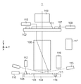
図1は、本発明の一側面としての露光装置1の構成を示す概略図である。露光装置1は、レチクル101を保持するレチクルステージ102と、基板103を保持する基板ステージ104と、レチクルステージ102に保持されたレチクル101を照明する照明光学系105とを有する。また、露光装置1は、レチクル101のパターン(の像)を基板ステージ104に保持された基板103に投影する投影光学系106と、露光装置1の全体の動作を統括的に制御する制御部117とを有する。
FIG. 1 is a schematic view showing a configuration of an
露光装置1は、本実施形態では、レチクル101と基板103とを走査方向に互いに同期走査しながら(即ち、ステップ・アンド・スキャン方式で)、レチクル101のパターンを基板103に転写する走査型露光装置(スキャナー)である。但し、露光装置1は、レチクル101を固定して(即ち、ステップ・アンド・リピート方式で)、レチクル101のパターンを基板103に転写する露光装置(ステッパー)であってもよい。
In this embodiment, the
以下では、投影光学系106の光軸と一致する方向をZ軸方向、Z軸方向に垂直な平面内でレチクル101及び基板103の走査方向をY軸方向、Z軸方向及びY軸方向に垂直な方向(非走査方向)をX軸方向とする。また、X軸回り、Y軸回り及びZ軸回りのそれぞれの方向を、θX方向、θY方向及びθZ方向とする。
In the following, the direction coincident with the optical axis of the projection
レチクルステージ102は、投影光学系106の光軸に垂直な平面内、即ち、XY平面内で2次元移動可能に、且つ、θZ方向に回転可能に構成される。但し、レチクルステージ102は、リニアモータなどの駆動装置によって1軸駆動又は6軸駆動される。
The
レチクルステージ102にはミラー107が配置され、ミラー107に対向する位置にはレーザ干渉計109が配置されている。レチクルステージ102の2次元方向の位置及び回転角はレーザ干渉計109によってリアルタイムで計測され、かかる計測結果は制御部117に出力される。制御部117は、レーザ干渉計109の計測結果に基づいて駆動装置を制御し、レチクルステージ102に保持されたレチクル101を位置決めする。
A
投影光学系106は、複数の光学素子を含み、レチクル101のパターンを所定の投影倍率βで基板103に投影する。投影光学系106は、本実施形態では、投影倍率βとして、例えば、1/4又は1/5を有する縮小光学系である。
The projection
基板ステージ104は、チャックを介して基板103を保持するZステージと、Zステージを支持するXYステージと、XYステージを支持するベースとを含む。基板ステージ104は、リニアモータなどの駆動装置によって駆動される。
The
基板ステージ104には、ミラー108が配置され、ミラー108に対向する位置にはレーザ干渉計110及び112が配置されている。基板ステージ104のX軸方向、Y軸方向及びθZ方向の位置はレーザ干渉計110によってリアルタイムで計測され、かかる計測結果は制御部117に出力される。同様に、基板ステージ104のZ軸方向の位置、θX方向及びθY方向の位置はレーザ干渉計112によってリアルタイムに計測され、かかる計測結果は制御部117に出力される。制御部117は、レーザ干渉計110及び112の計測結果に基づいて駆動装置を制御し、基板ステージ104に保持された基板103を位置決めする。
A
レチクルアライメント検出系113は、レチクルステージ102の近傍に配置される。レチクルアライメント検出系113は、レチクルステージ102に保持されたレチクル101の上のレチクル基準マークと、投影光学系106を介して基板ステージ104に配置されたステージ基準プレート111の上の基準マークMK1とを検出する。
The reticle
レチクルアライメント検出系113は、基板103を実際に露光する際に用いられる光源と同一の光源を用いて、レチクル101の上のレチクル基準マークと、投影光学系106を介して基準マークMK1とを照明する。また、レチクルアライメント検出系113は、レチクル基準マーク及び基準マークMK1からの反射光を撮像素子(例えば、CCDカメラなどの光電変換素子)で検出する。かかる撮像素子からの検出信号に基づいて、レチクル101と基板103との位置合わせ(アライメント)が行われる。この際、レチクル101の上のレチクル基準マークとステージ基準プレート111の上の基準マークMK1の位置及びフォーカスを合わせることで、レチクル101と基板103との相対的な位置関係(X、Y、Z)を合わせることができる。
The reticle
レチクルアライメント検出系114は、基板ステージ104に配置される。レチクルアライメント検出系114は、透過型の検出系であって、基準マークMK1が透過型のマークである場合に使用される。レチクルアライメント検出系114は、基板103を実際に露光する際に用いられる光源と同一の光源を用いて、レチクル101の上のレチクル基準マーク及び基準マークMK1を照明し、かかるマークからの透過光を光量センサで検出する。この際、レチクルアライメント検出系114は、基板ステージ104をX軸方向(又はY軸方向)及びZ軸方向に駆動させながら透過光の光量を検出する。これにより、レチクル101の上のレチクル基準マークとステージ基準プレート111の上の基準マークMK1との位置及びフォーカスを合わせることができる。
The reticle
このように、レチクルアライメント検出系113、或いは、レチクルアライメント検出系114のどちらを用いても、レチクル101と基板103との相対的な位置関係(X、Y、Z)を合わせることができる。
As described above, the relative positional relationship (X, Y, Z) between the
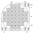
図2に示すように、ステージ基準プレート111は、基板103の表面とほぼ同じ高さになるように、基板ステージ104のコーナーに配置される。ステージ基準プレート111は、基板ステージ104の1つのコーナーに配置されていてもよいし、基板ステージ104の複数のコーナーに配置されていてもよい。
As shown in FIG. 2, the
ステージ基準プレート111は、レチクルアライメント検出系113又は114によって検出される基準マークMK1と、基板アライメント検出系116によって検出される基準マークMK2とを有する。ステージ基準プレート111は、複数の基準マークMK1や複数の基準マークMK2を有していてもよい。また、基準マークMK1と基準マークMK2との位置関係(X軸方向及びY軸方向)は、所定の位置関係に設定されている(即ち、既知である)。なお、基準マークMK1と基準マークMK2とは、共通のマークであってもよい。
The
フォーカス検出系115は、基板103の表面に光を投射する投射系と、基板103の表面で反射した光を受光する受光系とを含み、基板103のフォーカス(Z軸方向の位置)を検出し、かかる検出結果を制御部117に出力する。制御部117は、フォーカス検出系115の検出結果に基づいて基板ステージ104を駆動する駆動装置を制御し、基板ステージ104に保持された基板103のZ軸方向の位置及び傾斜角を調整する。
The
基板アライメント検出系116は、基板103の上のアライメントマークAM1やステージ基準プレート111の上の基準マークMK2を照明する照明系と、かかるマークからの光によりマークの像を形成する結像系とを含む。基板アライメント検出系116は、アライメントマークAM1や基準マークMK2の位置を検出し、かかる検出結果を制御部117に出力する。制御部117は、基板アライメント検出系116の検出結果に基づいて基板ステージ104を駆動する駆動装置を制御し、基板ステージ104に保持された基板103のX軸方向及びY軸方向の位置を調整する。
The substrate
なお、基板アライメント検出系の構成は、一般的には、オフアクシス(Off−axis)検出系とTTL−AA(Through the Lens Auto Alignment)検出系の2つに大別される。オフアクシス検出系は、投影光学系を介さずに、基板の上のアライメントマークを光学的に検出する。TTL−AA検出系は、投影光学系を介して、露光光の波長とは異なる波長の光を用いて基板の上のアライメントマークを検出する。基板アライメント検出系116は、本実施形態では、オフアクシス検出系であるが、TTL−AA検出系であってもよい。基板アライメント検出系116がTTL−AA検出系である場合には、投影光学系106を介して、基板103の上のアライメントマークAM1を検出するが、基本的な構成はオフアクシス検出系と同様である。
The configuration of the substrate alignment detection system is generally roughly divided into two types, an off-axis detection system and a TTL-AA (Through the Lens Auto Alignment) detection system. The off-axis detection system optically detects an alignment mark on the substrate without using a projection optical system. The TTL-AA detection system detects an alignment mark on the substrate using light having a wavelength different from the wavelength of exposure light via the projection optical system. The substrate
図3を参照して、基板アライメント検出系116について詳細に説明する。図3は、基板アライメント検出系116の具体的な構成を示す概略断面図である。基板アライメント検出系116は、上述したように、アライメントマークAM1や基準マークMK2などの被検体(の位置)を検出する検出装置として機能する。
The substrate
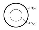
光源20は、基板103を透過しない可視光及び基板103を透過する赤外光を射出する光源である。光源20から射出された光は、第1リレー光学系21、波長フィルタ板22及び第2リレー光学系23を通過して、基板アライメント検出系116の瞳面(物体面に対する光学的なフーリエ変換面)に位置する開口絞り板24に到達する。なお、開口絞り板24でのビーム径LD24は、図4に示すように、光源20でのビーム径LD20よりも十分に小さくなる。図4は、光源20でのビーム径LD20と開口絞り板24でのビーム径LD24との関係を示す図である。
The
波長フィルタ板22には、透過させる光の波長帯域が互いに異なる複数のフィルタが配置され、制御部117の制御下において、複数のフィルタから1つのフィルタが選択されて基板アライメント検出系116の光路に配置される。換言すれば、波長フィルタ板22は、基板アライメント検出系116の光路に対して、互いに異なる透過率を有する複数のフィルタを交換可能に保持する。なお、波長フィルタ板22は、新たなフィルタを追加することが可能な構成を有する。図5は、基板103としてのSi基板の入射光の波長に対する透過率を模式的に示す図である。Si基板は、図5に示すように、波長1000nm程度から透過率が増加する特性を有している。従って、Si基板の裏面に形成されたアライメントマークは波長1000nm以上の光で検出することが可能であり、Si基板の表面に形成されたアライメントマークは波長1000nm未満の波長の光で検出することが可能である。そこで、本実施形態では、可視光を透過する可視光用のフィルタ及び赤外光を透過する赤外光用のフィルタを波長フィルタ板22に配置し、これらのフィルタを切り替えることで、可視光及び赤外光のいずれか一方の光でアライメントマークを照明する。また、波長フィルタ板22に配置されたフィルタを切り替えるのではなく、可視光を射出する可視光源と赤外光を射出する赤外光源とを準備して、それらの光源を切り替えることで、可視光及び赤外光のいずれか一方の光でアライメントマークを照明してもよい。
A plurality of filters having different wavelength bands of light to be transmitted are arranged on the
開口絞り板24には、互いに照明σが異なる複数の開口絞りが配置され、制御部117の制御下において、基板アライメント検出系116の光路に配置する開口絞りを切り替えることで、アライメントマークを照明する光の照明σを変更することができる。なお、開口絞り板24は、新たな開口絞りを追加することが可能な構成を有する。
A plurality of aperture stops having different illuminations σ are arranged on the
開口絞り板24に到達した光は、第1照明系25及び第2照明系27を介して、偏光ビームスプリッター28に導光される。偏光ビームスプリッター28に導光された光のうち紙面に垂直なS偏光は、偏光ビームスプリッター28で反射され、NA絞り26及びλ/4板29を透過して円偏光に変換される。λ/4板29を透過した光束は、対物レンズ30を通過して、基板103の表面に形成されたアライメントマークAM1を照明する。なお、NA絞り26は、制御部117の制御下において、絞り量を変えることでNAを変更することができる。
The light reaching the
アライメントマークAM1からの反射光、回折光及び散乱光は、対物レンズ30を通過し、λ/4板29を透過して紙面に平行なP偏光に変換され、NA絞り26を介して、偏光ビームスプリッター28を透過する。偏光ビームスプリッター28を透過した光は、リレーレンズ31、第1結像系32、コマ収差調整用光学部材35、第2結像光学系33及び波長シフト差調整用光学部材39を介して、撮像素子34の上にアライメントマークAM1の像を形成する。撮像素子34は、アライメントマークAM1の像を撮像して検出信号を出力する。
Reflected light, diffracted light, and scattered light from the
基板アライメント検出系116が基板103の上のアライメントマークAM1を検出する場合、アライメントマークAM1の上には、レジスト(透明層)が塗布(形成)されているため、単色光又は狭い波長帯域の光では干渉縞が発生してしまう。従って、撮像素子34からの検出信号(アライメント信号)に干渉縞の信号が加算され、アライメントマークAM1(の位置)を高精度に検出することができなくなる。そこで、一般的には、広帯域の波長の光を射出する光源を光源20として用いて、撮像素子34からの検出信号に干渉縞の信号が加算されることを低減している。
When the substrate
また、基板103の上のアライメントマークAM1を高精度に検出するためには、撮像素子34においてアライメントマークAM1の像を明確に撮像しなければならない。換言すれば、基板アライメント検出系116の焦点(ピント)がアライメントマークAM1に合っていなければならない。そこで、基板アライメント検出系116は、一般的には、AF検出系(不図示)を有し、かかるAF検出系の検出結果に基づいて、アライメントマークAM1をベストフォーカス面に位置させた状態でアライメントマークAM1を検出する。
Further, in order to detect the alignment mark AM1 on the
基板アライメント検出系116による基板103の裏面に形成されたアライメントマーク(被検体)AM2の検出について説明する。図6は、基板アライメント検出系116が基板103の表面に形成されたアライメントマークAM1及び基板103の裏面に形成されたアライメントマークAM2を検出している状態を示している。上述したように、基板103の表面に形成されたアライメントマークAM1を検出する場合には、図6(a)に示すように、可視光VLでアライメントマークAM1を照明する。一方、基板103の裏面に形成されたアライメントマークAM2を検出する場合には、図6(b)に示すように、赤外光ILでアライメントマークAM2を照明する。なお、基板103の表面にはレジストRSが塗布されているが、塗布むらなどによって、レジストRSの表面は平坦ではなく、凹凸が形成されている。
The detection of the alignment mark (subject) AM2 formed on the back surface of the
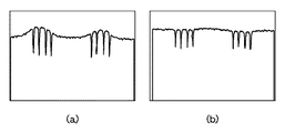
例えば、基板103の表面に形成されたアライメントマークAM1を狭い波長帯域の可視光(例えば、550nm〜580nmなどの波長帯域30nmの可視光)を用いて検出すると、図7(a)に示すような検出信号が得られる。図7(a)を参照するに、レジストRSの表面の凹凸の影響による干渉縞が発生しており、このような検出信号からは、上述したように、アライメントマークAM1(の位置)を高精度に検出することができない。
For example, when the alignment mark AM1 formed on the surface of the
一方、基板103の表面に形成されたアライメントマークAM1を広い波長帯域の可視光(例えば、500nm〜700nmなどの波長帯域200nmの可視光)を用いて検出すると、図7(b)に示すような検出信号が得られる。図7(b)に示す検出信号は、図7(a)に示す検出信号と比較して、干渉縞の影響が低減されている。
On the other hand, when the alignment mark AM1 formed on the surface of the
図8は、アライメントマークAM1を検出する際に用いた光の波長帯域とアライメントマークAM1の検出誤差(計測だまされ)との関係を示す図である。図8を参照するに、狭い波長帯域WBaの光を用いた場合には、検出誤差が十分に平均化されずに、真値からマイナス方向に検出誤差が生じてしまう。同様に、狭い波長帯域WBbの光を用いた場合にも、検出誤差が十分に平均化されずに、真値からプラス方向に検出誤差が生じてしまう。それに対して、広い波長帯域WBcの光を用いた場合には、検出誤差が平均化され、計測誤差が低減されて真値に近くなる。このように、アライメントマークを検出する際には、広い波長帯域の光を用いることで干渉縞の影響を低減し、アライメントマークを高精度に検出することができるという利点がある。但し、波長帯域を広げすぎると、平均化効果によって検出信号のコントラストが低下してしまう。従って、コントラストの低下が許容される範囲内において、波長帯域を広げる必要がある。 FIG. 8 is a diagram showing the relationship between the wavelength band of light used when detecting the alignment mark AM1 and the detection error (measurement trick) of the alignment mark AM1. Referring to FIG. 8, when light of a narrow wavelength band WBa is used, the detection error is not sufficiently averaged, and a detection error occurs in the minus direction from the true value. Similarly, when light of a narrow wavelength band WB b is used, the detection error is not sufficiently averaged, and a detection error occurs in the plus direction from the true value. On the other hand, when light of a wide wavelength band WB c is used, the detection error is averaged, the measurement error is reduced, and it becomes close to the true value. Thus, when detecting the alignment mark, there is an advantage that the influence of the interference fringes can be reduced by using light of a wide wavelength band, and the alignment mark can be detected with high accuracy. However, if the wavelength band is excessively widened, the contrast of the detection signal is lowered due to the averaging effect. Therefore, it is necessary to widen the wavelength band within a range in which a decrease in contrast is allowed.
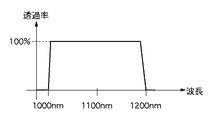
赤外光を用いて基板103の裏面に形成されたアライメントマークAM2を検出する場合について考える。基板103の波長に対する透過率は、図5に示す透過率であるものとする。図5を参照するに、波長1000nm以上の光が基板103を透過するため、アライメントマークAM2を検出する際には、波長1000nm以上の赤外光を用いる。一般的に、赤外光(波長帯域1000nm〜1200nm)に対する撮像素子34の感度は、図9に示すように、波長1000nmで最も高くなり、長波長側である1200nmに近づくにつれて低くなる。
Consider a case where the alignment mark AM2 formed on the back surface of the
基板103の裏面に形成されたアライメントマークAM2を波長1000nm〜1030nmなどの波長帯域30nmの赤外光(狭い波長帯域の赤外光)を用いて検出すると、干渉縞が発生し、図7(a)に示したような検出信号が得られる。そこで、干渉縞の影響を低減するために、基板103の裏面に形成されたアライメントマークAM2を波長1000nm〜1200nmなどの波長帯域200nmの赤外光(広い波長帯域の赤外光)を用いて検出しても、図7(a)に示したような検出信号が得られる。この際、波長フィルタ板22に配置された複数のフィルタから、図10に示すように、波長帯域1000nm〜1200nmに対してほぼ100%の透過率を有するフィルタが選択され、かかるフィルタが基板アライメント検出系116の光路に配置される。
When the alignment mark AM2 formed on the back surface of the
このように、広い波長帯域の赤外光を用いても、基板103の裏面に形成されたアライメントマークAM2を検出する場合には、図7(a)に示すようなアラ検出信号が得られてしまう。これは、図9に示したように、赤外光(波長帯域1000nm〜1200nm)に対する撮像素子34の感度が長波長側に近づくにつれて低くなることが原因である。図9を参照するに、1100nm〜1200nmの波長帯域では、1000nm〜1050nmの波長帯域に比べて撮像素子34の感度が低くなっている。従って、波長帯域1000nm〜1200nmの広い波長帯域の赤外光を用いても、実質的には、1000nm〜1050nm程度の狭い波長帯域の赤外光しか検出信号に現れない。換言すれば、広い波長帯域の赤外光を用いても、赤外光の波長帯域における撮像素子34の感度が均一ではないため、狭い波長帯域の赤外光しか検出信号に寄与せず、干渉縞の影響を十分に低減することができない。
As described above, when detecting the alignment mark AM2 formed on the back surface of the
そこで、本実施形態では、以下に説明するように、赤外光の波長帯域において、基板アライメント検出系116の光路における第1波長帯域の光に対する透過率と第1波長帯域とは異なる第2波長帯域の光に対する透過率とを異ならせる。これにより、撮像素子34で撮像されるアライメントマークAM2の像を形成する第1波長帯域の光の強度と撮像素子34で撮像されるアライメントマークAM2の像を形成する第2波長帯域の光の強度との強度差を低減する。換言すれば、本実施形態では、赤外光の波長帯域において、撮像素子34で撮像されるアライメントマークAM2の像を形成する光の強度を均一にする。
Therefore, in the present embodiment, as described below, in the wavelength band of infrared light, the transmittance for light in the first wavelength band in the optical path of the substrate
具体的には、赤外光の波長帯域1000nm〜1200nmにおいて、各波長帯域に対して異なる透過率(透過強度)を有するフィルタ(光学部材)を用いる。例えば、図11に示すように、撮像素子34の感度(図9参照)とは逆の透過率を有するフィルタを用いる。図11を参照するに、かかるフィルタでは、波長帯域1000nm〜1100nm(短波長側)での透過率が低く、波長帯域1100nm〜1200nm(長波長側)での透過率が高くなっている。換言すれば、かかるフィルタは、撮像素子34で撮像されるアライメントマークAM2の像を形成する短波長側の光の強度と長波長側の光の強度との強度差をゼロにするための透過率を有している。このようなフィルタを波長フィルタ板22に配置しておき、アライメントマークAM2を検出する際に基板アライメント検出系116の光路に配置する。
Specifically, a filter (optical member) having a different transmittance (transmission intensity) for each wavelength band in the infrared wavelength band of 1000 nm to 1200 nm is used. For example, as shown in FIG. 11, a filter having a transmittance opposite to the sensitivity of the image sensor 34 (see FIG. 9) is used. Referring to FIG. 11, in such a filter, the transmittance in the
図11に示す透過率を有するフィルタを基板アライメント検出系116の光路に配置して、基板103の裏面に形成されたアライメントマークAM2を検出する場合について説明する。図11に示す透過率を有するフィルタは、上述したように、波長帯域1000nm〜1100nmでの透過率が低く、波長帯域1100nm〜1200nmでの透過率が高くなっている。ここで、図9に示す撮像素子34の感度の波長依存性を含めて考えると、撮像素子34で撮像されるアライメントマークAM2の像を形成する光の波長帯域1000nm〜1200nmにおける強度が均一になる。従って、図11に示す透過率を有するフィルタを通過した波長帯域1000nm〜1200nmの赤外光を用いてアライメントマークAM2を検出すれば、図7(b)に示したような、干渉縞が十分に低減された検出信号を得ることができる。
A case where the filter having the transmittance shown in FIG. 11 is arranged in the optical path of the substrate
このように、本実施形態では、赤外光の波長帯域1000nm〜1200nmにおいて、図9に示す撮像素子34の感度の波長依存性とは逆の透過率(透過率分布)を有するフィルタを用いる。換言すれば、波長帯域1000nm〜1200nmにおいて、基板アライメント検出系116の波長帯域1000nm〜1100nmの光に対する透過率と波長帯域1100nm〜1200nmの光に対する透過率が異ならせる。これにより、基板アライメント検出系116において、波長帯域1000nm〜1200nmでの分光特性が均一になり、干渉縞の影響が低減された検出信号を得ることができるため、アライメントマークAM2(の位置)を高精度に検出することができる。
As described above, in the present embodiment, a filter having a transmittance (transmittance distribution) opposite to the wavelength dependency of the sensitivity of the
一方、従来技術では、上述したように、図10に示す透過率を有するフィルタを通過した波長帯域1000nm〜1200nmの赤外光を用いてアライメントマークAM2を検出している。この場合、撮像素子34の感度の波長依存性によって、図7(a)に示したような検出信号しか得ることができない。
On the other hand, in the prior art, as described above, alignment mark AM2 is detected using infrared light having a wavelength band of 1000 nm to 1200 nm that has passed through the filter having the transmittance shown in FIG. In this case, only the detection signal as shown in FIG. 7A can be obtained due to the wavelength dependence of the sensitivity of the
本実施形態では、赤外光の波長帯域1000nm〜1200nmにおいて、各波長帯域に対して異なる透過率を有する光学部材としてフィルタを用いたが、このような透過率を有するのであれば、フィルタ以外の光学部材を用いてもよい。また、光源側において各波長帯域の光の光量を制御してもよい。例えば、互いに異なる波長帯域の光を射出する複数の光源(光学部)を用いて、それぞれの光源から射出される光の光量(即ち、基板アライメント検出系に入射する光の各波長帯域における光量)を調整することで、各波長帯域の光の光量を制御することができる。また、ハロゲンランプを光源として用いている場合には、ハロゲンランプに供給する電圧(供給電圧)を調整することで各波長帯域の光の光量を制御することも可能である。例えば、ハロゲンランプは、供給電圧を高くすると、短波長側の光の強度が長波長側の光の強度よりも高くなる傾向を有する。従って、短波長側の光に対する透過率を長波長側の光に対する透過率よりも高くしたい場合には、供給電圧を高くすればよい。一方、短波長側の光に対する透過率を長波長側の光に対する透過率よりも低くしたい場合には、供給電圧を低くすればよい。 In the present embodiment, a filter is used as an optical member having a different transmittance for each wavelength band in the wavelength band of 1000 nm to 1200 nm of infrared light. An optical member may be used. Further, the light quantity of each wavelength band may be controlled on the light source side. For example, by using a plurality of light sources (optical units) that emit light in different wavelength bands, the amount of light emitted from each light source (that is, the amount of light in each wavelength band of light incident on the substrate alignment detection system) The amount of light in each wavelength band can be controlled by adjusting. When a halogen lamp is used as a light source, the amount of light in each wavelength band can be controlled by adjusting the voltage (supply voltage) supplied to the halogen lamp. For example, in a halogen lamp, when the supply voltage is increased, the intensity of light on the short wavelength side tends to be higher than the intensity of light on the long wavelength side. Accordingly, when it is desired to make the transmittance for light on the short wavelength side higher than the transmittance for light on the long wavelength side, the supply voltage may be increased. On the other hand, when it is desired to make the transmittance for light on the short wavelength side lower than the transmittance for light on the long wavelength side, the supply voltage may be lowered.
本実施形態では、赤外光の波長帯域1000nm〜1200nmを例に説明したが、波長帯域を限定するものではなく、干渉縞が十分に低減されれば、波長帯域は1050nm〜1200nmや1100nm〜1250nmであってもよい。また、本実施形態は、赤外光の波長帯域1000nm〜1200nmにおける撮像素子の感度の波長依存性を例に説明したが、赤外光の波長帯域以外、例えば、可視光の波長領域における撮像素子の感度の波長依存性にも適用可能である。 In the present embodiment, the wavelength band of infrared light has been described as an example of 1000 nm to 1200 nm, but the wavelength band is not limited, and if the interference fringes are sufficiently reduced, the wavelength band is 1050 nm to 1200 nm or 1100 nm to 1250 nm. It may be. Moreover, although this embodiment demonstrated the wavelength dependence of the sensitivity of the image pick-up element in the wavelength range of 1000 nm-1200 nm of infrared light as an example, for example, in the wavelength range of visible light other than the wavelength band of infrared light It is also applicable to the wavelength dependence of the sensitivity.
次に、基板103のプロセスが検出信号に与える影響について説明する。図12(a)に示すように、基板103の上にレジストRSaが塗布されている場合、及び、図12(b)に示すように、基板103の上に層間膜LC及びレジストRSbが塗布されている場合について考える。図12(a)及び図12(b)を参照するに、基板103に塗布されたレジストRSa及びRSbの表面は平坦ではなく、塗布むらなどによって、凹凸が形成されているため、広い波長帯域の光を用いて干渉縞を低減する必要がある。図12(a)及び図12(b)のそれぞれについて、図10に示したような波長帯域1000nm〜1200nmに対してほぼ100%の透過率を有するフィルタを基板アライメント検出系116の光路に配置した場合を考える。この場合、波長帯域1000nm〜1200nmの赤外光を用いてアライメントマークAM2を検出すると、図7(a)に示したような検出信号しか得ることができない。
Next, the influence of the process of the
そこで、図12(a)及び図12(b)のそれぞれについて、図11に示す透過率を有するフィルタを基板アライメント検出系116の光路に配置して、基板103の裏面に形成されたアライメントマークAM2を検出する場合について考える。この場合、上述したように、図7(b)に示したような、干渉縞が十分に低減された検出信号が得られることが期待されるが、実際には、図7(a)に示したような検出信号が得られてしまう。図6では、基板103のプロセス自体の波長に対する分光特性がほぼ均一であったため、撮像素子34の感度の波長依存性を逆補正するフィルタ(図11参照)を用いることで、基板アライメント検出系116の分光特性を均一にすることができる。但し、図12(a)及び図12(b)では、基板103のプロセス自体の波長に対する分光特性が均一でないため、撮像素子34の感度の波長依存性を逆補正するフィルタを用いるだけでは、基板アライメント検出系116の分光特性を均一にすることができない。このような場合には、撮像素子34の感度の波長依存性だけではなく、基板103のプロセス自体の波長に対する分光特性も考慮して、基板アライメント検出系116の分光特性を均一にする必要がある。
Therefore, in each of FIGS. 12A and 12B, a filter having the transmittance shown in FIG. 11 is arranged in the optical path of the substrate
そこで、以下では、撮像素子34の感度の波長依存性だけではなく、基板103のプロセス自体の波長に対する分光特性も考慮して、基板アライメント検出系116の分光特性を均一にすることについて説明する。
Therefore, in the following, description will be given of making the spectral characteristics of the substrate
図12(a)に示す基板103のプロセスについて考える。まず、図13(a)に示すような透過率を有するフィルタを基板アライメント検出系116の光路に配置して、図12(a)に示す基板103の裏面に形成されたアライメントマークAM2を検出する。図13(a)に示す透過率を有するフィルタは、波長帯域1000nm〜1100nmでの透過率がほぼ100%、波長帯域1100nm〜1200nmでの透過率が0%となっている。この場合、アライメントマークAM2を照明する赤外光の波長帯域は1000nm〜1100nmとなり、十分に広い波長帯域の赤外光ではないため、図7(a)に示したような干渉縞が低減されていない検出信号が得られる。この際、撮像素子34で撮像されるアライメントマークAM2の像を形成する光(検出信号)の強度が80%であったとする。
Consider the process of the
次に、図13(b)に示すような透過率を有するフィルタを基板アライメント検出系116の光路に配置して、図12(a)に示す基板103の裏面に形成されたアライメントマークAM2を検出する。図13(b)に示す透過率を有するフィルタは、波長帯域1100nm〜1200nmでの透過率がほぼ100%、波長帯域1000nm〜1100nmでの透過率が0%となっている。この場合、アライメントマークAM2を照明する赤外光の波長帯域は1100nm〜1200nmとなり、十分に広い波長帯域の赤外光ではないため、図7(a)に示したような干渉縞が低減されていない検出信号が得られる。この際、撮像素子34で撮像されるアライメントマークAM2の像を形成する光の強度が4%であったとする。なお、フィルタ以外の検出信号(特に、強度)に影響を与える他の条件(アライメントマークAM2を検出する際の条件、例えば、光源20の電圧、撮像素子34の蓄積時間)は変更しないものとする。
Next, a filter having transmittance as shown in FIG. 13B is arranged in the optical path of the substrate
このように、赤外光の波長帯域に対して互いに異なる透過率を有する2つのフィルタを用いてアライメントマークAM2を検出することで、撮像素子34で撮像されるアライメントマークAM2の像を形成する光(検出信号)の強度に20倍の差が生じている。これは、波長帯域1000nm〜1100nmと波長帯域1100nm〜1200nmとでの、撮像素子34の感度の波長依存性に基板103のプロセス自体の波長に対する分光特性を考慮した場合の基板アライメント検出系116の分光特性の差を示している。
In this way, light that forms an image of the alignment mark AM2 imaged by the
そこで、本実施形態では、図13(c)に示す透過率を有するフィルタを用いて、波長帯域1000nm〜1200nmにおける20倍の強度比を補正する。図13(c)に示す透過率を有するフィルタは、波長帯域1100nm〜1200nmでの透過率がほぼ100%、波長帯域1000nm〜1100nmでの透過率がほぼ5%になっている。従って、波長帯域1000nm〜1100nmでの透過率と波長帯域1100nm〜1200nmでの透過率との比が1:20になっている。換言すれば、図13(c)に示すフィルタの透過率は、波長帯域1000nm〜1100での強度(80%)と波長帯域1100nm〜1200nmでの強度(4%)との比と逆の関係になっている。図13(c)に示す透過率を有するフィルタを通過した波長帯域1000nm〜1200nmの赤外光を用いてアライメントマークAM2を検出すれば、図7(b)に示したような、干渉縞が十分に低減された検出信号を得ることができる。
Therefore, in the present embodiment, a 20-fold intensity ratio in the wavelength band of 1000 nm to 1200 nm is corrected using a filter having the transmittance shown in FIG. The filter having the transmittance shown in FIG. 13C has a transmittance of approximately 100% in the wavelength band of 1100 nm to 1200 nm, and a transmittance of approximately 5% in the wavelength band of 1000 nm to 1100 nm. Therefore, the ratio of the transmittance in the
図12(b)に示す基板103のプロセスについて考える。図13(c)に示すような透過率を有するフィルタを基板アライメント検出系116の光路に配置して、図12(b)に示す基板103の裏面に形成されたアライメントマークAM2を検出する。この場合、図7(a)に示したような干渉縞が低減されていない検出信号が得られる。これは、図12(b)に示す基板103のプロセスは図12(a)に示す基板103のプロセスと異なり、基板103のプロセスの波長に対する分光特性が異なるためである。
Consider the process of the
そこで、まず、図13(a)に示すような透過率を有するフィルタを基板アライメント検出系116の光路に配置して、図12(b)に示す基板103の裏面に形成されたアライメントマークAM2を検出する。この場合、アライメントマークAM2を照明する赤外光の波長帯域は1000nm〜1100nmとなり、十分に広い波長帯域の赤外光ではないため、図7(a)に示したような干渉縞が低減されていない検出信号が得られる。この際、撮像素子34で撮像されるアライメントマークAM2の像を形成する光(検出信号)の強度が70%であったとする。
Therefore, first, a filter having transmittance as shown in FIG. 13A is arranged in the optical path of the substrate
次に、図13(b)に示すような透過率を有するフィルタを基板アライメント検出系116の光路に配置して、図12(b)に示す基板103の裏面に形成されたアライメントマークAM2を検出する。この場合、アライメントマークAM2を照明する赤外光の波長帯域は1100nm〜1200nmとなり、十分に広い波長帯域の赤外光ではないため、図7(a)に示したような干渉縞が低減されていない検出信号が得られる。この際、撮像素子34で撮像されるアライメントマークAM2の像を形成する光の強度が35%であったとする。なお、フィルタ以外の検出信号(特に、強度)に影響を与える他の条件(アライメントマークAM2を検出する際の条件、例えば、光源20の電圧、撮像素子34の蓄積時間)は変更しないものとする。
Next, a filter having transmittance as shown in FIG. 13B is arranged in the optical path of the substrate
このように、赤外光の波長帯域に対して互いに異なる透過率を有する2つのフィルタを用いてアライメントマークAM2を検出することで、撮像素子34で撮像されるアライメントマークAM2の像を形成する光(検出信号)の強度に2倍の差が生じている。これは、波長帯域1000nm〜1100nmと波長帯域1100nm〜1200nmとでの、撮像素子34の感度の波長依存性に基板103のプロセス自体の波長に対する分光特性を考慮した場合の基板アライメント検出系116の分光特性の差を示している。
In this way, light that forms an image of the alignment mark AM2 imaged by the
そこで、本実施形態では、図13(d)に示す透過率を有するフィルタを用いて、波長帯域1000nm〜1200nmにおける2倍の強度比を補正する。図13(d)に示す透過率を有するフィルタは、波長帯域1100nm〜1200nmでの透過率がほぼ100%、波長帯域1000nm〜1100nmでの透過率がほぼ50%になっている。従って、波長帯域1000nm〜1100nmでの透過率と波長帯域1100nm〜1200nmでの透過率との比が1:2になっている。換言すれば、図13(d)に示すフィルタの透過率は、波長帯域1000nm〜1100での強度(70%)と波長帯域1100nm〜1200nmでの強度(35%)との比と逆の関係になっている。図13(d)に示す透過率を有するフィルタを通過した波長帯域1000nm〜1200nmの赤外光を用いてアライメントマークAM2を検出すれば、図7(b)に示したような、干渉縞が十分に低減された検出信号を得ることができる。
Therefore, in the present embodiment, a double intensity ratio in the wavelength band of 1000 nm to 1200 nm is corrected using a filter having the transmittance shown in FIG. In the filter having the transmittance shown in FIG. 13D, the transmittance in the
図14は、図12(a)及び図12(b)のそれぞれに示す基板103のプロセスについて、撮像素子34で撮像されるアライメントマークAM2の像を形成する光(検出信号)の強度とフィルタの透過率との関係を示す図である。図14を参照するに、フィルタの透過率比は、波長帯域1000nm〜1100nmと波長帯域1100nm〜1200nmとにおける強度比と逆となっていることがわかる。
FIG. 14 shows the intensity of the light (detection signal) and the filter forming the image of the alignment mark AM2 imaged by the
このように、本実施形態では、撮像素子34の感度の波長依存性だけではなく、基板103のプロセス自体の波長に対する分光特性も考慮して、基板アライメント検出系116の分光特性を均一にすることができる。
As described above, in this embodiment, the spectral characteristics of the substrate
なお、本実施形態では、図13(c)に示す透過率を有するフィルタ及び図13(d)に示す透過率を有するフィルタのそれぞれを波長フィルタ板22に配置して、基板103のプロセスに応じて切り替えることを想定している。但し、波長フィルタ板22には、波長帯域1000nm〜1100nmの光に対する透過率と波長帯域1100nm〜1200nmの光に対する透過率との比が1:5や1:10となる透過率を有するフィルタを配置しておいてもよい。
In the present embodiment, the filter having the transmittance shown in FIG. 13C and the filter having the transmittance shown in FIG. Switching. However, the
また、例えば、波長帯域1000nm〜1100nmと波長帯域1100nm〜1200nmとにおける強度比に対応する透過率比を有するフィルタが波長フィルタ板22に配置されていない場合もある。例えば、波長帯域1000nm〜1100nmと波長帯域1100nm〜1200nmとにおける強度比が6:1である場合を考える。そして、波長帯域1000nm〜1100nmの光に対する透過率と波長帯域1100nm〜1200nmの光に対する透過率との比が1:6となる透過率を有するフィルタが波長フィルタ板22に配置されていないとする。このような場合には、波長フィルタ板22に配置された複数のフィルタから、1:6の透過率比に最も近い透過率比、例えば、1:5の透過率比を有するフィルタを選択すればよい。
Further, for example, a filter having a transmittance ratio corresponding to the intensity ratio in the wavelength band of 1000 nm to 1100 nm and the wavelength band of 1100 nm to 1200 nm may not be disposed on the
また、基板103のプロセスに対して最適なフィルタを選択した場合には、基板103のプロセスと選択したフィルタとの対応関係を記憶部(例えば、制御部117のメモリなど)に記憶させてもよい。ここで、最適なフィルタとは、撮像素子34で撮像されるアライメントマークAM2の像を形成する短波長側の光の強度と長波長側の光の強度との強度差をゼロにするための透過率を有するフィルタである。これにより、同じプロセスの基板103の裏面に形成されたアライメントマークAM2を検出する場合には、記憶部に記憶された対応関係に基づいて、基板アライメント検出系116の光路に配置すべきフィルタを選択することができる。なお、基板アライメント検出系116の光路に配置すべきフィルタを選択した場合に限らず、基板103のプロセス(即ち、赤外線の波長帯域における強度比)と最適なフィルタとの対応関係を予め記憶部に記憶させておいてもよい。
In addition, when an optimum filter is selected for the process of the
また、本実施形態では、赤外光の波長帯域を1000nm〜1100nmの波長帯域及び1100nm〜1200nmの波長帯域の2つの波長帯域(2つの分割波長帯域)に分割したが、3つ以上の波長帯域に分割してもよい。例えば、赤外光の波長帯域1000nm〜1200nmを、波長帯域1000nm〜1060nm、波長帯域1060nm〜1130nm、波長帯域1130〜1200の3つの分割波長帯域に分割する。そして、それぞれの分割波長帯域での透過率がほぼ100%となる透過率を有するフィルタを基板アライメント検出系116の光路に配置してアライメントマークAM2を検出し、3つの分割波長帯域における強度比を求める。このように、赤外光の波長帯域に対して分割する波長帯域の数(分割波長帯域の数)は2つ以上であれば、3つであっても4つであってもよい。
Further, in this embodiment, the wavelength band of infrared light is divided into two wavelength bands (two divided wavelength bands) of a wavelength band of 1000 nm to 1100 nm and a wavelength band of 1100 nm to 1200 nm. You may divide into. For example, an infrared light wavelength band of 1000 nm to 1200 nm is divided into three divided wavelength bands, which are a wavelength band of 1000 nm to 1060 nm, a wavelength band of 1060 nm to 1130 nm, and a wavelength band of 1130 to 1200. Then, a filter having a transmittance of approximately 100% in each divided wavelength band is disposed in the optical path of the substrate
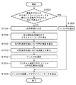
図15を参照して、露光装置1における基板アライメント検出系116の検出処理について説明する。かかる検出処理は、制御部117が露光装置1の各部、特に、基板アライメント検出系116の各部を統括的に制御することで行われる。ここでは、処理対象としての基板103のプロセスが以前にアライメントマークAM2を検出した基板のプロセスと同じである場合には、制御部117のメモリなどの記憶部に基板103のプロセスとフィルタとの対応関係が記憶されているものとする。また、基板アライメント検出系116は、動作モードとして、アライメントマークAM2の位置の検出を行う検出モードと、アライメントマークAM2の位置を検出するための準備を行う準備モードとを有するが、ここでは、準備モードについて詳細に説明する。なお、検出モードは、S1502、S1503及びS1516を含み、準備モードは、S1504乃至S1514を含む。
With reference to FIG. 15, the detection process of the substrate
S1502では、処理対象としての基板103のプロセスが以前にアライメントマークAM2を検出した基板のプロセスと同じであるかどうかを判定する。基板103のプロセスが以前にアライメントマークAM2を検出した基板のプロセスと同じである場合には、S1503に移行する。また、基板103のプロセスが以前にアライメントマークAM2を検出した基板のプロセスと同じでない場合には、S1504に移行する。
In S1502, it is determined whether or not the process of the
S1503では、記憶部に記憶されている基板103のプロセスとフィルタとの対応関係に基づいて、基板アライメント検出系116の光路に配置するフィルタを選択する。
In S1503, a filter to be arranged in the optical path of the substrate
S1504では、基板103の裏面に形成されたアライメントマークAM2を検出する際に用いる赤外線の波長帯域を決定する。具体的には、図7(b)に示したような、干渉縞が十分に低減された検出信号を得ることができるように、十分に広い波長帯域(例えば、波長帯域1000nm〜1200nm)を決定する。
In S1504, an infrared wavelength band used when detecting the alignment mark AM2 formed on the back surface of the
S1506では、S1504で決定された波長帯域を複数の分割波長帯域に分割し、各分割波長帯域の光でアライメントマークAM2を検出する。具体的には、各分割波長帯域での透過率がほぼ100%となる透過率を有するフィルタのそれぞれを基板アライメント検出系116の光路に配置してアライメントマークAM2を検出する。このようにして、アライメントマークAM2の検出は、分割波長帯域の数だけ繰り返される。
In S1506, the wavelength band determined in S1504 is divided into a plurality of divided wavelength bands, and the alignment mark AM2 is detected with light in each divided wavelength band. Specifically, the alignment mark AM2 is detected by disposing each filter having a transmittance of approximately 100% in each divided wavelength band in the optical path of the substrate
S1508では、S1506での検出結果に基づいて、各分割波長帯域について、撮像素子34で撮像されるアライメントマークAM2の像を形成する光の強度を算出する。例えば、波長帯域1000nm〜1200nmを波長帯域1000nm〜1100nmと波長帯域1100nm〜1200nmに分割した場合には、波長帯域1000nm〜1100nmでの強度と波長帯域1100nm〜1200nmでの強度を算出する。従って、撮像素子34で撮像されるアライメントマークAM2の像を形成する光の強度は、分割波長帯域の数だけ算出される。
In S1508, based on the detection result in S1506, the intensity of light forming the image of the alignment mark AM2 imaged by the
S1510では、S1508での算出結果に基づいて、S1504で決定した波長帯域における強度比を算出する。ここでは、波長帯域1000nm〜1100nmと波長帯域1100nm〜1200nmでの強度の比(強度比)が10:1であったものとする。
In S1510, the intensity ratio in the wavelength band determined in S1504 is calculated based on the calculation result in S1508. Here, it is assumed that the intensity ratio (intensity ratio) in the
S1512では、波長フィルタ板22に配置された複数のフィルタから、基板アライメント検出系116の光路に配置するフィルタを選択する。具体的には、S1510で算出した強度比に基づいて、撮像素子34で撮像されるアライメントマークAM2の像を形成する短波長側の光の強度と長波長側の光の強度との強度差を低減する透過率を有するフィルタを選択する。ここでは、波長帯域1000nm〜1100nmの光に対する透過率と波長帯域1100nm〜1200nmの光に対する透過率との比が1:10となる透過率を有するフィルタを選択する。但し、このような透過率を有するフィルタが波長フィルタ板22に配置されていない場合には、波長フィルタ板22に配置された複数のフィルタから、透過率の比が1:10に最も近い透過率を有するフィルタを選択する。
In S <b> 1512, a filter to be arranged in the optical path of the substrate
S1514では、基板103のプロセスとS1512で選択したフィルタとの対応関係を制御部117のメモリなどの記憶部に記憶する。
In S1514, the correspondence relationship between the process of the
S1516では、S1503又はS1512で選択したフィルタを基板アライメント検出系116の光路に配置し、基板103の裏面に形成されたアライメントマークAMを検出する。
In S1516, the filter selected in S1503 or S1512 is arranged in the optical path of the substrate
本実施形態の基板アライメント検出系116の検出処理によれば、干渉縞の影響が低減された検出信号を得ることができるため、基板103の裏面に形成されたアライメントマークAM2(の位置)を高精度に検出することができる。
According to the detection processing of the substrate
露光装置1による露光処理について説明する。光源から発せられた光は、照明光学系105を介して、レチクル101を照明する。レチクル101を通過してパターンを反映する光は、投影光学系106を介して、基板103に結像される。この際、基板103は、基板アライメント検出系116の検出結果に基づいて、高精度に位置決めされている。従って、露光装置1は、高いスループットで経済性よく高品位なデバイス(半導体集積回路素子、液晶表示素子等)を提供することができる。なお、デバイスは、露光装置1を用いてフォトレジスト(感光剤)が塗布された基板(ウエハ、ガラスプレート等)を露光する工程と、露光された基板を現像する工程と、その他の周知の工程と、を経ることにより製造される。
An exposure process performed by the
以上、本発明の好ましい実施形態について説明したが、本発明はこれらの実施形態に限定されないことはいうまでもなく、その要旨の範囲内で種々の変形及び変更が可能である。例えば、本実施形態では、赤外光を用いて基板の裏面に形成されたアライメントマークを検出する場合について説明したが、本発明は、可視光を用いて基板の表面に形成されたアライメントマークを検出する場合にも適用することができる。また、本実施形態では、基板アライメント検出系について説明したが、本発明は、レチクルアライメント検出系などの他の検出系にも適用することができる。更に、本発明は、オフアクシス検出系だけではなく、TTL−AA検出系にも適用することができる。 As mentioned above, although preferable embodiment of this invention was described, it cannot be overemphasized that this invention is not limited to these embodiment, A various deformation | transformation and change are possible within the range of the summary. For example, in the present embodiment, the case where the alignment mark formed on the back surface of the substrate is detected using infrared light has been described. However, the present invention uses the alignment mark formed on the surface of the substrate using visible light. It can also be applied to the case of detection. In the present embodiment, the substrate alignment detection system has been described. However, the present invention can also be applied to other detection systems such as a reticle alignment detection system. Furthermore, the present invention can be applied not only to an off-axis detection system but also to a TTL-AA detection system.
本発明は、被検体の位置を検出する検出装置、露光装置、デバイス製造方法及びフィルタに関する。 The present invention relates to a detection apparatus, an exposure apparatus , a device manufacturing method, and a filter that detect the position of a subject.
上記目的を達成するために、本発明の一側面としての検出装置は、被検体を検出する検出装置であって、前記被検体を第1波長帯域及び前記第1波長帯域とは異なる第2波長帯域を含む光で照明する照明系と、前記照明系により照明された前記被検体からの光を検出する検出器と、前記検出器で検出される前記第1波長帯域の光の強度値と前記第2波長帯域の光の強度値との差を低減する光学部材と、を有し、前記光学部材は、前記第1波長帯域の光の透過率と前記第2波長帯域の光の透過率とを異ならせることを特徴とする。
また、本発明の別の側面としてのフィルタは、被検体を赤外光で照明して前記被検体からの光を検出する検出装置に使用されるフィルタであって、前記赤外光のうち第1波長帯域の光の透過率と、前記赤外光のうち前記第1波長帯域とは異なる第2波長帯域の光の透過率とを異ならせることで、前記検出装置で検出される前記第1波長帯域の光の強度値と前記第2波長帯域の光の強度値との差を低減することを特徴とする。
To achieve the above object, the detection apparatus according to one aspect of the present invention is a detection device for detecting a test body, wherein the different second from the subject first wavelength band and said first wavelength band an illumination system for illuminating with light including a wavelength band, the intensity of the light detector and, before Symbol before Symbol first wavelength band that will be detected by a detector for detecting light from the subject illuminated by the illumination system possess an optical member for reducing the difference between the intensity values of the light values and the previous SL second wavelength band, and the optical member, wherein the light transmittance of the first wavelength band second wavelength band of light It is characterized in that the transmittance is different .
A filter according to another aspect of the present invention is a filter used in a detection device that detects light from the subject by illuminating the subject with infrared light, and includes a first of the infrared lights. By changing the transmittance of light in one wavelength band and the transmittance of light in a second wavelength band different from the first wavelength band in the infrared light, the first detected by the detection device The difference between the intensity value of the light in the wavelength band and the intensity value of the light in the second wavelength band is reduced.
本発明は、被検体の位置を検出する検出装置、露光装置、および、デバイスの製造方法に関する。 The present invention, detecting device for detecting the position of the object, an exposure apparatus, and relates to a device manufacturing method.
本発明の1つの側面に係る検出装置は、基板の裏面側に形成された被検体を赤外光を用いて検出する検出装置であって、第1波長帯域と前記第1波長帯域よりも長波長側の第2波長帯域とを含む赤外光で前記被検体を照明する照明系と、前記照明系により照明された前記被検体からの前記赤外光を検出する撮像素子であって、可視光、前記第1波長帯域の赤外光および前記第2波長帯域の赤外光に対する感度を有し、前記第1波長帯域の赤外光に対する感度よりも前記第2波長帯域の赤外光に対する感度が小さい撮像素子と、前記撮像素子の前記感度の差によって生じる、前記撮像素子で検出される前記第1波長帯域の赤外光の強度値と前記第2波長帯域の赤外光の強度値との差を、低減する光学部と、を有し、前記光学部は、前記第1波長帯域の赤外光と前記第2波長帯域の赤外光とで互いに異なる透過率を有することによって前記強度値の差を低減する光学部材、または、前記照明系に入射させる前記第1波長帯域の赤外光の光量と前記第2波長帯域の赤外光の光量とを異ならせることによって前記強度値の差を低減する光源装置であることを特徴とする。A detection apparatus according to one aspect of the present invention is a detection apparatus that detects an object formed on a back surface side of a substrate using infrared light, and has a first wavelength band and longer than the first wavelength band. An illumination system that illuminates the subject with infrared light including a second wavelength band on the wavelength side, and an imaging device that detects the infrared light from the subject illuminated by the illumination system, Light, sensitivity to infrared light in the first wavelength band and infrared light in the second wavelength band, and sensitivity to infrared light in the second wavelength band rather than sensitivity to infrared light in the first wavelength band. An intensity value of the infrared light in the first wavelength band and an intensity value of the infrared light in the second wavelength band detected by the image sensor, which is caused by a difference in sensitivity between the image sensor having a low sensitivity and the image sensor. And an optical unit that reduces the difference between the first wavelength and the optical unit An optical member that reduces the difference in intensity value by having different transmittance between infrared light in the region and infrared light in the second wavelength band, or in the first wavelength band that is incident on the illumination system The light source device is characterized in that the difference in intensity value is reduced by making the amount of infrared light different from the amount of infrared light in the second wavelength band.
Claims (9)
前記被検体を第1波長帯域及び前記第1波長帯域とは異なる第2波長帯域を含む光で照明する照明系と、
前記被検体からの光により前記被検体の像を形成する結像系と、
前記被検体の像を撮像する撮像素子と、
前記照明系又は前記結像系の光路における前記第1波長帯域の光に対する透過率と前記第2波長帯域の光に対する透過率とを異ならせることで、前記撮像素子で撮像される前記被検体の像を形成する前記第1波長帯域の光の強度と前記撮像素子で撮像される前記被検体の像を形成する前記第2波長帯域の光の強度との強度差を低減する光学部材と、
を有することを特徴とする検出装置。 A detection device for detecting the position of a subject,
An illumination system that illuminates the subject with light including a first wavelength band and a second wavelength band different from the first wavelength band;
An imaging system for forming an image of the subject by light from the subject;
An image sensor for capturing an image of the subject;
By varying the transmittance for the light in the first wavelength band and the transmittance for the light in the second wavelength band in the optical path of the illumination system or the imaging system, the object to be imaged by the imaging element is changed. An optical member that reduces an intensity difference between the intensity of light in the first wavelength band that forms an image and the intensity of light in the second wavelength band that forms an image of the subject imaged by the imaging device;
A detection apparatus comprising:
前記準備モードにおいて、
前記照明系は、前記第1波長帯域及び前記第2波長帯域を含む波長帯域を分割した複数の分割波長帯域の光のそれぞれで前記被検体を照明し、
前記撮像素子は、前記複数の分割波長帯域の光のそれぞれにより形成される前記被検体の像を撮像し、
前記光学部材は、互いに異なる透過率を有して前記光路に交換可能に配置される複数の光学素子を含み、
前記検出装置は、
前記撮像素子で撮像された前記複数の分割波長帯域の光のそれぞれにより形成される前記被検体の像の強度から前記波長帯域における強度比を求め、前記強度比に基づいて、前記複数の光学素子から前記強度差を低減する光学素子を選択し、前記選択した光学素子を前記検出モードにおいて前記光路に配置する制御部を更に有することを特徴とする請求項1に記載の検出装置。 The detection apparatus has, as operation modes, a detection mode for detecting the position of the subject, and a preparation mode for preparing for detecting the position of the subject,
In the preparation mode,
The illumination system illuminates the subject with each of a plurality of divided wavelength bands obtained by dividing a wavelength band including the first wavelength band and the second wavelength band,
The imaging device captures an image of the subject formed by each of the light of the plurality of divided wavelength bands,
The optical member includes a plurality of optical elements that have different transmittances and are arranged in the optical path in a replaceable manner.
The detection device includes:
An intensity ratio in the wavelength band is obtained from the intensity of the image of the subject formed by each of the light of the plurality of divided wavelength bands imaged by the imaging element, and the plurality of optical elements is based on the intensity ratio The detection apparatus according to claim 1, further comprising: a control unit that selects an optical element that reduces the intensity difference from the optical element and places the selected optical element in the optical path in the detection mode.
前記第1波長帯域及び前記第2波長帯域を含む光は、赤外光であることを特徴とする請求項1乃至5のうちいずれか1項に記載の検出装置。 The object is a mark formed on the back surface of the substrate,
The detection device according to claim 1, wherein the light including the first wavelength band and the second wavelength band is infrared light.
前記被検体を第1波長帯域及び前記第1波長帯域とは異なる第2波長帯域を含む光で照明する照明系と、
前記被検体からの光により前記被検体の像を形成する結像系と、
前記被検体の像を撮像する撮像素子と、
前記照明系に入射させる前記第1波長帯域の光の光量と前記第2波長帯域の光の光量とを異ならせることで、前記撮像素子で撮像される前記被検体の像を形成する前記第1波長帯域の光の強度と前記撮像素子で撮像される前記被検体の像を形成する前記第2波長帯域の光の強度との強度差を低減する光学部と、
を有することを特徴とする検出装置。 A detection device for detecting the position of a subject,
An illumination system that illuminates the subject with light including a first wavelength band and a second wavelength band different from the first wavelength band;
An imaging system for forming an image of the subject by light from the subject;
An image sensor for capturing an image of the subject;
The first light that forms an image of the subject to be imaged by the image sensor by making the amount of light of the first wavelength band incident on the illumination system different from the amount of light of the second wavelength band. An optical unit that reduces an intensity difference between the intensity of light in a wavelength band and the intensity of light in the second wavelength band that forms an image of the subject imaged by the imaging device;
A detection apparatus comprising:
前記基板を保持するステージと、
前記基板の表面と裏面とに形成されたマークの位置を検出する検出装置と、
前記検出装置の検出結果に基づいて、前記ステージの位置を制御する制御部と、
を有し、
前記検出装置は、前記マークの位置を被検体の位置として検出する請求項1乃至7のうちいずれか1項に記載の検出装置を含むことを特徴とする露光装置。 A projection optical system for projecting a reticle pattern onto a substrate;
A stage for holding the substrate;
A detection device for detecting a position of a mark formed on the front surface and the back surface of the substrate;
A control unit for controlling the position of the stage based on a detection result of the detection device;
Have
The exposure apparatus includes the detection apparatus according to claim 1, wherein the detection apparatus detects the position of the mark as the position of the subject.
露光された前記基板を現像するステップと、
を有することを特徴とするデバイスの製造方法。 Exposing the substrate using the exposure apparatus according to claim 8;
Developing the exposed substrate;
A device manufacturing method characterized by comprising:
Priority Applications (3)
| Application Number | Priority Date | Filing Date | Title |
|---|---|---|---|
| JP2011123586A JP5162006B2 (en) | 2011-06-01 | 2011-06-01 | Detection apparatus, exposure apparatus, and device manufacturing method |
| US13/478,363 US9291921B2 (en) | 2011-06-01 | 2012-05-23 | Detection apparatus, exposure apparatus, device fabrication method and filter to reduce a difference between detected intensity values of lights having different wavelength ranges |
| KR1020120058112A KR101497765B1 (en) | 2011-06-01 | 2012-05-31 | Detection apparatus, exposure apparatus, device fabrication method and filter |
Applications Claiming Priority (1)
| Application Number | Priority Date | Filing Date | Title |
|---|---|---|---|
| JP2011123586A JP5162006B2 (en) | 2011-06-01 | 2011-06-01 | Detection apparatus, exposure apparatus, and device manufacturing method |
Publications (2)
| Publication Number | Publication Date |
|---|---|
| JP2012253145A true JP2012253145A (en) | 2012-12-20 |
| JP5162006B2 JP5162006B2 (en) | 2013-03-13 |
Family
ID=47261453
Family Applications (1)
| Application Number | Title | Priority Date | Filing Date |
|---|---|---|---|
| JP2011123586A Active JP5162006B2 (en) | 2011-06-01 | 2011-06-01 | Detection apparatus, exposure apparatus, and device manufacturing method |
Country Status (3)
| Country | Link |
|---|---|
| US (1) | US9291921B2 (en) |
| JP (1) | JP5162006B2 (en) |
| KR (1) | KR101497765B1 (en) |
Cited By (1)
| Publication number | Priority date | Publication date | Assignee | Title |
|---|---|---|---|---|
| US9929103B2 (en) | 2015-01-29 | 2018-03-27 | Toshiba Memory Corporation | Misalignment checking device and manufacturing method of semiconductor device |
Families Citing this family (16)
| Publication number | Priority date | Publication date | Assignee | Title |
|---|---|---|---|---|
| JP2013178231A (en) * | 2012-02-01 | 2013-09-09 | Canon Inc | Inspection device, inspection method, lithography device and imprinting device |
| JP6025346B2 (en) * | 2012-03-05 | 2016-11-16 | キヤノン株式会社 | Detection apparatus, exposure apparatus, and device manufacturing method |
| JP5743958B2 (en) * | 2012-05-30 | 2015-07-01 | キヤノン株式会社 | Measuring method, exposure method and apparatus |
| US9304403B2 (en) * | 2013-01-02 | 2016-04-05 | Taiwan Semiconductor Manufacturing Company, Ltd. | System and method for lithography alignment |
| KR102253995B1 (en) | 2013-03-12 | 2021-05-18 | 마이크로닉 아베 | Mechanically produced alignment fiducial method and alignment system |
| WO2014140047A2 (en) | 2013-03-12 | 2014-09-18 | Micronic Mydata AB | Method and device for writing photomasks with reduced mura errors |
| JP2015129741A (en) * | 2013-12-06 | 2015-07-16 | 住友電気工業株式会社 | Optical interference tomographic imaging apparatus |
| CN104197865B (en) * | 2014-09-25 | 2017-02-15 | 成都玄武光电有限公司 | Implementation method of laser auto-collimator with laser beam guide function |
| JP6415281B2 (en) * | 2014-12-05 | 2018-10-31 | 東京エレクトロン株式会社 | Probe apparatus and probe method |
| JP7075278B2 (en) * | 2018-05-08 | 2022-05-25 | キヤノン株式会社 | Manufacturing method of measuring equipment, exposure equipment and articles |
| EP3572881A1 (en) | 2018-05-24 | 2019-11-27 | ASML Netherlands B.V. | Bandwidth calculation system and method for determining a desired wavelength bandwidth for a measurement beam in a mark detection system |
| JP6644115B2 (en) * | 2018-07-23 | 2020-02-12 | アスリートFa株式会社 | Mounting device and mounting method |
| JP7173891B2 (en) * | 2019-02-14 | 2022-11-16 | キヤノン株式会社 | Measuring device, exposure device, and article manufacturing method |
| JP7414576B2 (en) * | 2020-02-21 | 2024-01-16 | キヤノン株式会社 | Position measuring device, overlay inspection device, position measuring method, imprint device, and article manufacturing method |
| CN111678597A (en) * | 2020-07-08 | 2020-09-18 | 中国计量大学 | Method and device for reducing stray light |
| JP2022117091A (en) | 2021-01-29 | 2022-08-10 | キヤノン株式会社 | Measurement device, lithography device, and article manufacturing method |
Citations (14)
| Publication number | Priority date | Publication date | Assignee | Title |
|---|---|---|---|---|
| JPS63247604A (en) * | 1987-03-03 | 1988-10-14 | インターナシヨナル・ビジネス・マシーンズ・コーポレーシヨン | Stationary-error measuring method |
| JPH01227431A (en) * | 1988-03-07 | 1989-09-11 | Hitachi Ltd | Projection aligner |
| JPH03225815A (en) * | 1990-01-31 | 1991-10-04 | Canon Inc | Aligner |
| JPH0786126A (en) * | 1993-09-10 | 1995-03-31 | Hitachi Ltd | Pattern detecting method, pattern detecting apparatus, projection exposure apparatus and exposure system using the same |
| JPH08124836A (en) * | 1994-10-27 | 1996-05-17 | Ushio Inc | Method and device for aligning mask and work |
| JPH1022213A (en) * | 1996-06-28 | 1998-01-23 | Canon Inc | Position detecting apparatus and device manufacturing method using the same |
| JPH10154653A (en) * | 1996-11-22 | 1998-06-09 | Canon Inc | X-ray mask and alignment device |
| JP2002280299A (en) * | 2001-01-15 | 2002-09-27 | Asml Netherlands Bv | Lithographic apparatus |
| JP2005172696A (en) * | 2003-12-12 | 2005-06-30 | Seiko Epson Corp | Absolute encoder |
| JP2008155457A (en) * | 2006-12-22 | 2008-07-10 | Seiko Epson Corp | Line head measuring device and measuring method |
| JP2009239077A (en) * | 2008-03-27 | 2009-10-15 | Canon Inc | Position detection apparatus, position detection method, exposure apparatus, and device fabrication method |
| JP2010170265A (en) * | 2009-01-21 | 2010-08-05 | Fujifilm Corp | Image managing apparatus, method, program, and system |
| JP2011040549A (en) * | 2009-08-10 | 2011-02-24 | Canon Inc | Detection apparatus, exposure apparatus, and device fabrication method |
| JP2011064637A (en) * | 2009-09-18 | 2011-03-31 | Olympus Corp | Light source detection device |
Family Cites Families (8)
| Publication number | Priority date | Publication date | Assignee | Title |
|---|---|---|---|---|
| JPH0360092A (en) | 1989-07-27 | 1991-03-15 | Matsushita Electric Ind Co Ltd | Electronic circuit device |
| JPH1010483A (en) | 1996-06-25 | 1998-01-16 | Dainippon Printing Co Ltd | Color image recording device and recording medium |
| US7317531B2 (en) * | 2002-12-05 | 2008-01-08 | Kla-Tencor Technologies Corporation | Apparatus and methods for detecting overlay errors using scatterometry |
| JP2003322563A (en) | 2002-04-30 | 2003-11-14 | Ando Electric Co Ltd | Light power meter |
| JP2004271460A (en) | 2003-03-11 | 2004-09-30 | Yokogawa Electric Corp | Optical power meter |
| US20050027166A1 (en) * | 2003-06-17 | 2005-02-03 | Shinya Matsumoto | Endoscope system for fluorescent observation |
| JP2005156343A (en) | 2003-11-26 | 2005-06-16 | Shimadzu Corp | Spectroscopic device and optical filter for spectroscopic device |
| EP2228685B1 (en) * | 2009-03-13 | 2018-06-27 | ASML Netherlands B.V. | Level sensor arrangement for lithographic apparatus and device manufacturing method |
-
2011
- 2011-06-01 JP JP2011123586A patent/JP5162006B2/en active Active
-
2012
- 2012-05-23 US US13/478,363 patent/US9291921B2/en active Active
- 2012-05-31 KR KR1020120058112A patent/KR101497765B1/en active Active
Patent Citations (14)
| Publication number | Priority date | Publication date | Assignee | Title |
|---|---|---|---|---|
| JPS63247604A (en) * | 1987-03-03 | 1988-10-14 | インターナシヨナル・ビジネス・マシーンズ・コーポレーシヨン | Stationary-error measuring method |
| JPH01227431A (en) * | 1988-03-07 | 1989-09-11 | Hitachi Ltd | Projection aligner |
| JPH03225815A (en) * | 1990-01-31 | 1991-10-04 | Canon Inc | Aligner |
| JPH0786126A (en) * | 1993-09-10 | 1995-03-31 | Hitachi Ltd | Pattern detecting method, pattern detecting apparatus, projection exposure apparatus and exposure system using the same |
| JPH08124836A (en) * | 1994-10-27 | 1996-05-17 | Ushio Inc | Method and device for aligning mask and work |
| JPH1022213A (en) * | 1996-06-28 | 1998-01-23 | Canon Inc | Position detecting apparatus and device manufacturing method using the same |
| JPH10154653A (en) * | 1996-11-22 | 1998-06-09 | Canon Inc | X-ray mask and alignment device |
| JP2002280299A (en) * | 2001-01-15 | 2002-09-27 | Asml Netherlands Bv | Lithographic apparatus |
| JP2005172696A (en) * | 2003-12-12 | 2005-06-30 | Seiko Epson Corp | Absolute encoder |
| JP2008155457A (en) * | 2006-12-22 | 2008-07-10 | Seiko Epson Corp | Line head measuring device and measuring method |
| JP2009239077A (en) * | 2008-03-27 | 2009-10-15 | Canon Inc | Position detection apparatus, position detection method, exposure apparatus, and device fabrication method |
| JP2010170265A (en) * | 2009-01-21 | 2010-08-05 | Fujifilm Corp | Image managing apparatus, method, program, and system |
| JP2011040549A (en) * | 2009-08-10 | 2011-02-24 | Canon Inc | Detection apparatus, exposure apparatus, and device fabrication method |
| JP2011064637A (en) * | 2009-09-18 | 2011-03-31 | Olympus Corp | Light source detection device |
Cited By (1)
| Publication number | Priority date | Publication date | Assignee | Title |
|---|---|---|---|---|
| US9929103B2 (en) | 2015-01-29 | 2018-03-27 | Toshiba Memory Corporation | Misalignment checking device and manufacturing method of semiconductor device |
Also Published As
| Publication number | Publication date |
|---|---|
| US20120307226A1 (en) | 2012-12-06 |
| KR101497765B1 (en) | 2015-03-02 |
| US9291921B2 (en) | 2016-03-22 |
| KR20120135073A (en) | 2012-12-12 |
| JP5162006B2 (en) | 2013-03-13 |
Similar Documents
| Publication | Publication Date | Title |
|---|---|---|
| JP5162006B2 (en) | Detection apparatus, exposure apparatus, and device manufacturing method | |
| TWI729380B (en) | Measurement apparatus, exposure apparatus, and method of manufacturing article | |
| KR100547437B1 (en) | Lithographic apparatus, device manufacturing method and device manufactured accordingly | |
| US7015456B2 (en) | Exposure apparatus that acquires information regarding a polarization state of light from a light source | |
| JP5743958B2 (en) | Measuring method, exposure method and apparatus | |
| US8810772B2 (en) | Position detector, position detection method, exposure apparatus, and method of manufacturing device to align wafer by adjusting optical member | |
| JP6150490B2 (en) | Detection apparatus, exposure apparatus, and device manufacturing method using the same | |
| JP2013187206A (en) | Detection device, exposure device, and method for manufacturing device | |
| US20090225327A1 (en) | Position measurement apparatus, position measurement method, and exposure apparatus | |
| JP2000138164A (en) | Position detecting apparatus and exposure apparatus using the same | |
| US9939741B2 (en) | Lithography apparatus, and method of manufacturing article | |
| CN111505915A (en) | Measuring apparatus, exposure apparatus, and method of manufacturing article | |
| JP6302185B2 (en) | Detection apparatus, exposure apparatus, and article manufacturing method | |
| JP2016211894A (en) | Detection apparatus, measurement apparatus, exposure apparatus, article manufacturing method, and detection method | |
| JP6061912B2 (en) | Measuring method, exposure method and apparatus | |
| KR20230111579A (en) | Detection apparatus, detection method, exposure apparatus and article manufacturing method | |
| JP3352161B2 (en) | Exposure apparatus and method of manufacturing semiconductor chip using the same | |
| JP7654749B2 (en) | Pattern forming apparatus and method for manufacturing article | |
| JP6226525B2 (en) | Exposure apparatus, exposure method, and device manufacturing method using them |
Legal Events
| Date | Code | Title | Description |
|---|---|---|---|
| A521 | Request for written amendment filed |
Free format text: JAPANESE INTERMEDIATE CODE: A523 Effective date: 20121009 |
|
| TRDD | Decision of grant or rejection written | ||
| A01 | Written decision to grant a patent or to grant a registration (utility model) |
Free format text: JAPANESE INTERMEDIATE CODE: A01 Effective date: 20121116 |
|
| A61 | First payment of annual fees (during grant procedure) |
Free format text: JAPANESE INTERMEDIATE CODE: A61 Effective date: 20121214 |
|
| R151 | Written notification of patent or utility model registration |
Ref document number: 5162006 Country of ref document: JP Free format text: JAPANESE INTERMEDIATE CODE: R151 |
|
| FPAY | Renewal fee payment (event date is renewal date of database) |
Free format text: PAYMENT UNTIL: 20151221 Year of fee payment: 3 |