JP2012253169A - プリント配線基板及びその製造方法 - Google Patents
プリント配線基板及びその製造方法 Download PDFInfo
- Publication number
- JP2012253169A JP2012253169A JP2011124005A JP2011124005A JP2012253169A JP 2012253169 A JP2012253169 A JP 2012253169A JP 2011124005 A JP2011124005 A JP 2011124005A JP 2011124005 A JP2011124005 A JP 2011124005A JP 2012253169 A JP2012253169 A JP 2012253169A
- Authority
- JP
- Japan
- Prior art keywords
- insulating layer
- jumper
- base substrate
- wiring board
- printed wiring
- Prior art date
- Legal status (The legal status is an assumption and is not a legal conclusion. Google has not performed a legal analysis and makes no representation as to the accuracy of the status listed.)
- Granted
Links
Images








Landscapes
- Production Of Multi-Layered Print Wiring Board (AREA)
Abstract
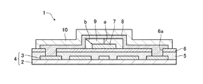
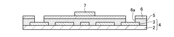
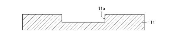
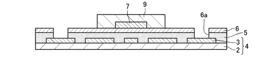
【解決手段】プリント配線基板1は、ベース基板4上に第1のジャンパ回路7を形成し、凹部が形成されたPETフィルム11に複数層のジャンパ回路7,8間の絶縁層9を構成するレジスト12を印刷し、PETフィルム11をベース基板4に対し、第1のジャンパ回路7と凹部11aとが対向するように位置合わせを行った上で貼り合わせ、レジスト12をベース基板4に転写し、レジスト12により絶縁層9をパターン形成し、絶縁層9が形成されたベース基板4上に第2のジャンパ回路8を形成して製造される。
【選択図】図1
Description
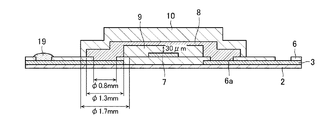
2 ベース基材
3 配線回路
4 ベース基板
5 接着剤
6 カバーレイ
6a 貫通孔
7 第1ジャンパ回路
8 第2ジャンパ回路
9 第1絶縁層
10 第2絶縁層
Claims (8)
- 配線パターンが形成されたベース基板上にジャンパ線を複数層有するプリント配線基板の製造方法において、
前記ベース基板上に第1のジャンパ線を形成する工程と、
凹部が形成された転写体に前記複数層のジャンパ線間の絶縁層を構成するレジストインクを印刷する工程と、
前記転写体を前記ベース基板に対し、前記第1のジャンパ線と前記凹部とが対向するように位置合わせを行った上で貼り合わせ、前記レジストインクを前記ベース基板に転写し、前記絶縁層を形成する工程と、
前記絶縁層が形成されたベース基板上に第2のジャンパ線を形成する工程とを備えた
ことを特徴とするプリント配線基板の製造方法。 - 前記レジストインクは感光性レジストインクであり、前記絶縁層はフォトリソグラフィによってパターン形成される
ことを特徴とする請求項1記載のプリント配線基板の製造方法。 - 前記絶縁層は、前記転写体を前記ベース基板に貼り合わせた状態のままマスクを介して前記レジストインクを露光することによりパターン形成される
ことを特徴とする請求項2記載のプリント配線基板の製造方法。 - 前記絶縁層は、前記レジストインクの露光後に前記転写体を剥離して現像することによりパターン形成される
ことを特徴とする請求項3記載のプリント配線基板の製造方法。 - 前記レジストインクは熱硬化性レジストインクである
ことを特徴とする請求項1記載のプリント配線基板の製造方法。 - 配線パターンが形成されたベース基板上にジャンパ線を複数層有するプリント配線基板において、
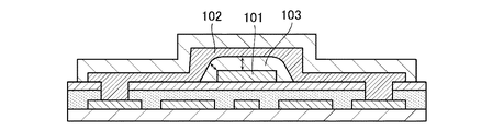
前記複数層のジャンパ線間の絶縁層は矩形状断面を有するように形成されている
ことを特徴とするプリント配線基板。 - 配線パターンが形成されたベース基板上にジャンパ線を複数層有するプリント配線基板の製造方法において、
前記ベース基板上に第1のジャンパ線を形成する工程と、
凹部が形成された転写体に前記複数層のジャンパ線間の絶縁層を構成するレジストインクを印刷する工程と、
前記転写体を前記ベース基板に対し、前記第1のジャンパ線と前記凹部とが対向するように位置合わせを行った上で貼り合わせ、前記レジストインクを前記ベース基板に転写し、前記絶縁層を形成する工程と、
前記レジストインクにより前記絶縁層を階段状断面を有するようにパターン形成する工程と、
前記絶縁層が形成されたベース基板上に第2のジャンパ線を形成する工程とを備えた
ことを特徴とするプリント配線基板の製造方法。 - 配線パターンが形成されたベース基板上にジャンパ線を複数層有するプリント配線基板において、
前記複数層のジャンパ線間の絶縁層は階段状断面を有するように形成されている
ことを特徴とするプリント配線基板。
Priority Applications (1)
| Application Number | Priority Date | Filing Date | Title |
|---|---|---|---|
| JP2011124005A JP5413748B2 (ja) | 2011-06-02 | 2011-06-02 | プリント配線基板及びその製造方法 |
Applications Claiming Priority (1)
| Application Number | Priority Date | Filing Date | Title |
|---|---|---|---|
| JP2011124005A JP5413748B2 (ja) | 2011-06-02 | 2011-06-02 | プリント配線基板及びその製造方法 |
Publications (2)
| Publication Number | Publication Date |
|---|---|
| JP2012253169A true JP2012253169A (ja) | 2012-12-20 |
| JP5413748B2 JP5413748B2 (ja) | 2014-02-12 |
Family
ID=47525721
Family Applications (1)
| Application Number | Title | Priority Date | Filing Date |
|---|---|---|---|
| JP2011124005A Expired - Fee Related JP5413748B2 (ja) | 2011-06-02 | 2011-06-02 | プリント配線基板及びその製造方法 |
Country Status (1)
| Country | Link |
|---|---|
| JP (1) | JP5413748B2 (ja) |
Cited By (1)
| Publication number | Priority date | Publication date | Assignee | Title |
|---|---|---|---|---|
| CN112616241A (zh) * | 2020-12-08 | 2021-04-06 | 捷讯精密橡胶(苏州)有限公司 | 一种印刷保护膜的柔性线路板及其生产工艺 |
Citations (5)
| Publication number | Priority date | Publication date | Assignee | Title |
|---|---|---|---|---|
| JPS63185276U (ja) * | 1987-05-19 | 1988-11-29 | ||
| JPH08186375A (ja) * | 1994-12-29 | 1996-07-16 | Dainippon Printing Co Ltd | 多層プリント配線板およびその製造方法 |
| JPH11233945A (ja) * | 1998-02-17 | 1999-08-27 | Dainippon Printing Co Ltd | 多層配線基板とその製造方法 |
| JP2006319254A (ja) * | 2005-05-16 | 2006-11-24 | Matsushita Electric Ind Co Ltd | 多層配線基板の製造方法 |
| JP2007059184A (ja) * | 2005-08-24 | 2007-03-08 | Citizen Electronics Co Ltd | キーシートモジュール |
-
2011
- 2011-06-02 JP JP2011124005A patent/JP5413748B2/ja not_active Expired - Fee Related
Patent Citations (5)
| Publication number | Priority date | Publication date | Assignee | Title |
|---|---|---|---|---|
| JPS63185276U (ja) * | 1987-05-19 | 1988-11-29 | ||
| JPH08186375A (ja) * | 1994-12-29 | 1996-07-16 | Dainippon Printing Co Ltd | 多層プリント配線板およびその製造方法 |
| JPH11233945A (ja) * | 1998-02-17 | 1999-08-27 | Dainippon Printing Co Ltd | 多層配線基板とその製造方法 |
| JP2006319254A (ja) * | 2005-05-16 | 2006-11-24 | Matsushita Electric Ind Co Ltd | 多層配線基板の製造方法 |
| JP2007059184A (ja) * | 2005-08-24 | 2007-03-08 | Citizen Electronics Co Ltd | キーシートモジュール |
Cited By (1)
| Publication number | Priority date | Publication date | Assignee | Title |
|---|---|---|---|---|
| CN112616241A (zh) * | 2020-12-08 | 2021-04-06 | 捷讯精密橡胶(苏州)有限公司 | 一种印刷保护膜的柔性线路板及其生产工艺 |
Also Published As
| Publication number | Publication date |
|---|---|
| JP5413748B2 (ja) | 2014-02-12 |
Similar Documents
| Publication | Publication Date | Title |
|---|---|---|
| US7346982B2 (en) | Method of fabricating printed circuit board having thin core layer | |
| US9955580B2 (en) | Method of manufacturing rigid-flexible printed circuit board | |
| JP5010737B2 (ja) | プリント配線板 | |
| KR100796983B1 (ko) | 인쇄회로기판 및 그 제조방법 | |
| JP5997260B2 (ja) | 印刷回路基板及びその製造方法 | |
| JP5097827B2 (ja) | フレックスリジッド配線板及び電子デバイス | |
| US20130003314A1 (en) | Multilayer printed circuit board and manufacturing method therefor | |
| TWI479972B (zh) | Multi - layer flexible printed wiring board and manufacturing method thereof | |
| JPWO2008155957A1 (ja) | 部品内蔵基板の製造方法および部品内蔵基板 | |
| WO2010007704A1 (ja) | フレックスリジッド配線板及び電子デバイス | |
| CN109788666B (zh) | 线路基板及其制作方法 | |
| TW201334647A (zh) | 多層配線基板及其製造方法 | |
| US20070272654A1 (en) | Method for Manufacturing Circuit Board | |
| CN1751547B (zh) | 多层基板及其制造方法 | |
| JP4183708B2 (ja) | 部品内蔵基板の製造方法 | |
| CN106455312A (zh) | 布线基板以及其制造方法 | |
| JP5302920B2 (ja) | 多層配線基板の製造方法 | |
| KR102857786B1 (ko) | 회로 기판, 회로 기판의 제조 방법 및 전자 기기 | |
| US20190327830A1 (en) | Printed wiring board and method for manufacturing the same | |
| CN109788664B (zh) | 一种线路基板及其制作方法 | |
| JP6099902B2 (ja) | 配線基板の製造方法 | |
| CN114449781B (zh) | 内埋元件电路板的制造方法 | |
| JP5413748B2 (ja) | プリント配線基板及びその製造方法 | |
| JP4497548B2 (ja) | 配線基板 | |
| JP2005175185A (ja) | フレキシブル配線基板 |
Legal Events
| Date | Code | Title | Description |
|---|---|---|---|
| A977 | Report on retrieval |
Free format text: JAPANESE INTERMEDIATE CODE: A971007 Effective date: 20130328 |
|
| A131 | Notification of reasons for refusal |
Free format text: JAPANESE INTERMEDIATE CODE: A131 Effective date: 20130402 |
|
| A521 | Request for written amendment filed |
Free format text: JAPANESE INTERMEDIATE CODE: A523 Effective date: 20130513 |
|
| TRDD | Decision of grant or rejection written | ||
| A01 | Written decision to grant a patent or to grant a registration (utility model) |
Free format text: JAPANESE INTERMEDIATE CODE: A01 Effective date: 20131015 |
|
| A61 | First payment of annual fees (during grant procedure) |
Free format text: JAPANESE INTERMEDIATE CODE: A61 Effective date: 20131031 |
|
| R150 | Certificate of patent or registration of utility model |
Ref document number: 5413748 Country of ref document: JP Free format text: JAPANESE INTERMEDIATE CODE: R150 |
|
| R250 | Receipt of annual fees |
Free format text: JAPANESE INTERMEDIATE CODE: R250 |
|
| R250 | Receipt of annual fees |
Free format text: JAPANESE INTERMEDIATE CODE: R250 |
|
| R250 | Receipt of annual fees |
Free format text: JAPANESE INTERMEDIATE CODE: R250 |
|
| R250 | Receipt of annual fees |
Free format text: JAPANESE INTERMEDIATE CODE: R250 |
|
| R250 | Receipt of annual fees |
Free format text: JAPANESE INTERMEDIATE CODE: R250 |
|
| R250 | Receipt of annual fees |
Free format text: JAPANESE INTERMEDIATE CODE: R250 |
|
| R250 | Receipt of annual fees |
Free format text: JAPANESE INTERMEDIATE CODE: R250 |
|
| LAPS | Cancellation because of no payment of annual fees |