JP2012253178A - Thermoelectric conversion element, method for manufacturing the same, and thermoelectric conversion module - Google Patents
Thermoelectric conversion element, method for manufacturing the same, and thermoelectric conversion module Download PDFInfo
- Publication number
- JP2012253178A JP2012253178A JP2011124262A JP2011124262A JP2012253178A JP 2012253178 A JP2012253178 A JP 2012253178A JP 2011124262 A JP2011124262 A JP 2011124262A JP 2011124262 A JP2011124262 A JP 2011124262A JP 2012253178 A JP2012253178 A JP 2012253178A
- Authority
- JP
- Japan
- Prior art keywords
- nanowire
- thermoelectric conversion
- electrode
- conversion element
- semiconductor material
- Prior art date
- Legal status (The legal status is an assumption and is not a legal conclusion. Google has not performed a legal analysis and makes no representation as to the accuracy of the status listed.)
- Withdrawn
Links
- 238000006243 chemical reaction Methods 0.000 title claims abstract description 132
- 238000004519 manufacturing process Methods 0.000 title claims abstract description 26
- 238000000034 method Methods 0.000 title abstract description 25
- 239000002070 nanowire Substances 0.000 claims abstract description 217
- 239000004065 semiconductor Substances 0.000 claims abstract description 121
- 239000000463 material Substances 0.000 claims abstract description 113
- 239000002019 doping agent Substances 0.000 claims abstract description 55
- 230000005291 magnetic effect Effects 0.000 claims description 33
- 239000000696 magnetic material Substances 0.000 claims description 19
- 239000003054 catalyst Substances 0.000 claims description 12
- 239000002243 precursor Substances 0.000 claims description 12
- 239000003795 chemical substances by application Substances 0.000 claims description 8
- 230000001590 oxidative effect Effects 0.000 claims description 3
- 239000000758 substrate Substances 0.000 description 33
- 229910052751 metal Inorganic materials 0.000 description 15
- 239000002184 metal Substances 0.000 description 15
- 239000003638 chemical reducing agent Substances 0.000 description 10
- XEEYBQQBJWHFJM-UHFFFAOYSA-N Iron Chemical compound [Fe] XEEYBQQBJWHFJM-UHFFFAOYSA-N 0.000 description 9
- 238000010586 diagram Methods 0.000 description 9
- 238000002955 isolation Methods 0.000 description 9
- OKTJSMMVPCPJKN-UHFFFAOYSA-N Carbon Chemical compound [C] OKTJSMMVPCPJKN-UHFFFAOYSA-N 0.000 description 8
- 239000000969 carrier Substances 0.000 description 8
- 239000010419 fine particle Substances 0.000 description 7
- 239000002041 carbon nanotube Substances 0.000 description 6
- 229910021393 carbon nanotube Inorganic materials 0.000 description 6
- 230000003993 interaction Effects 0.000 description 6
- BASFCYQUMIYNBI-UHFFFAOYSA-N platinum Chemical compound [Pt] BASFCYQUMIYNBI-UHFFFAOYSA-N 0.000 description 6
- 239000000126 substance Substances 0.000 description 6
- 230000007423 decrease Effects 0.000 description 5
- 230000007547 defect Effects 0.000 description 5
- 238000009792 diffusion process Methods 0.000 description 5
- 238000010248 power generation Methods 0.000 description 5
- 230000008569 process Effects 0.000 description 5
- PXHVJJICTQNCMI-UHFFFAOYSA-N Nickel Chemical compound [Ni] PXHVJJICTQNCMI-UHFFFAOYSA-N 0.000 description 4
- 230000005678 Seebeck effect Effects 0.000 description 4
- 239000000443 aerosol Substances 0.000 description 4
- 238000000151 deposition Methods 0.000 description 4
- 239000007769 metal material Substances 0.000 description 4
- 229910000859 α-Fe Inorganic materials 0.000 description 4
- 230000005355 Hall effect Effects 0.000 description 3
- 230000005535 acoustic phonon Effects 0.000 description 3
- 239000011575 calcium Substances 0.000 description 3
- 239000003575 carbonaceous material Substances 0.000 description 3
- 238000005229 chemical vapour deposition Methods 0.000 description 3
- 239000006185 dispersion Substances 0.000 description 3
- 230000000694 effects Effects 0.000 description 3
- 238000002003 electron diffraction Methods 0.000 description 3
- 239000010931 gold Substances 0.000 description 3
- 229910001385 heavy metal Inorganic materials 0.000 description 3
- 229910052742 iron Inorganic materials 0.000 description 3
- 238000005304 joining Methods 0.000 description 3
- VNWKTOKETHGBQD-UHFFFAOYSA-N methane Chemical compound C VNWKTOKETHGBQD-UHFFFAOYSA-N 0.000 description 3
- 230000000737 periodic effect Effects 0.000 description 3
- 238000004544 sputter deposition Methods 0.000 description 3
- XMWRBQBLMFGWIX-UHFFFAOYSA-N C60 fullerene Chemical compound C12=C3C(C4=C56)=C7C8=C5C5=C9C%10=C6C6=C4C1=C1C4=C6C6=C%10C%10=C9C9=C%11C5=C8C5=C8C7=C3C3=C7C2=C1C1=C2C4=C6C4=C%10C6=C9C9=C%11C5=C5C8=C3C3=C7C1=C1C2=C4C6=C2C9=C5C3=C12 XMWRBQBLMFGWIX-UHFFFAOYSA-N 0.000 description 2
- OYPRJOBELJOOCE-UHFFFAOYSA-N Calcium Chemical compound [Ca] OYPRJOBELJOOCE-UHFFFAOYSA-N 0.000 description 2
- ZLMJMSJWJFRBEC-UHFFFAOYSA-N Potassium Chemical compound [K] ZLMJMSJWJFRBEC-UHFFFAOYSA-N 0.000 description 2
- 229910000577 Silicon-germanium Inorganic materials 0.000 description 2
- 238000010521 absorption reaction Methods 0.000 description 2
- 229910052782 aluminium Inorganic materials 0.000 description 2
- XAGFODPZIPBFFR-UHFFFAOYSA-N aluminium Chemical compound [Al] XAGFODPZIPBFFR-UHFFFAOYSA-N 0.000 description 2
- 230000004888 barrier function Effects 0.000 description 2
- 229910052791 calcium Inorganic materials 0.000 description 2
- 230000008859 change Effects 0.000 description 2
- 229910052802 copper Inorganic materials 0.000 description 2
- 239000010949 copper Substances 0.000 description 2
- 230000008021 deposition Effects 0.000 description 2
- 239000002079 double walled nanotube Substances 0.000 description 2
- 230000005684 electric field Effects 0.000 description 2
- 230000005611 electricity Effects 0.000 description 2
- 230000005294 ferromagnetic effect Effects 0.000 description 2
- 239000003302 ferromagnetic material Substances 0.000 description 2
- 239000000835 fiber Substances 0.000 description 2
- 229910003472 fullerene Inorganic materials 0.000 description 2
- 239000002223 garnet Substances 0.000 description 2
- 239000007789 gas Substances 0.000 description 2
- 239000011521 glass Substances 0.000 description 2
- 229910052737 gold Inorganic materials 0.000 description 2
- -1 hydrocarbon organic compound Chemical class 0.000 description 2
- 238000003384 imaging method Methods 0.000 description 2
- 239000012535 impurity Substances 0.000 description 2
- 238000002347 injection Methods 0.000 description 2
- 239000007924 injection Substances 0.000 description 2
- 239000012212 insulator Substances 0.000 description 2
- 230000031700 light absorption Effects 0.000 description 2
- 238000005259 measurement Methods 0.000 description 2
- 239000002048 multi walled nanotube Substances 0.000 description 2
- 229910052759 nickel Inorganic materials 0.000 description 2
- 230000003647 oxidation Effects 0.000 description 2
- 238000007254 oxidation reaction Methods 0.000 description 2
- SLIUAWYAILUBJU-UHFFFAOYSA-N pentacene Chemical compound C1=CC=CC2=CC3=CC4=CC5=CC=CC=C5C=C4C=C3C=C21 SLIUAWYAILUBJU-UHFFFAOYSA-N 0.000 description 2
- 229910052697 platinum Inorganic materials 0.000 description 2
- 229910052700 potassium Inorganic materials 0.000 description 2
- 239000011591 potassium Substances 0.000 description 2
- 239000002109 single walled nanotube Substances 0.000 description 2
- 229910052596 spinel Inorganic materials 0.000 description 2
- 239000011029 spinel Substances 0.000 description 2
- PCCVSPMFGIFTHU-UHFFFAOYSA-N tetracyanoquinodimethane Chemical compound N#CC(C#N)=C1C=CC(=C(C#N)C#N)C=C1 PCCVSPMFGIFTHU-UHFFFAOYSA-N 0.000 description 2
- FHCPAXDKURNIOZ-UHFFFAOYSA-N tetrathiafulvalene Chemical compound S1C=CSC1=C1SC=CS1 FHCPAXDKURNIOZ-UHFFFAOYSA-N 0.000 description 2
- 238000012546 transfer Methods 0.000 description 2
- JBRZTFJDHDCESZ-UHFFFAOYSA-N AsGa Chemical compound [As]#[Ga] JBRZTFJDHDCESZ-UHFFFAOYSA-N 0.000 description 1
- NLZUEZXRPGMBCV-UHFFFAOYSA-N Butylhydroxytoluene Chemical compound CC1=CC(C(C)(C)C)=C(O)C(C(C)(C)C)=C1 NLZUEZXRPGMBCV-UHFFFAOYSA-N 0.000 description 1
- 239000004215 Carbon black (E152) Substances 0.000 description 1
- RYGMFSIKBFXOCR-UHFFFAOYSA-N Copper Chemical compound [Cu] RYGMFSIKBFXOCR-UHFFFAOYSA-N 0.000 description 1
- 101100167360 Drosophila melanogaster chb gene Proteins 0.000 description 1
- WHXSMMKQMYFTQS-UHFFFAOYSA-N Lithium Chemical compound [Li] WHXSMMKQMYFTQS-UHFFFAOYSA-N 0.000 description 1
- 229910002665 PbTe Inorganic materials 0.000 description 1
- 229910004298 SiO 2 Inorganic materials 0.000 description 1
- VYPSYNLAJGMNEJ-UHFFFAOYSA-N Silicium dioxide Chemical compound O=[Si]=O VYPSYNLAJGMNEJ-UHFFFAOYSA-N 0.000 description 1
- XUIMIQQOPSSXEZ-UHFFFAOYSA-N Silicon Chemical compound [Si] XUIMIQQOPSSXEZ-UHFFFAOYSA-N 0.000 description 1
- LEVVHYCKPQWKOP-UHFFFAOYSA-N [Si].[Ge] Chemical compound [Si].[Ge] LEVVHYCKPQWKOP-UHFFFAOYSA-N 0.000 description 1
- 239000000956 alloy Substances 0.000 description 1
- 239000012298 atmosphere Substances 0.000 description 1
- QVGXLLKOCUKJST-UHFFFAOYSA-N atomic oxygen Chemical compound [O] QVGXLLKOCUKJST-UHFFFAOYSA-N 0.000 description 1
- 230000008901 benefit Effects 0.000 description 1
- 229910052797 bismuth Inorganic materials 0.000 description 1
- 238000004364 calculation method Methods 0.000 description 1
- 229910052799 carbon Inorganic materials 0.000 description 1
- 230000015556 catabolic process Effects 0.000 description 1
- 239000011248 coating agent Substances 0.000 description 1
- 238000000576 coating method Methods 0.000 description 1
- 229910000428 cobalt oxide Inorganic materials 0.000 description 1
- IVMYJDGYRUAWML-UHFFFAOYSA-N cobalt(ii) oxide Chemical compound [Co]=O IVMYJDGYRUAWML-UHFFFAOYSA-N 0.000 description 1
- 150000001875 compounds Chemical class 0.000 description 1
- 239000004020 conductor Substances 0.000 description 1
- 239000000470 constituent Substances 0.000 description 1
- 238000010276 construction Methods 0.000 description 1
- 238000001816 cooling Methods 0.000 description 1
- 239000013078 crystal Substances 0.000 description 1
- 238000006731 degradation reaction Methods 0.000 description 1
- 238000011161 development Methods 0.000 description 1
- 230000018109 developmental process Effects 0.000 description 1
- 239000010432 diamond Substances 0.000 description 1
- 229910003460 diamond Inorganic materials 0.000 description 1
- 230000008034 disappearance Effects 0.000 description 1
- 238000010292 electrical insulation Methods 0.000 description 1
- 238000002848 electrochemical method Methods 0.000 description 1
- 238000011156 evaluation Methods 0.000 description 1
- 230000005293 ferrimagnetic effect Effects 0.000 description 1
- 239000002902 ferrimagnetic material Substances 0.000 description 1
- ZPDRQAVGXHVGTB-UHFFFAOYSA-N gallium;gadolinium(3+);oxygen(2-) Chemical compound [O-2].[O-2].[O-2].[Ga+3].[Gd+3] ZPDRQAVGXHVGTB-UHFFFAOYSA-N 0.000 description 1
- PCHJSUWPFVWCPO-UHFFFAOYSA-N gold Chemical compound [Au] PCHJSUWPFVWCPO-UHFFFAOYSA-N 0.000 description 1
- 229910021389 graphene Inorganic materials 0.000 description 1
- 238000010438 heat treatment Methods 0.000 description 1
- 239000011019 hematite Substances 0.000 description 1
- 229910052595 hematite Inorganic materials 0.000 description 1
- 229930195733 hydrocarbon Natural products 0.000 description 1
- RPQDHPTXJYYUPQ-UHFFFAOYSA-N indium arsenide Chemical compound [In]#[As] RPQDHPTXJYYUPQ-UHFFFAOYSA-N 0.000 description 1
- 239000011810 insulating material Substances 0.000 description 1
- MTRJKZUDDJZTLA-UHFFFAOYSA-N iron yttrium Chemical compound [Fe].[Y] MTRJKZUDDJZTLA-UHFFFAOYSA-N 0.000 description 1
- LIKBJVNGSGBSGK-UHFFFAOYSA-N iron(3+);oxygen(2-) Chemical compound [O-2].[O-2].[O-2].[Fe+3].[Fe+3] LIKBJVNGSGBSGK-UHFFFAOYSA-N 0.000 description 1
- 229910052745 lead Inorganic materials 0.000 description 1
- 229910001338 liquidmetal Inorganic materials 0.000 description 1
- 229910052744 lithium Inorganic materials 0.000 description 1
- 230000005389 magnetism Effects 0.000 description 1
- 230000005415 magnetization Effects 0.000 description 1
- 238000002844 melting Methods 0.000 description 1
- 230000008018 melting Effects 0.000 description 1
- 238000001465 metallisation Methods 0.000 description 1
- 239000000203 mixture Substances 0.000 description 1
- 238000012986 modification Methods 0.000 description 1
- 230000004048 modification Effects 0.000 description 1
- 230000003287 optical effect Effects 0.000 description 1
- 229910052760 oxygen Inorganic materials 0.000 description 1
- 239000001301 oxygen Substances 0.000 description 1
- KDLHZDBZIXYQEI-UHFFFAOYSA-N palladium Substances [Pd] KDLHZDBZIXYQEI-UHFFFAOYSA-N 0.000 description 1
- 238000005498 polishing Methods 0.000 description 1
- 238000007639 printing Methods 0.000 description 1
- 239000002994 raw material Substances 0.000 description 1
- 230000009467 reduction Effects 0.000 description 1
- 229910052701 rubidium Inorganic materials 0.000 description 1
- IGLNJRXAVVLDKE-UHFFFAOYSA-N rubidium atom Chemical compound [Rb] IGLNJRXAVVLDKE-UHFFFAOYSA-N 0.000 description 1
- 238000007650 screen-printing Methods 0.000 description 1
- 230000035945 sensitivity Effects 0.000 description 1
- 239000010703 silicon Substances 0.000 description 1
- 229910052710 silicon Inorganic materials 0.000 description 1
- 229910052814 silicon oxide Inorganic materials 0.000 description 1
- 239000002210 silicon-based material Substances 0.000 description 1
- 238000003980 solgel method Methods 0.000 description 1
- 239000007787 solid Substances 0.000 description 1
- 230000005418 spin wave Effects 0.000 description 1
- 238000005507 spraying Methods 0.000 description 1
- 238000006467 substitution reaction Methods 0.000 description 1
- OCGWQDWYSQAFTO-UHFFFAOYSA-N tellanylidenelead Chemical compound [Pb]=[Te] OCGWQDWYSQAFTO-UHFFFAOYSA-N 0.000 description 1
- 229910052714 tellurium Inorganic materials 0.000 description 1
- 238000007740 vapor deposition Methods 0.000 description 1
- 239000002918 waste heat Substances 0.000 description 1
- 229910052727 yttrium Inorganic materials 0.000 description 1
- VWQVUPCCIRVNHF-UHFFFAOYSA-N yttrium atom Chemical compound [Y] VWQVUPCCIRVNHF-UHFFFAOYSA-N 0.000 description 1
Images



Landscapes
- Hall/Mr Elements (AREA)
Abstract
Description
本発明は、熱を電気に変換する熱電変換素子及びその製造方法に関する。また、本発明は、当該熱電変換素子を有する熱電変換モジュールに関する。 The present invention relates to a thermoelectric conversion element that converts heat into electricity and a method for manufacturing the same. Moreover, this invention relates to the thermoelectric conversion module which has the said thermoelectric conversion element.
近年、Bi、Te、Pbなどの重金属を熱電変換素子に用いて、巨大施設での発生熱を、電力に還元する発電装置が開発されている。熱電変換とは熱エネルギーを電気エネルギーに変換することである。この熱電変換は、2種類の物質を接合させて両端に温度差を生じさせると、温度勾配に逆行するように電圧が発生するというゼーベック効果が基本になっている。例えば、Bi2Te3等、キャリアの移動度が常温で高いバルク半導体材料にドーピングし、電子が移動するn型半導体と正孔が移動するp型半導体の2種類の半導体物質を、高温部と低温部の2つの金属電極に挟んだ熱電変換素子が作製されている。これにより、電子・正孔のキャリアが高温部から低温部に流れ、起電力が発生し発電する。実用化されている熱電変換装置においては、この基本素子を複数個配置してモジュール化することにより発電効率を高めている。 In recent years, power generators have been developed that use heavy metals such as Bi, Te, and Pb as thermoelectric conversion elements to reduce the heat generated in huge facilities to electric power. Thermoelectric conversion is the conversion of thermal energy into electrical energy. This thermoelectric conversion is based on the Seebeck effect in which, when two kinds of materials are joined together and a temperature difference is generated at both ends, a voltage is generated so as to go against the temperature gradient. For example, a bulk semiconductor material having a high carrier mobility at room temperature, such as Bi 2 Te 3 , is doped with two types of semiconductor substances, an n-type semiconductor in which electrons move and a p-type semiconductor in which holes move, A thermoelectric conversion element sandwiched between two metal electrodes in the low temperature part is produced. As a result, electron / hole carriers flow from the high temperature portion to the low temperature portion, and an electromotive force is generated to generate power. In a thermoelectric conversion device in practical use, the power generation efficiency is increased by arranging a plurality of these basic elements into a module.
この他にも、発電効率を高める構造や材料が提案されている(例えば、非特許文献1〜3参照)。非特許文献1においては、コバルト酸化物を用いた熱電変換の効率を測定している。非特許文献2においては、スピン流を利用したスピンゼーベック効果による、磁性体を用いたスピン熱電変換について示されている。また、非特許文献3においては、通常のシリコン材料を次元の低いナノワイヤ構造にすることによって熱電変換効率が大きく増大することが示されている。
In addition, structures and materials that improve power generation efficiency have been proposed (see, for example, Non-Patent
また、熱電変換素子の信頼性を高める手段も開示されている(例えば、特許文献1及び2参照)。特許文献1においては、基板と、当該基板と接触する側の電極の少なくとも一方が、電気的な絶縁性を有し、当該基板と当該電極が液体金属により接合する構造を有し、電極と熱電半導体の接合部が、金属繊維を含有する熱電変換素子が開示されている。特許文献2においては、対向する一対の電極に挟まれたp、n熱電半導体対からなり、該電極と該熱電半導体間に金属を内包したカーボンナノチューブからなる応力緩和層を有する熱電変換素子が開示されている。
In addition, means for improving the reliability of the thermoelectric conversion element is also disclosed (for example, see
以下の分析は、本発明の観点から与えられる。 The following analysis is given from the perspective of the present invention.
現在常温で使用されているバルクな高移動度半導体を用いた熱電変換素子にはいくつかの問題がある。第1の問題点は、これらのバルクな半導体材料は、その構造のために、耐酸化性が低く、劣化しやすいということである。このため、半導体材料に加工を施すことが容易ではなく、この半導体材料では熱電変換のさらなる高効率化を図ることができない。第2の問題点は、金属電極とのコンタクト接合部における原子レベルでの制御が困難であるので、金属電極とバルクの半導体材料のコンタクト接合部において金属原子と半導体原子が原子拡散により混ざってしまうということである。このため、熱電効率は大幅に低下してしまうことになる。 There are several problems with thermoelectric conversion elements using bulk high mobility semiconductors currently used at room temperature. The first problem is that these bulk semiconductor materials have low oxidation resistance and are susceptible to degradation due to their structure. For this reason, it is not easy to process the semiconductor material, and with this semiconductor material, it is not possible to further increase the efficiency of thermoelectric conversion. The second problem is that it is difficult to control at the atomic level in the contact junction with the metal electrode, so that metal atoms and semiconductor atoms are mixed by atomic diffusion in the contact junction between the metal electrode and the bulk semiconductor material. That's what it means. For this reason, thermoelectric efficiency will fall significantly.
特許文献1に記載の熱電変換素子においては、電極と熱電半導体との間には、密着性を高めると共に、高い熱伝導性を確保するために金属繊維が設けられている。しかしながら、熱伝導性を高めると、熱電効率を向上させることはできない。特許文献2に記載の熱電変換素子においても、カーボンナノチューブに金属を内包させると熱伝導率が高くなることになる。したがって、特許文献2に記載の応力緩和層を用いると、熱電効率を向上させることはできない。
In the thermoelectric conversion element described in
一般に、熱電変換素子において、熱エネルギーから電気エネルギーへの変換効率ηは、以下の式1のように表すことができる。ここでTHは高温部の温度、TCは低温部の温度、Tは平均温度T=(TH+TC)/2である。Zは熱電性能指数と呼ばれ、物質とその構造によって決定される材料特有の物理量であり、以下の式2で表される。Gは電子・正孔のキャリア伝導率である。κは熱伝導率である。Sはゼーベック係数である。ゼーベック係数Sは、物質材料に固有の物理量であり、流れる電子・正孔のキャリアの移動度とそのフェルミ面での状態密度によって決まる。
In general, in a thermoelectric conversion element, the conversion efficiency η from heat energy to electric energy can be expressed as the following
[式1]
[式2]
式1に示す変換効率ηは、変数ZTに対して単調に増加する関数であり、大きいZTを得ることが高効率な熱電変換素子の構築につながる。温度勾配による発電にて得られる起電力ΔVはゼーベック係数Sと温度差ΔTを用いて式3のように表される。したがって、大きい熱電効率を達成するためには、キャリアの伝導度を高め、一方熱伝導を低くすることが必要となる。また、高いキャリア伝導が得られるとそれに伴って得られる起電力も大きくなる。
The conversion efficiency η shown in
[式3]
一般にこの無次元量のZTが1を超えれば優良な熱電交換性能を持つとされている。通常の物質では、電子の移動度が高ければ熱の伝導度も高くなり、性能評価指数ZTは大きくならず熱電変換機能は小さくなる。現在実用化されている重金属のレアメタルを含んだ高移動度のバルク半導体材料は、フェルミ面に高い状態密度を持つ層状化合物のため、キャリアの移動度が大きく熱移動度が小さい。また、このバルク半導体材料は、層状内へのドーピングが容易でもある。しかし、このバルク半導体の熱伝効率を更に高めることは非常に困難であり、またレアメタルを用いるため資源量の観点からも別の材料を併用、または代用した高効率な熱電変換素子が求められている。 In general, if this dimensionless amount of ZT exceeds 1, it is said that the thermoelectric exchange performance is excellent. In a normal substance, the higher the electron mobility, the higher the thermal conductivity, and the performance evaluation index ZT does not increase and the thermoelectric conversion function decreases. A high mobility bulk semiconductor material containing a rare metal, which is currently in practical use, is a layered compound having a high state density on the Fermi surface, and therefore has a high carrier mobility and a low thermal mobility. This bulk semiconductor material is also easy to dope into layers. However, it is very difficult to further increase the heat transfer efficiency of this bulk semiconductor, and since a rare metal is used, there is a need for a highly efficient thermoelectric conversion element that uses another material or substitutes it from the viewpoint of the amount of resources. Yes.
本発明の第1視点によれば、熱電変換材料である半導体材料と、半導体材料に電気的に接続された少なくとも1つのナノワイヤと、ナノワイヤと電気的に接続された電極と、を備える熱電変換素子が提供される。ナノワイヤは、半導体基材と、半導体基材の表面に付着したドーパントと、を有する。 According to a first aspect of the present invention, a thermoelectric conversion element comprising: a semiconductor material that is a thermoelectric conversion material; at least one nanowire that is electrically connected to the semiconductor material; and an electrode that is electrically connected to the nanowire. Is provided. The nanowire has a semiconductor substrate and a dopant attached to the surface of the semiconductor substrate.
本発明の第2視点によれば、絶縁性を有する磁性体と、磁性体と磁気的に接続された磁性材料を含有する少なくとも1つのナノワイヤと、ナノワイヤと磁気的に接続された電極と、を備える熱電変換素子が提供される。 According to a second aspect of the present invention, an insulating magnetic material, at least one nanowire containing a magnetic material magnetically connected to the magnetic material, and an electrode magnetically connected to the nanowire, A thermoelectric conversion element is provided.
本発明の第3視点によれば、上記第1視点又は第2視点に記載の熱電変換素子を複数配列した熱電変換モジュールが提供される。 According to a third aspect of the present invention, there is provided a thermoelectric conversion module in which a plurality of thermoelectric conversion elements described in the first viewpoint or the second viewpoint are arranged.
本発明の第4視点によれば、電極上に触媒を供給する工程と、電極の上方に半導体材料を配置する工程と、ナノワイヤの先端が半導体材料に接合又は接触するように、触媒からナノワイヤを成長させる工程と、ナノワイヤの表面にドーパントを付着させる工程と、を含む熱電変換素子の製造方法が提供される。 According to the fourth aspect of the present invention, the step of supplying the catalyst on the electrode, the step of disposing the semiconductor material above the electrode, and the nanowire from the catalyst so that the tip of the nanowire is joined or contacted with the semiconductor material. There is provided a method of manufacturing a thermoelectric conversion element including a growing step and a step of attaching a dopant to the surface of a nanowire.
本発明の第5視点によれば、磁性体を形成する工程と、磁性体上にナノワイヤ前駆層を形成する工程と、ナノワイヤ前駆層上に電極を形成する工程と、ナノワイヤ前駆層を酸化させて、少なくとも1つのナノワイヤを形成する工程と、を含む熱電変換素子の製造方法が提供される。 According to a fifth aspect of the present invention, a step of forming a magnetic body, a step of forming a nanowire precursor layer on the magnetic body, a step of forming an electrode on the nanowire precursor layer, and oxidizing the nanowire precursor layer Forming at least one nanowire, and a method for manufacturing a thermoelectric conversion element.
本発明は、以下の効果のうち少なくとも1つを有する。 The present invention has at least one of the following effects.
本発明の熱電変換素子においては、電極と半導体材料又は磁性体との接合にナノワイヤを使用している。これにより、熱伝導性を低下させて、熱電変換効率を高めることができる。 In the thermoelectric conversion element of the present invention, nanowires are used for bonding the electrode and the semiconductor material or magnetic material. Thereby, thermal conductivity can be reduced and thermoelectric conversion efficiency can be improved.
本発明の熱電変換素子においては、電極と半導体材料とをナノワイヤで接合することにより、金属と半導体との原子拡散を抑制すると共に、電極から半導体材料へのキャリアの伝導性を高めることができる。これにより、熱電変換効率を高めることができる。 In the thermoelectric conversion element of the present invention, by joining the electrode and the semiconductor material with a nanowire, atomic diffusion between the metal and the semiconductor can be suppressed, and the conductivity of carriers from the electrode to the semiconductor material can be increased. Thereby, thermoelectric conversion efficiency can be improved.
本発明の熱電変換素子においては、電極と磁性体とをナノワイヤで接合することにより、電極から磁性体へのスピンの伝導性を高めることができる。これにより、熱電変換効率を高めることができる。 In the thermoelectric conversion element of the present invention, the conductivity of the spin from the electrode to the magnetic body can be increased by joining the electrode and the magnetic body with a nanowire. Thereby, thermoelectric conversion efficiency can be improved.
本発明の熱電変換素子の製造方法によれば、上記熱電変換素子を容易に製造することができる。 According to the method for manufacturing a thermoelectric conversion element of the present invention, the thermoelectric conversion element can be easily manufactured.
以下に、図面を参照して本発明の実施形態について説明する。 Embodiments of the present invention will be described below with reference to the drawings.
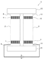
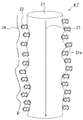
本発明の第1実施形態に係る熱電変換素子について説明する。図1に、本発明の第1実施形態に係る熱電変換素子の概略平面図を示す。図2にナノワイヤの模式図を示す。 The thermoelectric conversion element according to the first embodiment of the present invention will be described. In FIG. 1, the schematic plan view of the thermoelectric conversion element which concerns on 1st Embodiment of this invention is shown. FIG. 2 shows a schematic diagram of the nanowire.
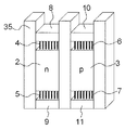
本発明の熱電変換素子1は、n型半導体材料2と、p型半導体材料3と、n型半導体材料2の両端に電気的に接続された第1電極8及び第2電極9と、p型半導体材料3の両端に電気的に接続された第3電極10及び第4電極11と、n型半導体材料2と第1電極8及び第2電極9との間に配され、これらを電気的に接続する少なくとも1つの第1ナノワイヤ4及び第2ナノワイヤ5と、p型半導体材料3と第3電極10及び第4電極11との間に配され、これらを電気的に接続する少なくとも1つの第3ナノワイヤ6及び第4ナノワイヤ7と、第1電極8及び第3電極10と熱的に接続された高温部12と、第2電極9及び第4電極11と熱的に接続された低温部13と、を備える。
The
n型半導体材料2及びp型半導体材料3としては、熱電変換材料として使用可能な半導体材料を使用することができ、例えば、BiTe系材料やPbTe系材料を使用することができる。
As the n-
第1〜第4ナノワイヤ4〜7は、線状構造(擬一次元構造)を有する半導体基材21と、その表面に付着したドーパント22を有する。ここで、「擬一次元」とは、電子の伝導方向において、長距離方向が確保されている次元数を意味する。すなわち、「擬一次元」とは、半導体材料2,3と電極8〜11とを結ぶ方向の長さ(1つのナノワイヤの長さ)が、その垂直方向の大きさ(1つのナノワイヤの直径に相当する大きさ)に対して非常に大きいことを意味する。例えば、第1〜第4ナノワイヤ4〜7の長さは、100ナノメートル〜1000ナノメートルであると好ましい。第1〜第4ナノワイヤ4〜7の太さは、1ナノメートル以上100ナノメートル以下であると好ましく、1ナノメートル以上10ナノメートル以下であるとより好ましい。直径が100ナノメートルを超えると本発明の効果が得られにくくなるので、100ナノメートル以下であると好ましい。
The 1st-4th nanowires 4-7 have the
第1〜第4ナノワイヤ4〜7は、ドーパント22により導電性を有するが、その熱伝導性は金属ナノワイヤに比べてはるかに小さい性質を有すると好ましい。
Although the 1st-4th nanowires 4-7 have electroconductivity by the
第1〜第4ナノワイヤ4〜7の半導体基材21は、重金属を含有していないと好ましい。ここでいう重金属とは、周期表5列目以下の元素(すなわちルビジウムRb以上の原子量を有する元素)である。第1〜第4ナノワイヤ4〜7の材料としては、シリコン(Si)系材料、シリコンゲルマニウム(SiGe)系材料、ガリウム砒素(GaAs)系材料、インジウム砒素(InAs)系材料、炭素(C)系材料等を使用することができる。炭素系材料の例としては、例えば、ダイヤモンド、グラフェン、カーボンナノチューブ類が挙げられる。炭素系材料は、高融点を有すると共に、ナノオーダーのサイズに形成しても化学的・機械的に安定であるので、デバイスとしての信頼性を高くすることができる。また、カーボンナノチューブ類は、ナノオーダーサイズに加工する必要がないという利点も有する。ここで、カーボンナノチューブ類とは、シングルウォールナノチューブ(SWNT)、ダブルウォールナノチューブ(DWNT)、マルチウォールナノチューブ(MWNT)、カーボンナノホーン等、筒状部分を有する炭素材料のことをいう。
It is preferable that the
第1〜第4ナノワイヤ4〜7は、半導体基材21の表面に、半導体としての機能を持たせるためのドーパント22を有する。n型半導体とする場合には、ナノワイヤに電荷供給型のドーパント22を付着させる。p型半導体とする場合には、ナノワイヤに電荷吸収型のドーパント22を付着させる。一般に成長したナノワイヤの表面は欠陥・乱れ21aを含む。そのため、フォノンの伝導は表面の欠陥・乱れ21aにより大きく低下する(非特許文献3参照)。更に、これに加えて周期的構造を乱すようにランダムにドーパント分子を吸着させることで電子・正孔のキャリア伝導を大きく下げることなく、フォノンによる熱伝導を大きく抑制することができる。なお、欠陥・乱れ21aとは、ナノワイヤ表面における原子欠陥や原子構造の乱れをいう。
The 1st-4th nanowires 4-7 have the
第1〜第4ナノワイヤ4〜7に半導体性能を付与するドーパント22としては、半導体基材21の構成元素の原子番号に近い元素を使用すると好ましい。ドーパント22としては、例えば炭化水素有機化合物を使用することができる。n型半導体である第1ナノワイヤ4及び第2ナノワイヤ5を形成するためのドーパントとしては、電荷供給型ドーパント、例えば、テトラチアフルバレン(TTF;Tetrathiafulvalene)を使用することができる。p型半導体である第3ナノワイヤ6及び第4ナノワイヤ7を形成するためのドーパントとしては、電荷吸収型ドーパント、例えば、テトラシアノキノジメタン(TCNQ;tetracyanoquinodimethane)を使用することができる。
As the
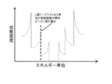
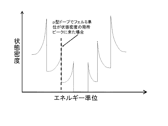
第1〜第4ナノワイヤ4〜7におけるドーパント量は、第1〜第4ナノワイヤ4〜7のフェルミ準位が状態密度のピークにあるように、又は状態密度のピーク近くにあるように調節すると好ましい。図3及び図4に、図1に示す熱電変換素子1のナノワイヤ4〜7を擬一次元構造とした場合の電子の状態密度の模式図を示す。図3に示す電子のエネルギー状態密度を見ると、一次元性のバンド分散を持つ材料では、あるエネルギー準位に対して状態密度にピークが生じる。この物質に不純物をドープすると、図4に示すように、そのドープ濃度に依存してフェルミ準位の位置が、状態密度が最大になった点を横切ることがしばしば生じる。n型ドープの場合には電子(p型ドープの場合には正孔)の状態密度が最大になった場所にフェルミ準位がある場合には、上記式2におけるゼーベック係数Sが1桁増大する。理想的な理論計算によると2桁増大させることも可能であるが、実際の材料ではフェルミ準位の状態密度が増大すると、自発的に半導体部分の結晶を構成する原子配置が変化して状態密度の増大が抑制されるので、増大は1桁におさまる。
It is preferable to adjust the dopant amount in the first to
半導体基材21へのドーパント22のドープ程度は、半導体基材21の表面に付着させるにとどめるようにすると好ましい。すなわち、ドーパント22を半導体基材21の内部に注入させないようにすると好ましい。また、ドーパント22は、半導体基材21の表面上において、周期性をもって配列しないようにすると好ましい。すなわち、ドーパント22を半導体基材21の表面にランダムに付着させると好ましい。
The degree of doping of the
第1〜第4ナノワイヤ4〜7において、ドーパント22が不規則的に付着しているかどうかは、第1〜第4ナノワイヤ4〜7の表面の電子線回折を測定することによって判断することができる。例えば、電子線回折の撮像スクリーンにパターンが検出されないと好ましい。この場合、ドーパント22が周期性無く半導体材料表面に付着していることが示される。したがって、ドーパント22は、電子線回折の撮像スクリーンにパターンが検出されないように半導体材料に付着させると好ましい。
In the first to
ドーパント22が半導体基材21の表面に付着したのみであっても、半導体基材21の幅はナノメートルオーダーであるので、キャリア(正孔又は電子)は、半導体基材21の内部にまで浸透することができる。これにより、第1〜第4ナノワイヤ4〜7は半導体の性質を有することになる。
Even if the
第1電極及び第2電極は導電性材料である。第1電極及び第2電極としては、例えば、アルミニウム、銅等を使用することができる。 The first electrode and the second electrode are conductive materials. As the first electrode and the second electrode, for example, aluminum, copper, or the like can be used.
高温部12及び低温部13は、ナノワイヤ4〜7及び半導体材料2〜3に温度勾配を所持させるものである。高温部12には例えば加熱装置(不図示)接続されている。低温部13には例えば冷却装置(不図示)が接続されている。高温部12及び低温部13は絶縁性材料であり、高温部12及び低温部13に電流が流れると起電力が失われてしまうので、高温部12及び低温部13はバンドギャップが大きい絶縁性材料であると好ましい。高温部12及び低温部13としては、例えば、SiO2等のガラス材料を用いることができる。
The high-
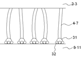
図5に、熱電変換素子におけるナノワイヤの拡大概略平面図を示す。熱電変換素子1は、第1〜第4電極8〜11と第1〜第4ナノワイヤ4〜7との間に介在する触媒31と、第1〜第4電極8〜11と第1〜第4ナノワイヤ4〜7とのコンタクト周囲に配された抵抗低下剤32と、をさらに備えると好ましい。
FIG. 5 shows an enlarged schematic plan view of nanowires in the thermoelectric conversion element. The
触媒31は、第1〜第4電極8〜11を成長させるために使用されるものである。触媒31としては、半導体材料を成長させる場合には、金、ニッケル、プラチナ、アルミニウム等の微粒子を使用することができる。カーボンナノチューブを成長させる場合には、鉄の微粒子を使用することができる。
The
抵抗低下剤32は、第1〜第4電極8〜11から第1〜第4ナノワイヤ4〜7へ電子・正孔を注入する際に、両者間の接触抵抗を減らして電子・正孔の伝導性を高めるものである。n型の第1電極8及び第2電極9における抵抗低下剤32としては、電子の注入を容易にする物質、例えばカリウム(K)やカルシウム(Ca)等の金属微粒子を使用することができる。p型の第3電極10及び第4電極11における抵抗低下剤32としては、正孔の注入を容易にする物質、例えばフラーレン、ペンタセン等を使用することができる。
The
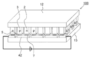
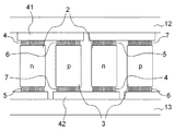
次に、本発明の第1実施形態に係る熱電変換モジュールについて説明する。図6に、本発明の第1実施形態に係る熱電変換モジュールの概略斜視図を示す。図7に、図6に示す熱電変換モジュールの概略部分平面図を示す。図6及び図7において、図1に示す要素と同じ要素には同じ符号を付してある。 Next, the thermoelectric conversion module according to the first embodiment of the present invention will be described. FIG. 6 shows a schematic perspective view of the thermoelectric conversion module according to the first embodiment of the present invention. FIG. 7 shows a schematic partial plan view of the thermoelectric conversion module shown in FIG. 6 and 7, the same elements as those shown in FIG. 1 are denoted by the same reference numerals.
熱電変換モジュール100は、基本的には、図1に示す熱電変換素子1を並列に配置した構成を有する。すなわち、第1ナノワイヤ4、n型半導体材料2及び第2ナノワイヤ5で構成されたn型ユニットと、第3ナノワイヤ6、p型半導体材料3及び第4ナノワイヤ7で構成されたp型ユニットと、は交互に配列されている。図1に示す熱電変換ユニット1においては各電極は隣接するユニット同士を電気的に接続していないが、熱電変換モジュール100においては、各電極は、隣接するユニット同士を電気的に接続している。第1電極41は、高温部12側においてn型ユニットとp型ユニットを電気的に接続している。すなわち、第1電極41は、第1ナノワイヤ4を介してn型半導体材料2と電気的に接続され、第3ナノワイヤ6を介してp型半導体材料3と電気的に接続されている。第2電極42は、低温部13側においてp型ユニットとn型ユニットを電気的に接続している。すなわち、第2電極42は、第4ナノワイヤを介してp型半導体材料3と電気的に接続され、第2ナノワイヤ5を介してn型半導体材料2と電気的に接続されている。第1電極41と第2電極42は互い違いに配列されている。すなわち、第1電極41と第2電極42とが同一のn型ユニットに接続されている場合には、その第1電極41と第2電極42とは異なるp型ユニットに接続されている。同様に、第1電極41と第2電極42とが同一のp型ユニットに接続されている場合には、その第1電極41と第2電極42とは異なるn型ユニットに接続されている。高温部12及び低温部13は、図1に示すように電極毎に設けてもよいが、図6及び図7に示す形態においては、高温部12は、複数の第1電極41に共通の基板として構成し、低温部13は、複数の第2電極42に共通の基板として構成している。
The
熱電変換モジュール100によれば、高密度実装が可能であり、取得電圧を高めることができる。
According to the
次に、本発明の第1実施形態に係る熱電変換素子の製造方法について説明する。図8に、本発明の第1実施形態に係る熱電変換素子の製造方法を説明するための概略工程図を示す。 Next, the manufacturing method of the thermoelectric conversion element which concerns on 1st Embodiment of this invention is demonstrated. In FIG. 8, the schematic process drawing for demonstrating the manufacturing method of the thermoelectric conversion element which concerns on 1st Embodiment of this invention is shown.
まず、第1〜第4電極8〜11を準備する。次に、各電極8〜11上に、ナノワイヤ4〜7の成長に必要な触媒31を配置する。次に、各電極8〜11上に、各電極8〜11からナノワイヤ4〜7を成長させる長さ程度離して半導体材料2〜3を配置する(図8(a))。
First, first to
次に、触媒31からナノワイヤ4〜7を成長させる。例えば、化学気相成長法(CVD(Chemical Vapor Deposition)法)やVLS(Vapor-Liquid-Solid)法などの技術を用いたガス噴き掛け33によりナノワイヤ4〜7を成長させる。この際、電界34を付加することでナノワイヤ4〜7の成長方向を制御する。成長したナノワイヤ4〜7は、半導体材料2〜3と接合ないし接触し、ナノワイヤ4〜7と半導体材料2〜3は電気的に接続される(図8(b))。ナノワイヤ4〜7は、半導体材料2〜3の両側同時に成長させてもよいし、片側ずつ成長させてもよい。
Next,
次に、電極8〜11とナノワイヤ4〜7との接合部の周囲に抵抗低下剤32を吸着させる(図8(c))。図8に示す形態においては、ナノワイヤ4〜7を成長させた後に抵抗低下剤32を付与したが、抵抗低下剤32を付与した後にナノワイヤ4〜7を成長させてもよい。
Next, the
次に、ナノワイヤ4〜7にドーパント22を吸着させる。図9に、ドーパントを吸着させる際の概略斜視図を示す。ナノワイヤ4〜7を介して電極8〜11と半導体材料2〜3とを接続したn型ユニットとp型ユニットとの間に隔離壁35を形成する。隔離壁35は、ナノワイヤ4〜7にドーパントを供給する際に、n型用のドーパントとp型用のドーパントの両方がナノワイヤに付着することを防止するものである。隔離壁35を形成した後、第1ナノワイヤ4及び第2ナノワイヤ5にn型用ドーパントを吸着させる工程と、第3ナノワイヤ6及び第4ナノワイヤ7にp型用ドーパントを吸着させる工程とを別々に実施する。隔離壁35を設けることにより、p型用ドーパントが第1ナノワイヤ4及び第2ナノワイヤ5に付着することを防止し、また、n型用ドーパントが第3ナノワイヤ6及び第4ナノワイヤ7に付着することを防止する。
Next, the
隔離壁35は、絶縁性を有すると共に、熱伝導性が低いものにすると好ましい。隔離壁35としては、ガラス材料や酸化シリコン等を使用することができる。これにより、例えば、図6のようなモジュールを作製する場合、熱電変換素子間の短絡を防止することができる。
The
ドーパントの吸着量は、半導体部分の光吸収測定を実施しながら、フェルミ準位を状態密度のピーク位置に合わせるように調節すると好ましい。擬一次元系のナノワイヤはその状態密度に一次元系に特有なピークを有する。ナノワイヤへの分子ドーパントの量をこの状態密度が最大ピークになる所に合わせるように導入することにより、電子・正孔の流れを大きくすることができ、キャリアの伝導性を向上させることが可能になる。したがって、ドーパント吸着量は、半導体部分の光吸収測定で、状態密度の占有部分のピーク位置から非占有部分へのピーク位置に移行する際に現れる光吸収ピークの消失により調整する。 The amount of adsorbed dopant is preferably adjusted so that the Fermi level matches the peak position of the state density while performing optical absorption measurement of the semiconductor portion. A quasi-one-dimensional nanowire has a peak specific to the one-dimensional system in the density of states. By introducing the amount of molecular dopant into the nanowire so that the density of states reaches the maximum peak, the flow of electrons and holes can be increased, and the conductivity of carriers can be improved. Become. Accordingly, the amount of adsorbed dopant is adjusted by the disappearance of the light absorption peak that appears when shifting from the peak position of the occupied portion of the state density to the peak position of the unoccupied portion in the light absorption measurement of the semiconductor portion.
上記製造方法によれば、熱電変換素子を簡易な方法で製造することができる。 According to the said manufacturing method, a thermoelectric conversion element can be manufactured by a simple method.
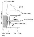
次に、本発明の第1実施形態に係る熱電変換素子1の作用について説明する。図10に、キャリアが電極からナノワイヤへと導入される模式図を示す。図10においては、電極8〜11の領域は、電極における電子状態を模式的に示している。電極8〜11とナノワイヤ4〜7との接合部の領域は、キャリアに対するエネルギー障壁を図示している。ナノワイヤ4〜7の領域は、エネルギーに対する状態密度を図示している。
Next, the operation of the
熱電変換素子1において発電するためには、第1電極8及び第3電極10を高温とし、第2電極9及び第4電極を第1電極8及び第3電極10よりも低温として、n型半導体材料2、p型半導体材料3及び第1〜第4ナノワイヤ4〜7において温度勾配を発生させる。これにより、電子と正孔のキャリア移動と熱拡散における熱伝導を生じさせる。
In order to generate electric power in the
熱電変換素子において熱伝導及び電子・正孔のキャリア移動度を阻害する原因の一つは、異種接合を要する電極と半導体材料との接合部である。特に、電極と半導体材料との接合部における電気抵抗を小さくし電気伝導度を大きくすることが重要である。そこで、本発明の熱電変換素子1においては、電極8〜11と半導体材料2〜3とをナノワイヤ4〜7で接合することにより、金属原子と半導体原子の原子拡散を抑制する。また、電極8〜11とナノワイヤ4〜7との接合部には、抵抗低下剤32を供給することにより、キャリア伝導性を高めている。すなわち、キャリアに対する接合部におけるエネルギー障壁を低くしている。
One of the causes of hindering heat conduction and electron / hole carrier mobility in a thermoelectric conversion element is a junction between an electrode and a semiconductor material that require heterojunction. In particular, it is important to reduce the electrical resistance and increase the electrical conductivity at the junction between the electrode and the semiconductor material. Therefore, in the
さらに、ナノワイヤ4〜7は、半導体基材21の表面にドーパント22が付着することにより、半導体ナノワイヤを形成し、表面吸着分子とのフォノン散乱効果により熱伝導を小さくしている。すなわち、ナノワイヤ4〜7は、電極8〜11から半導体材料2〜3への熱伝導性を低下させている。
Furthermore, the
電子・正孔によるキャリア伝導に関して、電子や正孔のエネルギーバンド数が伝導帯と価電子帯で少なくなるが、電子・正孔の波数変化に対するエネルギー変化(バンド分散)がフォノンのバンド分散よりも大きいため、次元の低下に対してキャリア伝導度の低下は小さい。ドーパント22を半導体基材21の表面に付着させるにとどめると、キャリアを放出し、帯電したドーパント22は、半導体基材21の表面のみに存在することになる。これにより、帯電したドーパント22が電子及び正孔の移動23を阻害する影響を低減することができる。すなわち、半導体基材21内部における電子及び正孔の移動度は、表面に存在する帯電したドーパント22によって低減されにくくなる。よって、電子・正孔のキャリア伝導度で決まるゼーベック係数Sは大きく低下しない。
Regarding the carrier conduction by electrons and holes, the energy band number of electrons and holes decreases in the conduction band and valence band, but the energy change (band dispersion) with respect to the wave number change of electrons and holes is more than the band dispersion of phonons. Because it is large, the decrease in carrier conductivity is small with respect to the decrease in dimension. If the
熱伝導に関して、擬一次元構造の第1〜第4ナノワイヤ4〜7においては、第1〜第4ナノワイヤ4〜7の直径が小さくなるにつれ、熱伝導率κ(上記式2)が大きく低下し、その結果として熱電性能指数ZTが大きく増大する(非特許文献3参照)。ここで、擬一次元構造で熱伝導率κが下がる理由は、熱の伝播を担う媒体である材料の格子振動の振動モードが少なくなるために、熱伝導のフォノンが少なくなるためである。
Regarding the heat conduction, in the first to
フォノン伝導は第1〜第4ナノワイヤ4〜7表面の構造変化や乱れに大きく影響を受けて伝導が低下する。熱の伝導を担う音響フォノンは、図2に示す矢印24のように、第1〜第4ナノワイヤ4〜7の外面を伝播する。一般に、n型ドーパントである分子又はp型ドーパントである分子を、図4に示すようにフェルミ準位が状態密度のピーク位置にまで変化するまでの量を付着させると、一次元の長手方向50Åの範囲に、概算で平均一個の分子が付着されていることになる。音響フォノンは清浄表面では通常の材料で1000Åの距離を弾道的にすすむことが出来るが、その弾道距離が50Åに縮むので、伝導度κは約20分の1に低下すると概算見積もりすることができる。したがって、第1〜第4ナノワイヤ4〜7の表面に不規則にドーパント22が付着していると、格子のなす周期的構造が乱されるので、音響フォノンが散乱され、伝播速度が著しく低下することになる。
Phonon conduction is greatly affected by structural changes and disturbances on the surfaces of the first to
以上より、第1〜第4ナノワイヤ4〜7により熱電変換効率を増大させることができる。
From the above, the thermoelectric conversion efficiency can be increased by the first to
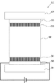
次に、本発明の第2実施形態に係る熱電変換素子について説明する。図11に、本発明の第2実施形態に係る熱電変換素子の概略平面図を示す。 Next, a thermoelectric conversion element according to the second embodiment of the present invention will be described. In FIG. 11, the schematic plan view of the thermoelectric conversion element which concerns on 2nd Embodiment of this invention is shown.
第2実施形態に係る熱電変換素子51は、磁性体52と、磁性体52の一方の端部に磁気的に接続された第1ナノワイヤ53と、磁性体52の他方の端部に磁気的に接続された第2ナノワイヤ54と、第1ナノワイヤ53と磁気的に接続された第1電極55と、第2ナノワイヤ54と磁気的に接続された第2電極56と、第1電極55と熱的に接続された高温部57と、第2電極56と熱的に接続された低温部58と、を備える。磁性体52と第1電極55とは、第1ナノワイヤ53を介して磁気的に接続される。磁性体52と第2電極56とは、第2ナノワイヤ54を介して磁気的に接続される。
The
本発明において、磁気的に接続されているとは、スピン間相互作用を有することをいう。また、本発明において、磁性とは、スピン間相互作用によってスピン配列に秩序を有する性質をいう。 In the present invention, being magnetically connected means having an interaction between spins. In the present invention, magnetism refers to the property of ordering in the spin arrangement due to the interaction between spins.
磁性体52は、熱伝導性の低い材料、例えば絶縁体であると好ましい。磁性体52としては、強磁性体(フェロ磁性体)やフェリ磁性体を使用することができ、熱伝導率の小さく、かつスピン流の緩和が小さな材料を用いることが望ましい。磁性体52として、例えば、ガーネットフェライトやスピネルフェライトなどの酸化物系の磁性体を用いることができる。特に、多結晶やナノ結晶の磁性体52材料を用いれば、効果的なフォノン散乱によってフォノン熱伝導を抑制し、さらに高い感度・分解能を得ることが可能となる。
The
第1電極55及び第2電極56は、逆スピンホール効果によってスピン流から熱起電力を取り出すために、スピン軌道相互作用を有する材料を含有するものが好ましい。電極55,56として、例えば、スピン軌道相互作用の比較的大きなAu、Pt、Pdなどの金属材料、又はこのような金属材料を含有する合金材料を用いることができる。電極55,56は、逆スピンホール効果を強めるために、FeやCuなどの不純物を含有してもよい。電極55,56の厚さは、スピン流を高い効率で電気に変換するために、少なくとも金属材料のスピン拡散長以上に設定すると好ましい。例えば、電極をAuで形成する場合、電極の厚さは50nm以上に設定すると好ましく、Ptで形成する場合、厚さは10nm以上に設定するのと好ましい。
The
第1ナノワイヤ53及び第2ナノワイヤ54は磁性体である。第1ナノワイヤ53及び第2ナノワイヤ54は、少なくとも一方向の磁化を有する磁性材料、例えば強磁性体(フェロ磁性体)やフェリ磁性体を含有する。ナノワイヤ53,54としては、例えば、鉄やニッケルなどの金属材料や、スピネルフェライトなどの絶縁体材料を用いることができる。
The
ナノワイヤ53,54は、線状構造(擬一次元構造)を有する。例えば、ナノワイヤ53,54の長さは、100ナノメートル〜1000ナノメートルであると好ましい。ナノワイヤ53,54の太さは、マグノンの伝播経路を確保することができる太さ、例えば、1ナノメートル以上100ナノメートル以下であると好ましく、1ナノメートル以上10ナノメートル以下であるとより好ましい。
The
ナノワイヤ53,54と電極55,56との接合部には、スピンの伝導率を高める抵抗低下剤を付与してもよい。
A resistance lowering agent that increases the spin conductivity may be applied to the junction between the
次に、本発明の第2実施形態に係る熱電変換素子の製造方法について説明する。図12に、本発明の第2実施形態に係る熱電変換素子の製造方法を説明するための概略工程図を示す。 Next, the manufacturing method of the thermoelectric conversion element which concerns on 2nd Embodiment of this invention is demonstrated. In FIG. 12, the schematic process drawing for demonstrating the manufacturing method of the thermoelectric conversion element which concerns on 2nd Embodiment of this invention is shown.
まず、熱電変換素子を支える基板61を準備する。例えば、厚さ0.5mmのガドリニウムガリウムガーネット(以下、「GGG」という。)基板を用いることができる。
First, a
次に、基板61上に磁性体52を形成する。磁性体52は、例えば、有機金属堆積法(MOD(Metal Organic Deposition)法)、ゾルゲル法、エアロゾルデポジション法(AD(Aerosol Deposition)法)などの方法により形成することができる。塗布・印刷ベースの成膜法を用いれば、大面積基板にも一括成膜することが可能で、生産性の高い製造が可能となる。例えば、GGG基板上に、イットリウム(Y)サイトの一部をBiで置換したイットリウム鉄ガーネット(組成BiY2Fe5O12。以下、「Bi−YIG」という。)を含有する磁性体52をエアロゾルデポジション法により堆積することができる。Bi−YIG原料には、直径300nmのBi−YIG微粒子を用いることができる。このBi−YIG微粒子をエアロゾル発生容器に詰めておき、GGG基板は成膜チャンバ内のホルダーに固定する。この状態で成膜チャンバとエアロゾル発生容器との間に圧力差を生じさせることで、Bi−YIG微粒子が成膜チャンバ内へと引き込まれ、ノズルを通してGGG基板上に吹き付けられる。このときの基板での衝突エネルギーによって微粒子が粉砕・再結合し、GGG基板上にBi−YIG多結晶が形成される。基板ステージを2次元的にスキャンすることで、基板上に均一なBi−YIG磁性体52層を例えば膜厚0.1mmで成膜することができる。
Next, the
ナノワイヤ53,54は、例えば、電気化学的方法、適切な条件下での熱酸化等によって作製することができる。
The
電極55,56は、スパッタ法や蒸着法等の方法で作製することができる。また、インクジェット法やスクリーン印刷法のような生産性の高い製造方法で作製することもできる。
The
例えば、Bi−YIG52の表面を研磨した後、最初に、ナノワイヤの前駆層62となる膜厚1μmのFe層を、Bi−YIG52上にスパッタ法により成膜する。次に、電極55,56となる膜厚30nmのPt層をFe層62上にスパッタ法により成膜する。次に、これらを酸素雰囲気化において500℃の高温で5時間アニールすることで、Fe層の酸化、およびナノ構造化が進行し、Bi−YIGとPt層との間に直径50nm、長さ1μmの多数のヘマタイト(α−Fe2O3)ナノワイヤ53,54を形成することができる。ナノワイヤの前駆層62を磁性体52の両端に形成した後に熱酸化してもよいし、磁性体52の片側ずつナノワイヤ53,54を形成してもよい。
For example, after polishing the surface of the Bi-YIG 52, an Fe layer having a thickness of 1 μm to be the
上記方法によれば、磁気的に接続された磁性材料であるナノワイヤを容易に作製することができる。 According to the above method, nanowires that are magnetically connected magnetic materials can be easily produced.
次に、本発明の第2実施形態に係る熱電変換素子51の作用について説明する。熱電変換素子51においては、スピン流によるスピンゼーベック効果により起電力を発生させる。このスピン流によるゼーベック効果においては、磁性体52及びナノワイヤ53,54を流れる上向きスピン及び下向きスピンが第1実施形態におけるn型半導体材料の電子とp型半導体材料の正孔に対応している。スピン流は電極55,56内でスピン・軌道相互作用を用いた逆スピンホール効果により電子系に変換される。スピン流は平均自由行程が1cm近くと極めて大きく、散乱や緩和を伴わないために磁性体52では発熱が起きない。従って、熱電変換効率を高くする要素としては、高温部57と低温部58との温度差を保つために電極55,56及び磁性体52を流れるフォノンによる熱伝導を下げることが挙げられる。そこで、熱電変換素子51においては、電極55,56と磁性体52との間にナノワイヤ53,54を形成することにより、フォノン伝導を抑制している。すなわち、ナノワイヤ53,54が磁性材料である場合、スピン伝導はスピンチャネルを通して大きく散乱されることなく透過する。これにより、ナノワイヤ53,54を電極55,56と磁性体52との間に形成することにより熱電変換効率を高めることが可能になる。
Next, the operation of the
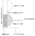
図13に、スピン流が電極からナノワイヤへ導入される際の模式図を示す。ナノワイヤ53,54においては、スピン発生の元となる電子間のクーロン反発相互作用により、上向きスピンが通過する伝導帯(上部ハバード帯)と下向きスピンが通過する伝導帯(下部ハバード帯)がそれぞれ分裂している。電極の状態密度とナノワイヤの伝導帯の状態密度の重なりを大きくすることができれば、スピン流の伝導性を向上させることが可能となる。
FIG. 13 shows a schematic diagram when the spin current is introduced from the electrode to the nanowire. In the
また、ナノワイヤ53,54は、第1実施形態と同様にして、電極55,56と磁性体52間の熱伝導性を低下させることにより、熱電変換効率を高めている。
The
本実施形態によれば、第1実施形態と異なり、n型ユニットとp型ユニットのように2種類の基本素子を必要としない。これにより、所要面積に対して効率よく熱電変換素子を形成することができる。また、発電量を高める場合には、図6に示す熱電変換モジュールのように複数の熱電変換素子を組み合わせる必要がなく大面積化が容易であり、電極と磁性体の接合面積を大きくするだけで発電量を高めることができる。 According to the present embodiment, unlike the first embodiment, two types of basic elements are not required unlike the n-type unit and the p-type unit. Thereby, a thermoelectric conversion element can be efficiently formed with respect to a required area. In addition, when the amount of power generation is increased, it is not necessary to combine a plurality of thermoelectric conversion elements as in the thermoelectric conversion module shown in FIG. 6, and it is easy to increase the area, and only the junction area between the electrode and the magnetic material is increased. The amount of power generation can be increased.
本発明の熱電変換素子及びその製造方法は、上記実施形態に基づいて説明されているが、上記実施形態に限定されることなく、本発明の範囲内において、かつ本発明の基本的技術思想に基づいて、上記実施形態に対し種々の変形、変更及び改良を含むことができることはいうまでもない。また、本発明の請求の範囲の枠内において、種々の開示要素の多様な組み合わせ・置換ないし選択が可能である。 The thermoelectric conversion element and the manufacturing method thereof according to the present invention have been described based on the above embodiment, but are not limited to the above embodiment, and are within the scope of the present invention and within the basic technical idea of the present invention. It goes without saying that various modifications, changes and improvements can be included in the above embodiment. Further, various combinations, substitutions, or selections of various disclosed elements are possible within the scope of the claims of the present invention.
本発明のさらなる課題、目的及び展開形態は、請求の範囲を含む本発明の全開示事項からも明らかにされる。 Further problems, objects, and developments of the present invention will become apparent from the entire disclosure of the present invention including the claims.
上記実施形態の一部又は全部は、以下の付記のようにも記載されうるが、以下の記載には限定されない。 A part or all of the above embodiment may be described as in the following supplementary notes, but is not limited to the following description.
(付記1)
熱電変換材料である半導体材料と、
前記半導体材料に電気的に接続された少なくとも1つのナノワイヤと、
前記ナノワイヤと電気的に接続された電極と、を備え、
前記ナノワイヤは、半導体基材と、前記半導体基材の表面に付着したドーパントと、を有することを特徴とする熱電変換素子。
(Appendix 1)
A semiconductor material that is a thermoelectric conversion material;
At least one nanowire electrically connected to the semiconductor material;
An electrode electrically connected to the nanowire,
The nanowire includes a semiconductor base material and a dopant attached to the surface of the semiconductor base material.
(付記2)
前記ナノワイヤと前記電極との接合部に、前記ナノワイヤと前記電極との電気抵抗を低下させる抵抗低下剤をさらに備えることを特徴とする付記1に記載の熱電変換素子。
(Appendix 2)
The thermoelectric conversion element according to
(付記3)
前記半導体材料としてn型半導体材料と、p型半導体材料と、を備え、
前記ナノワイヤとして、前記n型半導体材料の一方の端部と電気的に接続された少なくとも1つの第1ナノワイヤと、前記n型半導体材料の他方の端部と電気的に接続された少なくとも1つの第2ナノワイヤと、前記p型半導体材料の一方の端部と電気的に接続された少なくとも1つの第3ナノワイヤと、前記p型半導体材料の他方の端部と電気的に接続された少なくとも1つの第4ナノワイヤと、を備え、
前記電極として、前記第1ナノワイヤと電気的に接続された第1電極と、前記第2ナノワイヤと電気的に接続された第2電極と、前記第3ナノワイヤと電気的に接続された第3電極と、前記第4ナノワイヤと電気的に接続された第4電極と、を備えることを特徴とする付記1又は2に記載の熱電変換素子。
(Appendix 3)
An n-type semiconductor material and a p-type semiconductor material as the semiconductor material,
As the nanowire, at least one first nanowire electrically connected to one end of the n-type semiconductor material, and at least one first wire electrically connected to the other end of the n-type semiconductor material. Two nanowires, at least one third nanowire electrically connected to one end of the p-type semiconductor material, and at least one first electrically connected to the other end of the p-type semiconductor material. 4 nanowires,
As the electrodes, a first electrode electrically connected to the first nanowire, a second electrode electrically connected to the second nanowire, and a third electrode electrically connected to the third nanowire And a fourth electrode electrically connected to the fourth nanowire. The thermoelectric conversion element according to
(付記4)
前記第1ナノワイヤと前記第1電極との接合部及び前記第2ナノワイヤと前記第2電極との接合部に、前記第1ナノワイヤと前記第1電極との電気抵抗及び前記第2ナノワイヤと前記第2電極との電気抵抗を低下させる抵抗低下剤をさらに備え、
前記抵抗低下剤は、カルシウム及びカリウムのうち少なくとも一方を含有することを特徴とする付記3に記載の熱電変換素子。
(Appendix 4)
The junction between the first nanowire and the first electrode and the junction between the second nanowire and the second electrode have an electrical resistance between the first nanowire and the first electrode, and the second nanowire and the first electrode. It further comprises a resistance reducing agent that reduces the electrical resistance with the two electrodes,
The thermoelectric conversion element according to
(付記5)
前記第3ナノワイヤと前記第3電極との接合部及び前記第4ナノワイヤと前記第4電極との接合部に、記第3ナノワイヤと前記第3電極との電気抵抗及び前記第4ナノワイヤと前記第4電極との電気抵抗を低下させる抵抗低下剤をさらに備え、
前記抵抗低下剤は、フラーレン及びペンタセンのうち少なくとも一方を含有することを特徴とする付記3又は4に記載の熱電変換素子。
(Appendix 5)
The junction between the third nanowire and the third electrode and the junction between the fourth nanowire and the fourth electrode are connected to the electrical resistance of the third nanowire and the third electrode, and the fourth nanowire and the fourth electrode. A resistance reducing agent that lowers the electrical resistance with the four electrodes;
The thermoelectric conversion element according to
(付記6)
各ナノワイヤのフェルミ準位が状態密度のピークにあることを特徴とする付記1〜5のいずれか一項に記載の熱電変換素子。
(Appendix 6)
The thermoelectric conversion element according to any one of
(付記7)
各ナノワイヤは、キャリアの伝導方向が擬一次元方向となるような構造を有することを特徴とする付記1〜6のいずれか一項に記載の熱電変換素子。
(Appendix 7)
Each nanowire has a structure in which the carrier conduction direction becomes a quasi-one-dimensional direction, The thermoelectric conversion element according to any one of
(付記8)
異なる導電型の前記ナノワイヤ間及び前記半導体材料間に隔離壁をさらに備えることを特徴とする付記1〜7のいずれか一項に記載の熱電変換素子。
(Appendix 8)
The thermoelectric conversion element according to any one of
(付記9)
絶縁性を有する磁性体と、
前記磁性体と磁気的に接続された磁性材料を含有する少なくとも1つのナノワイヤと、
前記ナノワイヤと磁気的に接続された電極と、
を備えることを特徴とする熱電変換素子。
(Appendix 9)
An insulating magnetic material;
At least one nanowire containing a magnetic material magnetically connected to the magnetic body;
An electrode magnetically connected to the nanowire;
A thermoelectric conversion element comprising:
(付記10)
前記ナノワイヤとして、前記磁性体の一方の端部と磁気的に接続された少なくとも1つの第1ナノワイヤと、前記磁性体の他方の端部と磁気的に接続された少なくとも1つの第2ナノワイヤと、を備え、
前記電極として、前記第1ナノワイヤと磁気的に接続された第1電極と、前記第2ナノワイヤと磁気的に接続された第2電極と、を備えることを特徴とする付記9に記載の熱電変換素子。
(Appendix 10)
As the nanowire, at least one first nanowire magnetically connected to one end of the magnetic body, and at least one second nanowire magnetically connected to the other end of the magnetic body, With
The thermoelectric conversion according to
(付記11)
各ナノワイヤは、スピンの伝導方向が擬一次元方向となるような構造を有することを特徴とする付記9又は10に記載の熱電変換素子。
(Appendix 11)
The thermoelectric conversion element according to
(付記12)
各ナノワイヤの太さは、1ナノメートル〜1000ナノメートルであることを特徴とする付記1〜11のいずれか一項に記載の熱電変換素子。
(Appendix 12)
The thickness of each nanowire is 1 nanometer-1000 nanometer, The thermoelectric conversion element as described in any one of the supplementary notes 1-11 characterized by the above-mentioned.
(付記13)
付記1〜12のいずれか一項に記載の熱電変換素子を複数配列したことを特徴とする熱電変換モジュール。
(Appendix 13)
A thermoelectric conversion module, wherein a plurality of the thermoelectric conversion elements according to any one of
(付記14)
少なくとも1つの隣接する1対の熱電変換素子間において、少なくとも一方の電極を共有していることを特徴とする付記13に記載の熱電変換モジュール。
(Appendix 14)
14. The thermoelectric conversion module according to
(付記15)
電極上に触媒を供給する工程と、
前記電極の上方に半導体材料を配置する工程と、工程と、
ナノワイヤの先端が前記半導体材料に接合又は接触するように、前記触媒から前記ナノワイヤを成長させる工程と、
前記ナノワイヤの表面にドーパントを付着させる工程と、
を含むことを特徴とする熱電変換素子の製造方法。
(Appendix 15)
Supplying a catalyst on the electrode;
Disposing a semiconductor material above the electrode; and
Growing the nanowire from the catalyst such that the tip of the nanowire is bonded or in contact with the semiconductor material;
Attaching a dopant to the surface of the nanowire;
The manufacturing method of the thermoelectric conversion element characterized by including this.
(付記16)
前記ナノワイヤと前記電極との接合部に、前記ナノワイヤと前記電極との電気抵抗を低下させる抵抗低下剤を供給する工程をさらに含むことを特徴とする付記15に記載の熱電変換素子の製造方法。
(Appendix 16)
The method of manufacturing a thermoelectric conversion element according to appendix 15, further comprising a step of supplying a resistance lowering agent that lowers an electrical resistance between the nanowire and the electrode to a joint between the nanowire and the electrode.
(付記17)
異なるドーパントを供給するナノワイヤ間に隔離壁を形成する工程をさらに含むことを特徴とする付記15又は16に記載の熱電変換素子の製造方法。
(Appendix 17)
The method for producing a thermoelectric conversion element according to appendix 15 or 16, further comprising a step of forming an isolation wall between nanowires supplying different dopants.
(付記18)
前記隔離壁は絶縁性を有することを特徴とする付記17に記載の熱電変換素子の製造方法。
(Appendix 18)
18. The method for manufacturing a thermoelectric conversion element according to appendix 17, wherein the isolation wall has an insulating property.
(付記19)
前記ナノワイヤの表面にドーパントを付着させる工程において、
フェルミ準位が状態密度のピーク位置となるようにドーパントを付着させることを特徴とする付記15〜18のいずれか一項に記載の熱電変換素子の製造方法。
(Appendix 19)
In the step of attaching a dopant to the surface of the nanowire,
The method for producing a thermoelectric conversion element according to any one of appendices 15 to 18, wherein the dopant is attached so that the Fermi level is a peak position of the state density.
(付記20)
磁性体を形成する工程と、
前記磁性体上にナノワイヤ前駆層を形成する工程と、
前記ナノワイヤ前駆層上に電極を形成する工程と、
前記ナノワイヤ前駆層を酸化させて、少なくとも1つのナノワイヤを形成する工程と、
を含むことを特徴とする熱電変換素子の製造方法。
(Appendix 20)
Forming a magnetic material;
Forming a nanowire precursor layer on the magnetic material;
Forming an electrode on the nanowire precursor layer;
Oxidizing the nanowire precursor layer to form at least one nanowire;
The manufacturing method of the thermoelectric conversion element characterized by including this.
本発明の熱電変換素子及び熱電変換モジュールは、例えば、パソコン、携帯電話等の電子機器から排出される廃熱の電源への再利用、ウェアラブルな電子機器やセンサーへの給電素子、夜間の太陽電池を補完する予備電源、寒冷地での屋内外の温度差を利用したヒーター、高熱を発生させるリチウム電池電気系統における熱電変換装置として利用することができる。 The thermoelectric conversion element and the thermoelectric conversion module of the present invention can be reused, for example, as a power source for waste heat discharged from electronic devices such as personal computers and mobile phones, power supply elements for wearable electronic devices and sensors, and nighttime solar cells. It can be used as a standby power source that complements the above, a heater that uses a temperature difference between indoor and outdoor in a cold region, and a thermoelectric conversion device in a lithium battery electrical system that generates high heat.
1 熱電変換素子
2 n型半導体材料
3 p型半導体材料
4〜7 第1〜第4ナノワイヤ
8〜11 第1〜第4電極
12 高温部
13 低温部
21 半導体基材
21a 表面欠陥・乱れ
22 ドーパント
23 電子又は正孔の流れ
24 フォノンの流れ
31 触媒
32 抵抗低下剤
33 ガス流
34 電界
35 隔離壁
41 第1電極
42 第2電極
51 熱電変換素子
52 磁性体
53,54 第1〜第2ナノワイヤ
55,56 第1〜第2電極
57 高温部
58 低温部
61 基板
62 ナノワイヤ前駆層
100 熱電変換モジュール
DESCRIPTION OF
Claims (10)
前記半導体材料に電気的に接続された少なくとも1つのナノワイヤと、
前記ナノワイヤと電気的に接続された電極と、を備え、
前記ナノワイヤは、半導体基材と、前記半導体基材の表面に付着したドーパントと、を有することを特徴とする熱電変換素子。 A semiconductor material that is a thermoelectric conversion material;
At least one nanowire electrically connected to the semiconductor material;
An electrode electrically connected to the nanowire,
The nanowire includes a semiconductor base material and a dopant attached to the surface of the semiconductor base material.
前記ナノワイヤとして、前記n型半導体材料の一方の端部と電気的に接続された少なくとも1つの第1ナノワイヤと、前記n型半導体材料の他方の端部と電気的に接続された少なくとも1つの第2ナノワイヤと、前記p型半導体材料の一方の端部と電気的に接続された少なくとも1つの第3ナノワイヤと、前記p型半導体材料の他方の端部と電気的に接続された少なくとも1つの第4ナノワイヤと、を備え、
前記電極として、前記第1ナノワイヤと電気的に接続された第1電極と、前記第2ナノワイヤと電気的に接続された第2電極と、前記第3ナノワイヤと電気的に接続された第3電極と、前記第4ナノワイヤと電気的に接続された第4電極と、を備えることを特徴とする請求項1又は2に記載の熱電変換素子。 An n-type semiconductor material and a p-type semiconductor material as the semiconductor material,
As the nanowire, at least one first nanowire electrically connected to one end of the n-type semiconductor material, and at least one first wire electrically connected to the other end of the n-type semiconductor material. Two nanowires, at least one third nanowire electrically connected to one end of the p-type semiconductor material, and at least one first electrically connected to the other end of the p-type semiconductor material. 4 nanowires,
As the electrodes, a first electrode electrically connected to the first nanowire, a second electrode electrically connected to the second nanowire, and a third electrode electrically connected to the third nanowire The thermoelectric conversion element according to claim 1, further comprising: a fourth electrode electrically connected to the fourth nanowire.
前記磁性体と磁気的に接続された磁性材料を含有する少なくとも1つのナノワイヤと、
前記ナノワイヤと磁気的に接続された電極と、
を備えることを特徴とする熱電変換素子。 An insulating magnetic material;
At least one nanowire containing a magnetic material magnetically connected to the magnetic body;
An electrode magnetically connected to the nanowire;
A thermoelectric conversion element comprising:
前記電極として、前記第1ナノワイヤと磁気的に接続された第1電極と、前記第2ナノワイヤと磁気的に接続された第2電極と、を備えることを特徴とする請求項4に記載の熱電変換素子。 As the nanowire, at least one first nanowire magnetically connected to one end of the magnetic body, and at least one second nanowire magnetically connected to the other end of the magnetic body, With
5. The thermoelectric device according to claim 4, comprising a first electrode magnetically connected to the first nanowire and a second electrode magnetically connected to the second nanowire as the electrodes. Conversion element.
前記電極の上方に半導体材料を配置する工程と、
ナノワイヤの先端が前記半導体材料に接合又は接触するように、前記触媒から前記ナノワイヤを成長させる工程と、
前記ナノワイヤの表面にドーパントを付着させる工程と、
を含むことを特徴とする熱電変換素子の製造方法。 Supplying a catalyst on the electrode;
Disposing a semiconductor material above the electrodes;
Growing the nanowire from the catalyst such that the tip of the nanowire is bonded or in contact with the semiconductor material;
Attaching a dopant to the surface of the nanowire;
The manufacturing method of the thermoelectric conversion element characterized by including this.
フェルミ準位が状態密度のピーク位置となるようにドーパントを付着させることを特徴とする請求項7又は8に記載の熱電変換素子の製造方法。 In the step of attaching a dopant to the surface of the nanowire,
The method of manufacturing a thermoelectric conversion element according to claim 7 or 8, wherein the dopant is attached so that the Fermi level is a peak position of the state density.
前記磁性体上にナノワイヤ前駆層を形成する工程と、
前記ナノワイヤ前駆層上に電極を形成する工程と、
前記ナノワイヤ前駆層を酸化させて、少なくとも1つのナノワイヤを形成する工程と、
を含むことを特徴とする熱電変換素子の製造方法。 Forming a magnetic material;
Forming a nanowire precursor layer on the magnetic material;
Forming an electrode on the nanowire precursor layer;
Oxidizing the nanowire precursor layer to form at least one nanowire;
The manufacturing method of the thermoelectric conversion element characterized by including this.
Priority Applications (1)
| Application Number | Priority Date | Filing Date | Title |
|---|---|---|---|
| JP2011124262A JP2012253178A (en) | 2011-06-02 | 2011-06-02 | Thermoelectric conversion element, method for manufacturing the same, and thermoelectric conversion module |
Applications Claiming Priority (1)
| Application Number | Priority Date | Filing Date | Title |
|---|---|---|---|
| JP2011124262A JP2012253178A (en) | 2011-06-02 | 2011-06-02 | Thermoelectric conversion element, method for manufacturing the same, and thermoelectric conversion module |
Publications (1)
| Publication Number | Publication Date |
|---|---|
| JP2012253178A true JP2012253178A (en) | 2012-12-20 |
Family
ID=47525730
Family Applications (1)
| Application Number | Title | Priority Date | Filing Date |
|---|---|---|---|
| JP2011124262A Withdrawn JP2012253178A (en) | 2011-06-02 | 2011-06-02 | Thermoelectric conversion element, method for manufacturing the same, and thermoelectric conversion module |
Country Status (1)
| Country | Link |
|---|---|
| JP (1) | JP2012253178A (en) |
Cited By (5)
| Publication number | Priority date | Publication date | Assignee | Title |
|---|---|---|---|---|
| JP2014154850A (en) * | 2013-02-13 | 2014-08-25 | Nec Corp | Thermoelectric conversion element and method of manufacturing the same |
| JP2015195359A (en) * | 2014-03-28 | 2015-11-05 | トヨタ自動車株式会社 | Phonon scattering material, nanocomposite thermoelectric material, and method of producing the same |
| JP2016015361A (en) * | 2014-07-01 | 2016-01-28 | 公立大学法人首都大学東京 | Semiconductor element manufacturing method and device, semiconductor element and thermoelectric transducer using the same |
| WO2017123057A1 (en) * | 2016-01-13 | 2017-07-20 | 엘지이노텍 주식회사 | Thermoelectric element |
| US11245061B2 (en) | 2019-04-26 | 2022-02-08 | Korea Institute Of Science And Technology | Thermoelectric device having a separate interlayer disposed between a thermoelectric leg and an electrode to reduce the contact resistance therebetween |
-
2011
- 2011-06-02 JP JP2011124262A patent/JP2012253178A/en not_active Withdrawn
Cited By (6)
| Publication number | Priority date | Publication date | Assignee | Title |
|---|---|---|---|---|
| JP2014154850A (en) * | 2013-02-13 | 2014-08-25 | Nec Corp | Thermoelectric conversion element and method of manufacturing the same |
| JP2015195359A (en) * | 2014-03-28 | 2015-11-05 | トヨタ自動車株式会社 | Phonon scattering material, nanocomposite thermoelectric material, and method of producing the same |
| JP2016015361A (en) * | 2014-07-01 | 2016-01-28 | 公立大学法人首都大学東京 | Semiconductor element manufacturing method and device, semiconductor element and thermoelectric transducer using the same |
| WO2017123057A1 (en) * | 2016-01-13 | 2017-07-20 | 엘지이노텍 주식회사 | Thermoelectric element |
| US10910541B2 (en) | 2016-01-13 | 2021-02-02 | Lg Innotek Co., Ltd. | Thermoelectric element |
| US11245061B2 (en) | 2019-04-26 | 2022-02-08 | Korea Institute Of Science And Technology | Thermoelectric device having a separate interlayer disposed between a thermoelectric leg and an electrode to reduce the contact resistance therebetween |
Similar Documents
| Publication | Publication Date | Title |
|---|---|---|
| Glavin et al. | Emerging applications of elemental 2D materials | |
| Zong et al. | Graphene-based thermoelectrics | |
| Li et al. | Intercalation strategy in 2D materials for electronics and optoelectronics | |
| Shi | Thermal and thermoelectric transport in nanostructures and low-dimensional systems | |
| Xu et al. | Integrated multilayer nanogenerator fabricated using paired nanotip-to-nanowire brushes | |
| Wu et al. | Large thermoelectricity via variable range hopping in chemical vapor deposition grown single-layer MoS2 | |
| Liang et al. | Thermoelectric properties of p-type PbSe nanowires | |
| Abramson et al. | Fabrication and characterization of a nanowire/polymer-based nanocomposite for a prototype thermoelectric device | |
| Liang et al. | Magnetotransport in Co-doped ZnO nanowires | |
| KR101956278B1 (en) | Heterogeneous laminate comprising graphene, thermoelectric material, thermoelectric module and thermoelectric apparatus comprising same | |
| Jaiswal et al. | Fe-doped armchair graphene nanoribbons for spintronic/interconnect applications | |
| CN104779275B (en) | Autoexcitation spin single electron Electromagnetic Environmental Effect transistor, preparation method and application | |
| KR101482598B1 (en) | Thermoelectric material, method for producing same, and thermoelectric conversion module using same | |
| Teweldebrhan et al. | Exfoliation and characterization of bismuth telluride atomic quintuples and quasi-two-dimensional crystals | |
| Ratnikov et al. | Two-dimensional graphene electronics: current status and prospects | |
| JPWO2012169509A1 (en) | Thermoelectric conversion element | |
| Sim et al. | Power factor enhancement for few-layered graphene films by molecular attachments | |
| JP2012089604A (en) | Thermoelectric conversion device, method of manufacturing the same, and thermoelectric conversion unit | |
| Hung et al. | Orientation-dependent room-temperature ferromagnetism of fesi nanowires and applications in nonvolatile memory devices | |
| Yan et al. | Morphology control of indium germanate nanowires, nanoribbons, and hierarchical nanostructures | |
| Ghasemzadeh et al. | Thermal spin filtering and spin-dependent Seebeck effect in α-borophene nanoribbons | |
| US20140373891A1 (en) | Thermoelectric structure, and thermoelectric device and thermoelectric apparatus including the same | |
| Wei et al. | The synthesis of Bi2Te3 nanobelts by vapor–liquid–solid method and their electrical transport properties | |
| Dresselhaus et al. | Advances in 1D and 2D thermoelectric materials | |
| Dai et al. | Recent Progress of Mechanical Exfoliation and the Application in the Study of 2 D Materials |
Legal Events
| Date | Code | Title | Description |
|---|---|---|---|
| A300 | Application deemed to be withdrawn because no request for examination was validly filed |
Free format text: JAPANESE INTERMEDIATE CODE: A300 Effective date: 20140805 |