JP2012256705A - 半導体装置の製造方法 - Google Patents
半導体装置の製造方法 Download PDFInfo
- Publication number
- JP2012256705A JP2012256705A JP2011128649A JP2011128649A JP2012256705A JP 2012256705 A JP2012256705 A JP 2012256705A JP 2011128649 A JP2011128649 A JP 2011128649A JP 2011128649 A JP2011128649 A JP 2011128649A JP 2012256705 A JP2012256705 A JP 2012256705A
- Authority
- JP
- Japan
- Prior art keywords
- layer
- inaln
- substrate
- temperature
- electron supply
- Prior art date
- Legal status (The legal status is an assumption and is not a legal conclusion. Google has not performed a legal analysis and makes no representation as to the accuracy of the status listed.)
- Granted
Links
- 239000004065 semiconductor Substances 0.000 title claims abstract description 41
- 238000004519 manufacturing process Methods 0.000 title claims abstract description 17
- 239000000758 substrate Substances 0.000 claims abstract description 88
- 238000000034 method Methods 0.000 claims description 26
- IBEFSUTVZWZJEL-UHFFFAOYSA-N trimethylindium Chemical compound C[In](C)C IBEFSUTVZWZJEL-UHFFFAOYSA-N 0.000 claims description 18
- JLTRXTDYQLMHGR-UHFFFAOYSA-N trimethylaluminium Chemical compound C[Al](C)C JLTRXTDYQLMHGR-UHFFFAOYSA-N 0.000 claims description 15
- 150000004767 nitrides Chemical class 0.000 claims description 4
- VOITXYVAKOUIBA-UHFFFAOYSA-N triethylaluminium Chemical compound CC[Al](CC)CC VOITXYVAKOUIBA-UHFFFAOYSA-N 0.000 claims description 4
- 238000010438 heat treatment Methods 0.000 claims 2
- 230000006866 deterioration Effects 0.000 abstract description 11
- 239000007789 gas Substances 0.000 description 71
- 238000000859 sublimation Methods 0.000 description 21
- 230000008022 sublimation Effects 0.000 description 21
- 125000006850 spacer group Chemical group 0.000 description 11
- 238000010586 diagram Methods 0.000 description 8
- 229910002704 AlGaN Inorganic materials 0.000 description 7
- 230000015572 biosynthetic process Effects 0.000 description 7
- 230000000630 rising effect Effects 0.000 description 7
- 230000001681 protective effect Effects 0.000 description 5
- XCZXGTMEAKBVPV-UHFFFAOYSA-N trimethylgallium Chemical compound C[Ga](C)C XCZXGTMEAKBVPV-UHFFFAOYSA-N 0.000 description 5
- 230000005533 two-dimensional electron gas Effects 0.000 description 5
- 230000006641 stabilisation Effects 0.000 description 4
- 238000011105 stabilization Methods 0.000 description 4
- 229910052799 carbon Inorganic materials 0.000 description 3
- 238000005229 chemical vapour deposition Methods 0.000 description 3
- 239000013078 crystal Substances 0.000 description 3
- PXHVJJICTQNCMI-UHFFFAOYSA-N nickel Substances [Ni] PXHVJJICTQNCMI-UHFFFAOYSA-N 0.000 description 3
- 229910052760 oxygen Inorganic materials 0.000 description 3
- 230000010287 polarization Effects 0.000 description 3
- QGZKDVFQNNGYKY-UHFFFAOYSA-N Ammonia Chemical compound N QGZKDVFQNNGYKY-UHFFFAOYSA-N 0.000 description 2
- UFHFLCQGNIYNRP-UHFFFAOYSA-N Hydrogen Chemical compound [H][H] UFHFLCQGNIYNRP-UHFFFAOYSA-N 0.000 description 2
- 229910052581 Si3N4 Inorganic materials 0.000 description 2
- 230000007423 decrease Effects 0.000 description 2
- 239000002019 doping agent Substances 0.000 description 2
- 239000010931 gold Substances 0.000 description 2
- 239000001257 hydrogen Substances 0.000 description 2
- 229910052739 hydrogen Inorganic materials 0.000 description 2
- 229910052751 metal Inorganic materials 0.000 description 2
- 239000002184 metal Substances 0.000 description 2
- HQVNEWCFYHHQES-UHFFFAOYSA-N silicon nitride Chemical compound N12[Si]34N5[Si]62N3[Si]51N64 HQVNEWCFYHHQES-UHFFFAOYSA-N 0.000 description 2
- 230000002269 spontaneous effect Effects 0.000 description 2
- 239000010936 titanium Substances 0.000 description 2
- RGGPNXQUMRMPRA-UHFFFAOYSA-N triethylgallium Chemical compound CC[Ga](CC)CC RGGPNXQUMRMPRA-UHFFFAOYSA-N 0.000 description 2
- OKTJSMMVPCPJKN-UHFFFAOYSA-N Carbon Chemical compound [C] OKTJSMMVPCPJKN-UHFFFAOYSA-N 0.000 description 1
- 229910005191 Ga 2 O 3 Inorganic materials 0.000 description 1
- JMASRVWKEDWRBT-UHFFFAOYSA-N Gallium nitride Chemical compound [Ga]#N JMASRVWKEDWRBT-UHFFFAOYSA-N 0.000 description 1
- BLRPTPMANUNPDV-UHFFFAOYSA-N Silane Chemical compound [SiH4] BLRPTPMANUNPDV-UHFFFAOYSA-N 0.000 description 1
- RTAQQCXQSZGOHL-UHFFFAOYSA-N Titanium Chemical compound [Ti] RTAQQCXQSZGOHL-UHFFFAOYSA-N 0.000 description 1
- 230000005856 abnormality Effects 0.000 description 1
- 230000004913 activation Effects 0.000 description 1
- 229910052782 aluminium Inorganic materials 0.000 description 1
- XAGFODPZIPBFFR-UHFFFAOYSA-N aluminium Chemical compound [Al] XAGFODPZIPBFFR-UHFFFAOYSA-N 0.000 description 1
- 229910021529 ammonia Inorganic materials 0.000 description 1
- QVGXLLKOCUKJST-UHFFFAOYSA-N atomic oxygen Chemical compound [O] QVGXLLKOCUKJST-UHFFFAOYSA-N 0.000 description 1
- 230000007547 defect Effects 0.000 description 1
- PCHJSUWPFVWCPO-UHFFFAOYSA-N gold Chemical compound [Au] PCHJSUWPFVWCPO-UHFFFAOYSA-N 0.000 description 1
- 229910052737 gold Inorganic materials 0.000 description 1
- 239000000463 material Substances 0.000 description 1
- 238000012986 modification Methods 0.000 description 1
- 230000004048 modification Effects 0.000 description 1
- 229910052759 nickel Inorganic materials 0.000 description 1
- 230000003287 optical effect Effects 0.000 description 1
- TWNQGVIAIRXVLR-UHFFFAOYSA-N oxo(oxoalumanyloxy)alumane Chemical compound O=[Al]O[Al]=O TWNQGVIAIRXVLR-UHFFFAOYSA-N 0.000 description 1
- 239000001301 oxygen Substances 0.000 description 1
- 238000005268 plasma chemical vapour deposition Methods 0.000 description 1
- 229910052594 sapphire Inorganic materials 0.000 description 1
- 239000010980 sapphire Substances 0.000 description 1
- 229910000077 silane Inorganic materials 0.000 description 1
- 238000010301 surface-oxidation reaction Methods 0.000 description 1
- 229910052719 titanium Inorganic materials 0.000 description 1
- 238000007740 vapor deposition Methods 0.000 description 1
Images

Landscapes
- Junction Field-Effect Transistors (AREA)
- Recrystallisation Techniques (AREA)
Abstract
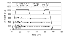
【解決手段】本発明は、基板10上にGaN電子走行層14を形成する工程と、GaN電子走行層14上にInAlN電子供給層18を形成する工程と、InAlN電子供給層18を形成した後、In含有ガスを供給しつつ、基板10を昇温させる工程と、昇温が終了した後、InAlN電子供給層18上にGaN層20を形成する工程と、を有する半導体装置の製造方法である。
【選択図】図2
Description
2.55α+3.11β+3.19γ+3.55(1−α−β−γ)=3.55x+3.11(1−x)
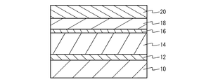
12 シード層
14 GaN電子走行層
16 スペーサ層
18 InAlN電子供給層
20 GaN層
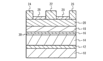
22 ゲート電極
24 ソース電極
26 ドレイン電極
28 保護膜
30 2次元電子ガス
Claims (10)
- 基板上に窒化物半導体からなる電子走行層を形成する工程と、
前記電子走行層上にInAlN層を形成する工程と、
前記InAlN層を形成した後、In含有ガスを供給しつつ、前記基板を昇温させる工程と、
前記昇温が終了した後、前記InAlN層上にGaN層を形成する工程と、を有することを特徴とする半導体装置の製造方法。 - 前記基板の温度の上昇に従い、前記In含有ガスの供給量を増やすことを特徴とする請求項1記載の半導体装置の製造方法。
- 前記In含有ガスとともに、Al含有ガスを供給しつつ、前記基板を昇温させることを特徴とする請求項1または2記載の半導体装置の製造方法。
- 前記基板の温度の上昇に従い、前記In含有ガスと前記Al含有ガスの供給量を増やすことを特徴とする請求項3記載の半導体装置の製造方法。
- 前記基板の昇温は、900℃以上であることを特徴とする請求項1から4のいずれか一項記載の半導体装置の製造方法。
- 前記InAlN層は、600℃から800℃の範囲で成長されることを特徴とする請求項1から5のいずれか一項記載の半導体装置の製造方法。
- 前記In含有ガスは、トリメチルインジウムであることを特徴とする請求項1から6のいずれか一項記載の半導体装置の製造方法。
- 前記Al含有ガスは、トリメチルアルミニウムまたはトリエチルアルミニウムであることを特徴とする請求項3または4記載の半導体装置の製造方法。
- 基板上にInAlN層を成長する工程と、
In含有ガスを供給しつつ、前記基板を900℃以上に昇温する工程と、
前記InAlN層上に半導体層を成長する工程と、を有することを特徴とする半導体装置の製造方法。 - 前記半導体層は、GaN層であることを特徴とする請求項9記載の半導体装置の製造方法。
Priority Applications (3)
| Application Number | Priority Date | Filing Date | Title |
|---|---|---|---|
| JP2011128649A JP5803303B2 (ja) | 2011-06-08 | 2011-06-08 | 半導体装置の製造方法 |
| US13/489,647 US20120315742A1 (en) | 2011-06-08 | 2012-06-06 | Method for forming nitride semiconductor device |
| US14/983,864 US20160111274A1 (en) | 2011-06-08 | 2015-12-30 | Method for forming nitride semiconductor device |
Applications Claiming Priority (1)
| Application Number | Priority Date | Filing Date | Title |
|---|---|---|---|
| JP2011128649A JP5803303B2 (ja) | 2011-06-08 | 2011-06-08 | 半導体装置の製造方法 |
Publications (2)
| Publication Number | Publication Date |
|---|---|
| JP2012256705A true JP2012256705A (ja) | 2012-12-27 |
| JP5803303B2 JP5803303B2 (ja) | 2015-11-04 |
Family
ID=47528026
Family Applications (1)
| Application Number | Title | Priority Date | Filing Date |
|---|---|---|---|
| JP2011128649A Expired - Fee Related JP5803303B2 (ja) | 2011-06-08 | 2011-06-08 | 半導体装置の製造方法 |
Country Status (1)
| Country | Link |
|---|---|
| JP (1) | JP5803303B2 (ja) |
Cited By (2)
| Publication number | Priority date | Publication date | Assignee | Title |
|---|---|---|---|---|
| JP2014239159A (ja) * | 2013-06-07 | 2014-12-18 | 住友電気工業株式会社 | 半導体装置およびその製造方法 |
| JP2016058539A (ja) * | 2014-09-09 | 2016-04-21 | 三菱電機株式会社 | 高電子移動度トランジスタの製造方法 |
Citations (9)
| Publication number | Priority date | Publication date | Assignee | Title |
|---|---|---|---|---|
| JPH08293643A (ja) * | 1995-04-24 | 1996-11-05 | Sharp Corp | 化合物半導体発光素子およびその製造方法 |
| JPH09186363A (ja) * | 1995-12-27 | 1997-07-15 | Toshiba Corp | 半導体発光素子及びその製造方法 |
| JPH11354846A (ja) * | 1996-01-19 | 1999-12-24 | Matsushita Electric Ind Co Ltd | 窒化ガリウム系化合物半導体発光素子及び窒化ガリウム系化合物半導体の製造方法 |
| JP2007165431A (ja) * | 2005-12-12 | 2007-06-28 | Nippon Telegr & Teleph Corp <Ntt> | 電界効果型トランジスタおよびその製造方法 |
| JP2009032713A (ja) * | 2007-07-24 | 2009-02-12 | National Institute Of Advanced Industrial & Technology | GaNをチャネル層とする窒化物半導体トランジスタ及びその作製方法 |
| JP2010182812A (ja) * | 2009-02-04 | 2010-08-19 | Fujitsu Ltd | 化合物半導体装置及びその製造方法 |
| JP2010199597A (ja) * | 2010-04-09 | 2010-09-09 | Fujitsu Ltd | 化合物半導体装置の製造方法 |
| WO2010100699A1 (ja) * | 2009-03-06 | 2010-09-10 | パナソニック株式会社 | 窒化物半導体の結晶成長方法および半導体装置の製造方法 |
| JP2011079728A (ja) * | 2009-09-14 | 2011-04-21 | Sumitomo Electric Ind Ltd | 窒化物半導体エピタキシャル層の形成方法および窒化物半導体デバイスの製造方法 |
-
2011
- 2011-06-08 JP JP2011128649A patent/JP5803303B2/ja not_active Expired - Fee Related
Patent Citations (9)
| Publication number | Priority date | Publication date | Assignee | Title |
|---|---|---|---|---|
| JPH08293643A (ja) * | 1995-04-24 | 1996-11-05 | Sharp Corp | 化合物半導体発光素子およびその製造方法 |
| JPH09186363A (ja) * | 1995-12-27 | 1997-07-15 | Toshiba Corp | 半導体発光素子及びその製造方法 |
| JPH11354846A (ja) * | 1996-01-19 | 1999-12-24 | Matsushita Electric Ind Co Ltd | 窒化ガリウム系化合物半導体発光素子及び窒化ガリウム系化合物半導体の製造方法 |
| JP2007165431A (ja) * | 2005-12-12 | 2007-06-28 | Nippon Telegr & Teleph Corp <Ntt> | 電界効果型トランジスタおよびその製造方法 |
| JP2009032713A (ja) * | 2007-07-24 | 2009-02-12 | National Institute Of Advanced Industrial & Technology | GaNをチャネル層とする窒化物半導体トランジスタ及びその作製方法 |
| JP2010182812A (ja) * | 2009-02-04 | 2010-08-19 | Fujitsu Ltd | 化合物半導体装置及びその製造方法 |
| WO2010100699A1 (ja) * | 2009-03-06 | 2010-09-10 | パナソニック株式会社 | 窒化物半導体の結晶成長方法および半導体装置の製造方法 |
| JP2011079728A (ja) * | 2009-09-14 | 2011-04-21 | Sumitomo Electric Ind Ltd | 窒化物半導体エピタキシャル層の形成方法および窒化物半導体デバイスの製造方法 |
| JP2010199597A (ja) * | 2010-04-09 | 2010-09-09 | Fujitsu Ltd | 化合物半導体装置の製造方法 |
Cited By (2)
| Publication number | Priority date | Publication date | Assignee | Title |
|---|---|---|---|---|
| JP2014239159A (ja) * | 2013-06-07 | 2014-12-18 | 住友電気工業株式会社 | 半導体装置およびその製造方法 |
| JP2016058539A (ja) * | 2014-09-09 | 2016-04-21 | 三菱電機株式会社 | 高電子移動度トランジスタの製造方法 |
Also Published As
| Publication number | Publication date |
|---|---|
| JP5803303B2 (ja) | 2015-11-04 |
Similar Documents
| Publication | Publication Date | Title |
|---|---|---|
| JP6318474B2 (ja) | 半導体装置の製造方法 | |
| JP5785103B2 (ja) | ヘテロ接合型電界効果トランジスタ用のエピタキシャルウエハ | |
| US20160111274A1 (en) | Method for forming nitride semiconductor device | |
| JP2013145782A (ja) | ヘテロ接合型電界効果トランジスタ用のエピタキシャルウエハ | |
| JP6729416B2 (ja) | 窒化物半導体デバイス及び窒化物半導体デバイスの製造方法 | |
| JP2012015304A (ja) | 半導体装置 | |
| JP2016207748A (ja) | 半導体装置の製造方法および半導体装置 | |
| JP2017168627A (ja) | 高電子移動度トランジスタ及び高電子移動度トランジスタの製造方法 | |
| JP5914999B2 (ja) | 半導体装置の製造方法 | |
| JP2018056591A (ja) | 窒化物半導体装置および窒化物半導体基板 | |
| JP4468744B2 (ja) | 窒化物半導体薄膜の作製方法 | |
| JP5817283B2 (ja) | 半導体装置の製造方法 | |
| CN104091759B (zh) | 一种蓝宝石衬底AlN外延层高电子迁移率晶体管生长方法 | |
| CN113921608B (zh) | Iii族氮化物层叠物、半导体元件和iii族氮化物层叠物的制造方法 | |
| JP6305137B2 (ja) | 窒化物半導体積層物および半導体装置 | |
| CN102820211A (zh) | 制备非极性A面GaN薄膜的方法 | |
| JP5776344B2 (ja) | 半導体装置 | |
| JP5803303B2 (ja) | 半導体装置の製造方法 | |
| JP2014241387A (ja) | 基板、基板の製造方法、及び電子装置 | |
| JP2014090065A (ja) | 窒化物系半導体エピタキシャルウエハ及び窒化物系電界効果型トランジスタ | |
| JP6848584B2 (ja) | 窒化物半導体層の成長方法 | |
| CN105405761A (zh) | 高电子迁移率晶体管的制造方法 | |
| JP2013187461A (ja) | 半導体素子およびその製造方法 | |
| CN101901760B (zh) | 基于c面SiC衬底上极性c面GaN的MOCVD生长方法 | |
| JP5455875B2 (ja) | エピタキシャル基板の製造方法 |
Legal Events
| Date | Code | Title | Description |
|---|---|---|---|
| A621 | Written request for application examination |
Free format text: JAPANESE INTERMEDIATE CODE: A621 Effective date: 20140522 |
|
| A131 | Notification of reasons for refusal |
Free format text: JAPANESE INTERMEDIATE CODE: A131 Effective date: 20150210 |
|
| A977 | Report on retrieval |
Free format text: JAPANESE INTERMEDIATE CODE: A971007 Effective date: 20150212 |
|
| A521 | Written amendment |
Free format text: JAPANESE INTERMEDIATE CODE: A523 Effective date: 20150413 |
|
| TRDD | Decision of grant or rejection written | ||
| A01 | Written decision to grant a patent or to grant a registration (utility model) |
Free format text: JAPANESE INTERMEDIATE CODE: A01 Effective date: 20150804 |
|
| A61 | First payment of annual fees (during grant procedure) |
Free format text: JAPANESE INTERMEDIATE CODE: A61 Effective date: 20150817 |
|
| R150 | Certificate of patent or registration of utility model |
Ref document number: 5803303 Country of ref document: JP Free format text: JAPANESE INTERMEDIATE CODE: R150 |
|
| R250 | Receipt of annual fees |
Free format text: JAPANESE INTERMEDIATE CODE: R250 |
|
| LAPS | Cancellation because of no payment of annual fees |