JP2012507155A - オプトエレクトロニクス半導体チップおよびオプトエレクトロニクス半導体チップの製造方法 - Google Patents
オプトエレクトロニクス半導体チップおよびオプトエレクトロニクス半導体チップの製造方法 Download PDFInfo
- Publication number
- JP2012507155A JP2012507155A JP2011533530A JP2011533530A JP2012507155A JP 2012507155 A JP2012507155 A JP 2012507155A JP 2011533530 A JP2011533530 A JP 2011533530A JP 2011533530 A JP2011533530 A JP 2011533530A JP 2012507155 A JP2012507155 A JP 2012507155A
- Authority
- JP
- Japan
- Prior art keywords
- layer
- lattice
- semiconductor chip
- lattice layer
- active
- Prior art date
- Legal status (The legal status is an assumption and is not a legal conclusion. Google has not performed a legal analysis and makes no representation as to the accuracy of the status listed.)
- Granted
Links
Images


Classifications
-
- H—ELECTRICITY
- H01—ELECTRIC ELEMENTS
- H01S—DEVICES USING THE PROCESS OF LIGHT AMPLIFICATION BY STIMULATED EMISSION OF RADIATION [LASER] TO AMPLIFY OR GENERATE LIGHT; DEVICES USING STIMULATED EMISSION OF ELECTROMAGNETIC RADIATION IN WAVE RANGES OTHER THAN OPTICAL
- H01S5/00—Semiconductor lasers
- H01S5/10—Construction or shape of the optical resonator, e.g. extended or external cavity, coupled cavities, bent-guide, varying width, thickness or composition of the active region
- H01S5/12—Construction or shape of the optical resonator, e.g. extended or external cavity, coupled cavities, bent-guide, varying width, thickness or composition of the active region the resonator having a periodic structure, e.g. in distributed feedback [DFB] lasers
-
- H—ELECTRICITY
- H01—ELECTRIC ELEMENTS
- H01S—DEVICES USING THE PROCESS OF LIGHT AMPLIFICATION BY STIMULATED EMISSION OF RADIATION [LASER] TO AMPLIFY OR GENERATE LIGHT; DEVICES USING STIMULATED EMISSION OF ELECTROMAGNETIC RADIATION IN WAVE RANGES OTHER THAN OPTICAL
- H01S5/00—Semiconductor lasers
- H01S5/04—Processes or apparatus for excitation, e.g. pumping, e.g. by electron beams
- H01S5/042—Electrical excitation ; Circuits therefor
- H01S5/0421—Electrical excitation ; Circuits therefor characterised by the semiconducting contacting layers
-
- H—ELECTRICITY
- H01—ELECTRIC ELEMENTS
- H01S—DEVICES USING THE PROCESS OF LIGHT AMPLIFICATION BY STIMULATED EMISSION OF RADIATION [LASER] TO AMPLIFY OR GENERATE LIGHT; DEVICES USING STIMULATED EMISSION OF ELECTROMAGNETIC RADIATION IN WAVE RANGES OTHER THAN OPTICAL
- H01S5/00—Semiconductor lasers
- H01S5/06—Arrangements for controlling the laser output parameters, e.g. by operating on the active medium
- H01S5/062—Arrangements for controlling the laser output parameters, e.g. by operating on the active medium by varying the potential of the electrodes
- H01S5/0625—Arrangements for controlling the laser output parameters, e.g. by operating on the active medium by varying the potential of the electrodes in multi-section lasers
- H01S5/06255—Controlling the frequency of the radiation
- H01S5/06256—Controlling the frequency of the radiation with DBR-structure
-
- H—ELECTRICITY
- H01—ELECTRIC ELEMENTS
- H01S—DEVICES USING THE PROCESS OF LIGHT AMPLIFICATION BY STIMULATED EMISSION OF RADIATION [LASER] TO AMPLIFY OR GENERATE LIGHT; DEVICES USING STIMULATED EMISSION OF ELECTROMAGNETIC RADIATION IN WAVE RANGES OTHER THAN OPTICAL
- H01S5/00—Semiconductor lasers
- H01S5/10—Construction or shape of the optical resonator, e.g. extended or external cavity, coupled cavities, bent-guide, varying width, thickness or composition of the active region
- H01S5/12—Construction or shape of the optical resonator, e.g. extended or external cavity, coupled cavities, bent-guide, varying width, thickness or composition of the active region the resonator having a periodic structure, e.g. in distributed feedback [DFB] lasers
- H01S5/1228—DFB lasers with a complex coupled grating, e.g. gain or loss coupling
-
- H—ELECTRICITY
- H01—ELECTRIC ELEMENTS
- H01S—DEVICES USING THE PROCESS OF LIGHT AMPLIFICATION BY STIMULATED EMISSION OF RADIATION [LASER] TO AMPLIFY OR GENERATE LIGHT; DEVICES USING STIMULATED EMISSION OF ELECTROMAGNETIC RADIATION IN WAVE RANGES OTHER THAN OPTICAL
- H01S5/00—Semiconductor lasers
- H01S5/10—Construction or shape of the optical resonator, e.g. extended or external cavity, coupled cavities, bent-guide, varying width, thickness or composition of the active region
- H01S5/12—Construction or shape of the optical resonator, e.g. extended or external cavity, coupled cavities, bent-guide, varying width, thickness or composition of the active region the resonator having a periodic structure, e.g. in distributed feedback [DFB] lasers
- H01S5/1231—Grating growth or overgrowth details
-
- H—ELECTRICITY
- H01—ELECTRIC ELEMENTS
- H01S—DEVICES USING THE PROCESS OF LIGHT AMPLIFICATION BY STIMULATED EMISSION OF RADIATION [LASER] TO AMPLIFY OR GENERATE LIGHT; DEVICES USING STIMULATED EMISSION OF ELECTROMAGNETIC RADIATION IN WAVE RANGES OTHER THAN OPTICAL
- H01S5/00—Semiconductor lasers
- H01S5/20—Structure or shape of the semiconductor body to guide the optical wave ; Confining structures perpendicular to the optical axis, e.g. index or gain guiding, stripe geometry, broad area lasers, gain tailoring, transverse or lateral reflectors, special cladding structures, MQW barrier reflection layers
- H01S5/2054—Methods of obtaining the confinement
- H01S5/2081—Methods of obtaining the confinement using special etching techniques
- H01S5/209—Methods of obtaining the confinement using special etching techniques special etch stop layers
-
- H—ELECTRICITY
- H10—SEMICONDUCTOR DEVICES; ELECTRIC SOLID-STATE DEVICES NOT OTHERWISE PROVIDED FOR
- H10H—INORGANIC LIGHT-EMITTING SEMICONDUCTOR DEVICES HAVING POTENTIAL BARRIERS
- H10H20/00—Individual inorganic light-emitting semiconductor devices having potential barriers, e.g. light-emitting diodes [LED]
- H10H20/80—Constructional details
- H10H20/81—Bodies
- H10H20/816—Bodies having carrier transport control structures, e.g. highly-doped semiconductor layers or current-blocking structures
Landscapes
- Physics & Mathematics (AREA)
- Condensed Matter Physics & Semiconductors (AREA)
- General Physics & Mathematics (AREA)
- Electromagnetism (AREA)
- Optics & Photonics (AREA)
- Semiconductor Lasers (AREA)
Abstract
Description
活性層は、動作時に放射方向に沿って電磁放射を放出することに適している活性領域を有し、
第1の格子層は、放射方向に対して垂直に延在し、格子線として構成されている複数のストライプを有し、それらのストライプ間には中間空間が配置されており、
第2の格子層は、第1の格子層のストライプおよび中間空間を覆い、かつ、非エピタキシャル被着方法によって被着されている透明材料を有する。
A)動作時に放射方向に沿って電磁放射を放出することに適している活性領域を備えた活性層を準備するステップと、
B)放射方向に対して垂直に延在し、かつ、格子線として構成されている複数のストライプとそれらストライプ間に配置されている中間空間とを放射方向に沿って有する第1の格子層を活性層上に被着するステップと、
C)非エピタキシャル被着方法によって被着される透明材料を有する第2の格子層を第1の格子層上に被着し、第1の格子層のストライプおよび中間空間を覆うステップとを有する。
B1)第1の格子層を大面積で被着するステップ、
B2)活性領域の放射方向に対して垂直に延びる複数のストライプと、それらのストライプ間に位置する中間空間とを備えたマスク層を被着するステップ、
B3)マスク層の中間空間の領域において第1の格子層を湿式化学的にエッチングするステップ。
Claims (15)
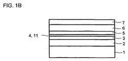
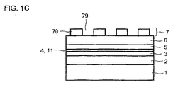
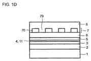
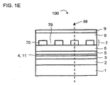
- 相互に重なって配置されている複数の層を備えた半導体積層体を有するオプトエレクトロニクス半導体チップにおいて、
活性層(4)と、該活性層(4)上の第1の格子層(7)と、該第1の格子層(7)上の第2の格子層(8)とを有し、
前記活性層(4)は、動作時に放射方向(99)に沿って電磁放射を放出することに適している活性領域(11)を有し、
前記第1の格子層(7)は、前記放射方向(99)に対して垂直に延在し、格子線として構成されている複数のストライプ(70)を有し、該ストライプ(70)間には中間空間(79)が配置されており、
前記第2の格子層(8)は、前記第1の格子層(7)の前記ストライプ(70)および前記中間空間(79)を覆い、かつ、非エピタキシャル被着方法によって被着されている透明材料を有する、
ことを特徴とする、オプトエレクトロニクス半導体チップ。 - 前記第2の格子層(8)は前記第1の格子層(7)よりも低い屈折率を有する、請求項1記載の半導体チップ。
- 前記第2の格子層(8)の屈折率は2.5以下であり、例えば2以下である、請求項1または2記載の半導体チップ。
- 前記第2の格子層(8)の前記透明材料は、透明導電性酸化物、例えば酸化亜鉛および/または酸化インジウムスズを含む、請求項1から3までのいずれか1項記載の半導体チップ。
- 前記第2の格子層(8)は蒸着またはスパッタリングを用いて被着されている、請求項1から4までのいずれか1項記載の半導体チップ。
- 前記第1の格子層(7)はコンタクト層として構成されている、請求項1から5までのいずれか1項記載の半導体チップ。
- 前記第1の格子層(7)と前記活性層(4)との間には構造化されていないコンタクト層(10)が設けられている、請求項1から6までのいずれか1項記載の半導体チップ。
- 前記第1の格子層(7)と前記構造化されていないコンタクト層(10)との間には中間層(71)が配置されている、請求項7記載の半導体チップ。
- 前記中間層(71)はエッチストップ層として構成されている、請求項8記載の半導体チップ。
- 前記第1の格子層(7)および前記第2の格子層(8)は、前記半導体積層体の配置方向に沿って、前記活性領域(11)の上方に配置されている、請求項1から9までのいずれか1項記載の半導体チップ。
- 前記第1の格子層(7)および前記第2の格子層(8)は、縦方向において、前記活性領域(11)からずらされて配置されている、請求項1から9までのいずれか1項記載の半導体チップ。
- 前記第2の格子層(8)上に電極(9)が配置されている、請求項1から11までのいずれか1項記載の半導体チップ。
- 相互に重なって配置されている複数の層を備えた半導体積層体を有するオプトエレクトロニクス半導体チップの製造方法において、
A)動作時に放射方向(99)に沿って電磁放射を放出することに適している活性領域(11)を備えた活性層(4)を準備するステップと、
B)前記放射方向(99)に対して垂直に延在し、かつ、格子線として構成されている複数のストライプ(70)と、該ストライプ(70)間に配置されている中間空間(79)とを前記放射方向(99)に沿って有する第1の格子層(7)を前記活性層(4)上に被着するステップと、
C)非エピタキシャル被着方法によって被着される透明材料を有する第2の格子層(8)を前記第1の格子層(7)上に被着し、前記第1の格子層(7)の前記ストライプ(70)および前記中間空間(79)を覆うステップとを有することを特徴とする、オプトエレクトロニクス半導体チップの製造方法。 - 前記透明材料は透明導電性酸化物を含み、前記透明材料を前記ステップCにおいて蒸着またはスパッタリングによって被着させる、請求項13記載の方法。
- 前記ステップAまたは前記ステップBは別の部分ステップ、すなわち、
B1)前記第1の格子層(7)を大面積で被着するステップ、
を有し、かつ、
前記ステップBは別の部分ステップ、すなわち
B2)前記活性領域(11)の前記放射方向(99)に対して垂直に延在する複数のストライプと、該ストライプ間に存在する中間空間とを備えたマスク層を被着するステップ、
B3)前記マスク層の中間空間の領域内に前記第1の格子層(7)を湿式化学的にエッチングするステップ、
を有する、請求項13または14記載の方法。
Applications Claiming Priority (3)
| Application Number | Priority Date | Filing Date | Title |
|---|---|---|---|
| DE102008054217.2 | 2008-10-31 | ||
| DE102008054217A DE102008054217A1 (de) | 2008-10-31 | 2008-10-31 | Optoelektronischer Halbleiterchip und Verfahren zur Herstellung eines optoelektronischen Halbleiterchips |
| PCT/DE2009/001416 WO2010048918A1 (de) | 2008-10-31 | 2009-10-12 | Optoelektronischer halbleiterchip und verfahren zur herstellung eines optoelektronischen halbleiterchips |
Publications (3)
| Publication Number | Publication Date |
|---|---|
| JP2012507155A true JP2012507155A (ja) | 2012-03-22 |
| JP2012507155A5 JP2012507155A5 (ja) | 2012-11-22 |
| JP5717640B2 JP5717640B2 (ja) | 2015-05-13 |
Family
ID=41615393
Family Applications (1)
| Application Number | Title | Priority Date | Filing Date |
|---|---|---|---|
| JP2011533530A Expired - Fee Related JP5717640B2 (ja) | 2008-10-31 | 2009-10-12 | オプトエレクトロニクス半導体チップおよびオプトエレクトロニクス半導体チップの製造方法 |
Country Status (4)
| Country | Link |
|---|---|
| US (1) | US8536603B2 (ja) |
| JP (1) | JP5717640B2 (ja) |
| DE (1) | DE102008054217A1 (ja) |
| WO (1) | WO2010048918A1 (ja) |
Families Citing this family (5)
| Publication number | Priority date | Publication date | Assignee | Title |
|---|---|---|---|---|
| JP6454132B2 (ja) * | 2014-11-06 | 2019-01-16 | 株式会社ミツバ | ワイパシステム |
| JP7159844B2 (ja) * | 2018-12-17 | 2022-10-25 | 日本電信電話株式会社 | 半導体レーザ |
| US10916915B2 (en) * | 2018-12-21 | 2021-02-09 | National Sun Yat-Sen University | Distributed feedback semiconductor laser device |
| US11133649B2 (en) * | 2019-06-21 | 2021-09-28 | Palo Alto Research Center Incorporated | Index and gain coupled distributed feedback laser |
| DE102024126995A1 (de) * | 2024-09-19 | 2026-03-19 | Ams-Osram International Gmbh | Kantenemittierender halbleiterlaser und verfahren zur herstellung eines kantenemittierenden halbleiterlasers |
Citations (8)
| Publication number | Priority date | Publication date | Assignee | Title |
|---|---|---|---|---|
| JPH01175277A (ja) * | 1987-12-29 | 1989-07-11 | Fujitsu Ltd | 半導体発光装置及び光変調方法 |
| JPH06342960A (ja) * | 1993-04-07 | 1994-12-13 | Sony Corp | 選択エッチング方法ならびに光電子素子およびその製造方法 |
| JPH0974249A (ja) * | 1995-09-06 | 1997-03-18 | Toshiba Corp | 半導体発光装置 |
| JPH11220212A (ja) * | 1998-02-02 | 1999-08-10 | Toshiba Corp | 光素子、光素子の駆動方法及び半導体レーザ素子 |
| JP2001223384A (ja) * | 2000-02-08 | 2001-08-17 | Toshiba Corp | 半導体発光素子 |
| US20040165637A1 (en) * | 2002-03-22 | 2004-08-26 | Bullington Jeff A. | Laser-to-fiber coupling |
| JP2007234824A (ja) * | 2006-02-28 | 2007-09-13 | Canon Inc | 垂直共振器型面発光レーザ |
| JP2007536718A (ja) * | 2004-05-03 | 2007-12-13 | メルク パテント ゲーエムベーハー | 有機半導体を含む電子デバイス |
Family Cites Families (49)
| Publication number | Priority date | Publication date | Assignee | Title |
|---|---|---|---|---|
| JPS62163385A (ja) * | 1986-01-14 | 1987-07-20 | Sony Corp | 分布帰還型半導体レ−ザの製造方法 |
| US5177758A (en) * | 1989-06-14 | 1993-01-05 | Hitachi, Ltd. | Semiconductor laser device with plural active layers and changing optical properties |
| US5070509A (en) * | 1990-08-09 | 1991-12-03 | Eastman Kodak Company | Surface emitting, low threshold (SELTH) laser diode |
| JP2982422B2 (ja) * | 1991-09-20 | 1999-11-22 | 三菱電機株式会社 | 半導体レーザおよびその製造方法 |
| US5206877A (en) * | 1992-02-18 | 1993-04-27 | Eastman Kodak Company | Distributed feedback laser diodes with selectively placed lossy sections |
| JPH08255954A (ja) * | 1995-03-17 | 1996-10-01 | Mitsubishi Electric Corp | 半導体レーザの構造及びその製造方法 |
| JP4017196B2 (ja) * | 1995-03-22 | 2007-12-05 | シャープ株式会社 | 分布帰還型半導体レーザ装置 |
| TW304310B (ja) * | 1995-05-31 | 1997-05-01 | Siemens Ag | |
| US5617436A (en) | 1995-06-07 | 1997-04-01 | Cornell Research Foundation, Inc. | Strain-compensated multiple quantum well laser structures |
| US6104739A (en) * | 1997-12-24 | 2000-08-15 | Nortel Networks Corporation | Series of strongly complex coupled DFB lasers |
| JPH11274637A (ja) * | 1998-03-20 | 1999-10-08 | Pioneer Electron Corp | 横結合分布帰還リッジ型半導体レーザ及びその製造方法 |
| JP3763667B2 (ja) * | 1998-04-23 | 2006-04-05 | 株式会社東芝 | 半導体発光素子 |
| JP2000277869A (ja) * | 1999-03-29 | 2000-10-06 | Mitsubishi Electric Corp | 変調器集積型半導体レーザ装置及びその製造方法 |
| US6365428B1 (en) * | 2000-06-15 | 2002-04-02 | Sandia Corporation | Embedded high-contrast distributed grating structures |
| US20020064203A1 (en) * | 2000-09-14 | 2002-05-30 | Bardia Pezeshki | Strip-loaded tunable distributed feedback laser |
| US6947463B2 (en) * | 2000-10-23 | 2005-09-20 | The Furukawa Electric Co., Ltd. | Semiconductor laser device for use in a laser module |
| JP2002305350A (ja) * | 2001-01-31 | 2002-10-18 | Furukawa Electric Co Ltd:The | 分布帰還型半導体レーザ素子及びその作製方法 |
| US6891870B2 (en) * | 2001-11-09 | 2005-05-10 | Corning Lasertron, Inc. | Distributed feedback laser for isolator-free operation |
| KR100453814B1 (ko) * | 2002-02-07 | 2004-10-20 | 한국전자통신연구원 | 이종 회절격자를 가지는 반도체 광소자 및 그 제조 방법 |
| US7035305B2 (en) * | 2002-05-10 | 2006-04-25 | Bookham Technology, Plc | Monolithically integrated high power laser optical device |
| US6608855B1 (en) * | 2002-05-31 | 2003-08-19 | Applied Optoelectronics, Inc. | Single-mode DBR laser with improved phase-shift section |
| US6638773B1 (en) * | 2002-05-31 | 2003-10-28 | Applied Optoelectronics, Inc. | Method for fabricating single-mode DBR laser with improved yield |
| US7065123B2 (en) * | 2002-06-27 | 2006-06-20 | Anritsu Corporation | Distributed feedback semiconductor laser for outputting beam of single wavelength |
| US6649439B1 (en) * | 2002-08-01 | 2003-11-18 | Northrop Grumman Corporation | Semiconductor-air gap grating fabrication using a sacrificial layer process |
| US6771682B2 (en) * | 2002-08-12 | 2004-08-03 | Infinera Corporation | Electrical isolation of optical components in photonic integrated circuits (PICs) |
| US7041529B2 (en) * | 2002-10-23 | 2006-05-09 | Shin-Etsu Handotai Co., Ltd. | Light-emitting device and method of fabricating the same |
| US7095058B2 (en) * | 2003-03-21 | 2006-08-22 | Intel Corporation | System and method for an improved light-emitting device |
| JP2005063838A (ja) * | 2003-08-13 | 2005-03-10 | Toshiba Matsushita Display Technology Co Ltd | 光学デバイス及び有機el表示装置 |
| TWI230474B (en) * | 2004-04-13 | 2005-04-01 | United Epitaxy Co Ltd | High luminance indium gallium aluminum nitride light emitting, device and manufacture method thereof |
| JP4511440B2 (ja) * | 2004-10-05 | 2010-07-28 | 三星モバイルディスプレイ株式會社 | 有機発光素子及び有機発光素子の製造方法 |
| US8605769B2 (en) * | 2004-12-08 | 2013-12-10 | Sumitomo Electric Industries, Ltd. | Semiconductor laser device and manufacturing method thereof |
| JP4253302B2 (ja) * | 2005-01-06 | 2009-04-08 | 株式会社東芝 | 有機エレクトロルミネッセンス素子およびその製造方法 |
| US7860141B2 (en) * | 2005-04-28 | 2010-12-28 | Kyoto University | Photonic crystal laser |
| US7583719B2 (en) * | 2005-08-24 | 2009-09-01 | Applied Optoelectronics, Inc, | Complex-coupled distributed feedback semiconductor laser |
| US8121170B2 (en) * | 2005-08-24 | 2012-02-21 | Applied Optoelectronics, Inc. | Gain-coupled distributed feedback semiconductor laser including first-order and second-order gratings |
| US7627012B2 (en) * | 2005-08-24 | 2009-12-01 | Applied Optoelectronics, Inc. | Distributed feedback semiconductor laser including wavelength monitoring section |
| US7349456B2 (en) * | 2005-10-07 | 2008-03-25 | Agilent Technologies, Inc. | Gain-coupled distributed quantum cascade laser |
| JP4857702B2 (ja) * | 2005-10-13 | 2012-01-18 | 三菱電機株式会社 | 集積型光半導体装置の製造方法 |
| DE102006024220A1 (de) | 2006-04-13 | 2007-10-18 | Osram Opto Semiconductors Gmbh | Optoelektronisches Halbleiterbauelement |
| JP4951267B2 (ja) * | 2006-04-27 | 2012-06-13 | 日本オプネクスト株式会社 | 半導体レーザ素子の製造方法 |
| JP2007299791A (ja) * | 2006-04-27 | 2007-11-15 | Sumitomo Electric Ind Ltd | 半導体光素子 |
| JP2008098387A (ja) * | 2006-10-12 | 2008-04-24 | Sumitomo Electric Ind Ltd | 回折格子の作製方法 |
| CN101222009A (zh) * | 2007-01-12 | 2008-07-16 | 清华大学 | 发光二极管 |
| KR100839343B1 (ko) * | 2007-01-23 | 2008-06-17 | 광주과학기술원 | 반도체 레이저 소자 및 그 제조 방법 |
| US7680371B2 (en) * | 2007-02-13 | 2010-03-16 | National Research Council Of Canada | Interface device for performing mode transformation in optical waveguides |
| JP2009049044A (ja) * | 2007-08-13 | 2009-03-05 | Sumitomo Electric Ind Ltd | 半導体レーザを作製する方法 |
| DE102007044848B4 (de) * | 2007-09-13 | 2009-12-31 | Fraunhofer-Gesellschaft zur Förderung der angewandten Forschung e.V. | Halbleiterlaser und Verfahren zum Betreiben eines Halbleiterlasers |
| JP5026905B2 (ja) * | 2007-10-02 | 2012-09-19 | 富士通株式会社 | 半導体発光素子及びその製造方法 |
| JP5359154B2 (ja) * | 2008-09-26 | 2013-12-04 | 住友電気工業株式会社 | 回折格子の形成方法および分布帰還型半導体レーザの製造方法 |
-
2008
- 2008-10-31 DE DE102008054217A patent/DE102008054217A1/de active Granted
-
2009
- 2009-10-12 WO PCT/DE2009/001416 patent/WO2010048918A1/de not_active Ceased
- 2009-10-12 US US13/123,779 patent/US8536603B2/en active Active
- 2009-10-12 JP JP2011533530A patent/JP5717640B2/ja not_active Expired - Fee Related
Patent Citations (8)
| Publication number | Priority date | Publication date | Assignee | Title |
|---|---|---|---|---|
| JPH01175277A (ja) * | 1987-12-29 | 1989-07-11 | Fujitsu Ltd | 半導体発光装置及び光変調方法 |
| JPH06342960A (ja) * | 1993-04-07 | 1994-12-13 | Sony Corp | 選択エッチング方法ならびに光電子素子およびその製造方法 |
| JPH0974249A (ja) * | 1995-09-06 | 1997-03-18 | Toshiba Corp | 半導体発光装置 |
| JPH11220212A (ja) * | 1998-02-02 | 1999-08-10 | Toshiba Corp | 光素子、光素子の駆動方法及び半導体レーザ素子 |
| JP2001223384A (ja) * | 2000-02-08 | 2001-08-17 | Toshiba Corp | 半導体発光素子 |
| US20040165637A1 (en) * | 2002-03-22 | 2004-08-26 | Bullington Jeff A. | Laser-to-fiber coupling |
| JP2007536718A (ja) * | 2004-05-03 | 2007-12-13 | メルク パテント ゲーエムベーハー | 有機半導体を含む電子デバイス |
| JP2007234824A (ja) * | 2006-02-28 | 2007-09-13 | Canon Inc | 垂直共振器型面発光レーザ |
Also Published As
| Publication number | Publication date |
|---|---|
| JP5717640B2 (ja) | 2015-05-13 |
| DE102008054217A1 (de) | 2010-05-06 |
| US20110235664A1 (en) | 2011-09-29 |
| WO2010048918A1 (de) | 2010-05-06 |
| US8536603B2 (en) | 2013-09-17 |
Similar Documents
| Publication | Publication Date | Title |
|---|---|---|
| US12062887B2 (en) | Semiconductor laser diode | |
| US6855570B2 (en) | Compound semiconductor laser | |
| US6990132B2 (en) | Laser diode with metal-oxide upper cladding layer | |
| JP5963004B2 (ja) | 窒化物半導体発光素子 | |
| US8558245B2 (en) | Optical semiconductor device having ridge structure formed on active layer containing p-type region and its manufacture method | |
| JP5717640B2 (ja) | オプトエレクトロニクス半導体チップおよびオプトエレクトロニクス半導体チップの製造方法 | |
| JP2019009196A (ja) | 半導体レーザ | |
| KR20110093839A (ko) | 수직 방출 방향을 갖는 표면 방출 반도체 레이저 소자 | |
| JP7604595B2 (ja) | 半導体レーザダイオードおよび半導体レーザダイオードの製造方法 | |
| JP4045639B2 (ja) | 半導体レーザおよび半導体発光素子 | |
| US20250062594A1 (en) | Semiconductor laser and method for producing a semiconductor laser | |
| US20240396306A1 (en) | Nitride semiconductor light-emitting element | |
| JP2003142773A (ja) | 半導体発光装置 | |
| KR100584333B1 (ko) | 반도체 레이저 장치 및 그 제조방법 | |
| JP3950473B2 (ja) | 化合物半導体レーザ | |
| KR100978570B1 (ko) | 발광소자 | |
| JP5304428B2 (ja) | 半導体レーザ | |
| JP2022081994A (ja) | 半導体レーザ素子、およびエピタキシャル基板 | |
| CN115021081A (zh) | 发光芯片和激光器 | |
| JP2007043215A (ja) | 化合物半導体レーザ | |
| JP2007149937A (ja) | 光半導体素子 | |
| JPWO2016157739A1 (ja) | 半導体発光素子 | |
| JP2009266854A (ja) | 半導体レーザチップ及び半導体レーザ素子 |
Legal Events
| Date | Code | Title | Description |
|---|---|---|---|
| A521 | Request for written amendment filed |
Free format text: JAPANESE INTERMEDIATE CODE: A523 Effective date: 20121004 |
|
| A621 | Written request for application examination |
Free format text: JAPANESE INTERMEDIATE CODE: A621 Effective date: 20121004 |
|
| A977 | Report on retrieval |
Free format text: JAPANESE INTERMEDIATE CODE: A971007 Effective date: 20130830 |
|
| A131 | Notification of reasons for refusal |
Free format text: JAPANESE INTERMEDIATE CODE: A131 Effective date: 20130909 |
|
| A521 | Request for written amendment filed |
Free format text: JAPANESE INTERMEDIATE CODE: A523 Effective date: 20140307 |
|
| A131 | Notification of reasons for refusal |
Free format text: JAPANESE INTERMEDIATE CODE: A131 Effective date: 20140804 |
|
| A601 | Written request for extension of time |
Free format text: JAPANESE INTERMEDIATE CODE: A601 Effective date: 20141024 |
|
| A602 | Written permission of extension of time |
Free format text: JAPANESE INTERMEDIATE CODE: A602 Effective date: 20141031 |
|
| TRDD | Decision of grant or rejection written | ||
| A01 | Written decision to grant a patent or to grant a registration (utility model) |
Free format text: JAPANESE INTERMEDIATE CODE: A01 Effective date: 20150216 |
|
| A61 | First payment of annual fees (during grant procedure) |
Free format text: JAPANESE INTERMEDIATE CODE: A61 Effective date: 20150317 |
|
| R150 | Certificate of patent or registration of utility model |
Ref document number: 5717640 Country of ref document: JP Free format text: JAPANESE INTERMEDIATE CODE: R150 |
|
| R250 | Receipt of annual fees |
Free format text: JAPANESE INTERMEDIATE CODE: R250 |
|
| R250 | Receipt of annual fees |
Free format text: JAPANESE INTERMEDIATE CODE: R250 |
|
| R250 | Receipt of annual fees |
Free format text: JAPANESE INTERMEDIATE CODE: R250 |
|
| R250 | Receipt of annual fees |
Free format text: JAPANESE INTERMEDIATE CODE: R250 |
|
| R250 | Receipt of annual fees |
Free format text: JAPANESE INTERMEDIATE CODE: R250 |
|
| R250 | Receipt of annual fees |
Free format text: JAPANESE INTERMEDIATE CODE: R250 |
|
| R250 | Receipt of annual fees |
Free format text: JAPANESE INTERMEDIATE CODE: R250 |
|
| LAPS | Cancellation because of no payment of annual fees |