JP2012508404A - Light Emitting Diode Light Array on Mesh Platform - Google Patents
Light Emitting Diode Light Array on Mesh Platform Download PDFInfo
- Publication number
- JP2012508404A JP2012508404A JP2011543781A JP2011543781A JP2012508404A JP 2012508404 A JP2012508404 A JP 2012508404A JP 2011543781 A JP2011543781 A JP 2011543781A JP 2011543781 A JP2011543781 A JP 2011543781A JP 2012508404 A JP2012508404 A JP 2012508404A
- Authority
- JP
- Japan
- Prior art keywords
- display
- layer
- led
- display device
- led module
- Prior art date
- Legal status (The legal status is an assumption and is not a legal conclusion. Google has not performed a legal analysis and makes no representation as to the accuracy of the status listed.)
- Granted
Links
Images





Classifications
-
- G—PHYSICS
- G06—COMPUTING OR CALCULATING; COUNTING
- G06F—ELECTRIC DIGITAL DATA PROCESSING
- G06F3/00—Input arrangements for transferring data to be processed into a form capable of being handled by the computer; Output arrangements for transferring data from processing unit to output unit, e.g. interface arrangements
- G06F3/14—Digital output to display device ; Cooperation and interconnection of the display device with other functional units
- G06F3/1423—Digital output to display device ; Cooperation and interconnection of the display device with other functional units controlling a plurality of local displays, e.g. CRT and flat panel display
- G06F3/1446—Digital output to display device ; Cooperation and interconnection of the display device with other functional units controlling a plurality of local displays, e.g. CRT and flat panel display display composed of modules, e.g. video walls
-
- G—PHYSICS
- G09—EDUCATION; CRYPTOGRAPHY; DISPLAY; ADVERTISING; SEALS
- G09F—DISPLAYING; ADVERTISING; SIGNS; LABELS OR NAME-PLATES; SEALS
- G09F9/00—Indicating arrangements for variable information in which the information is built-up on a support by selection or combination of individual elements
- G09F9/30—Indicating arrangements for variable information in which the information is built-up on a support by selection or combination of individual elements in which the desired character or characters are formed by combining individual elements
- G09F9/33—Indicating arrangements for variable information in which the information is built-up on a support by selection or combination of individual elements in which the desired character or characters are formed by combining individual elements being semiconductor devices, e.g. diodes
-
- G—PHYSICS
- G09—EDUCATION; CRYPTOGRAPHY; DISPLAY; ADVERTISING; SEALS
- G09G—ARRANGEMENTS OR CIRCUITS FOR CONTROL OF INDICATING DEVICES USING STATIC MEANS TO PRESENT VARIABLE INFORMATION
- G09G3/00—Control arrangements or circuits, of interest only in connection with visual indicators other than cathode-ray tubes
- G09G3/20—Control arrangements or circuits, of interest only in connection with visual indicators other than cathode-ray tubes for presentation of an assembly of a number of characters, e.g. a page, by composing the assembly by combination of individual elements arranged in a matrix no fixed position being assigned to or needed to be assigned to the individual characters or partial characters
- G09G3/22—Control arrangements or circuits, of interest only in connection with visual indicators other than cathode-ray tubes for presentation of an assembly of a number of characters, e.g. a page, by composing the assembly by combination of individual elements arranged in a matrix no fixed position being assigned to or needed to be assigned to the individual characters or partial characters using controlled light sources
- G09G3/30—Control arrangements or circuits, of interest only in connection with visual indicators other than cathode-ray tubes for presentation of an assembly of a number of characters, e.g. a page, by composing the assembly by combination of individual elements arranged in a matrix no fixed position being assigned to or needed to be assigned to the individual characters or partial characters using controlled light sources using electroluminescent panels
- G09G3/32—Control arrangements or circuits, of interest only in connection with visual indicators other than cathode-ray tubes for presentation of an assembly of a number of characters, e.g. a page, by composing the assembly by combination of individual elements arranged in a matrix no fixed position being assigned to or needed to be assigned to the individual characters or partial characters using controlled light sources using electroluminescent panels semiconductive, e.g. using light-emitting diodes [LED]
-
- G—PHYSICS
- G09—EDUCATION; CRYPTOGRAPHY; DISPLAY; ADVERTISING; SEALS
- G09F—DISPLAYING; ADVERTISING; SIGNS; LABELS OR NAME-PLATES; SEALS
- G09F13/00—Illuminated signs; Luminous advertising
- G09F13/20—Illuminated signs; Luminous advertising with luminescent surfaces or parts
- G09F13/22—Illuminated signs; Luminous advertising with luminescent surfaces or parts electroluminescent
- G09F2013/222—Illuminated signs; Luminous advertising with luminescent surfaces or parts electroluminescent with LEDs
-
- G—PHYSICS
- G09—EDUCATION; CRYPTOGRAPHY; DISPLAY; ADVERTISING; SEALS
- G09G—ARRANGEMENTS OR CIRCUITS FOR CONTROL OF INDICATING DEVICES USING STATIC MEANS TO PRESENT VARIABLE INFORMATION
- G09G2300/00—Aspects of the constitution of display devices
- G09G2300/02—Composition of display devices
- G09G2300/026—Video wall, i.e. juxtaposition of a plurality of screens to create a display screen of bigger dimensions
-
- G—PHYSICS
- G09—EDUCATION; CRYPTOGRAPHY; DISPLAY; ADVERTISING; SEALS
- G09G—ARRANGEMENTS OR CIRCUITS FOR CONTROL OF INDICATING DEVICES USING STATIC MEANS TO PRESENT VARIABLE INFORMATION
- G09G2300/00—Aspects of the constitution of display devices
- G09G2300/04—Structural and physical details of display devices
- G09G2300/0421—Structural details of the set of electrodes
- G09G2300/0426—Layout of electrodes and connections
-
- H—ELECTRICITY
- H10—SEMICONDUCTOR DEVICES; ELECTRIC SOLID-STATE DEVICES NOT OTHERWISE PROVIDED FOR
- H10W—GENERIC PACKAGES, INTERCONNECTIONS, CONNECTORS OR OTHER CONSTRUCTIONAL DETAILS OF DEVICES COVERED BY CLASS H10
- H10W72/00—Interconnections or connectors in packages
- H10W72/071—Connecting or disconnecting
- H10W72/075—Connecting or disconnecting of bond wires
- H10W72/07551—Connecting or disconnecting of bond wires characterised by changes in properties of the bond wires during the connecting
- H10W72/07554—Connecting or disconnecting of bond wires characterised by changes in properties of the bond wires during the connecting changes in dispositions
-
- H—ELECTRICITY
- H10—SEMICONDUCTOR DEVICES; ELECTRIC SOLID-STATE DEVICES NOT OTHERWISE PROVIDED FOR
- H10W—GENERIC PACKAGES, INTERCONNECTIONS, CONNECTORS OR OTHER CONSTRUCTIONAL DETAILS OF DEVICES COVERED BY CLASS H10
- H10W72/00—Interconnections or connectors in packages
- H10W72/50—Bond wires
- H10W72/541—Dispositions of bond wires
- H10W72/547—Dispositions of multiple bond wires
-
- Y—GENERAL TAGGING OF NEW TECHNOLOGICAL DEVELOPMENTS; GENERAL TAGGING OF CROSS-SECTIONAL TECHNOLOGIES SPANNING OVER SEVERAL SECTIONS OF THE IPC; TECHNICAL SUBJECTS COVERED BY FORMER USPC CROSS-REFERENCE ART COLLECTIONS [XRACs] AND DIGESTS
- Y10—TECHNICAL SUBJECTS COVERED BY FORMER USPC
- Y10S—TECHNICAL SUBJECTS COVERED BY FORMER USPC CROSS-REFERENCE ART COLLECTIONS [XRACs] AND DIGESTS
- Y10S362/00—Illumination
- Y10S362/80—Light emitting diode
Landscapes
- Engineering & Computer Science (AREA)
- Theoretical Computer Science (AREA)
- Physics & Mathematics (AREA)
- General Physics & Mathematics (AREA)
- Human Computer Interaction (AREA)
- Multimedia (AREA)
- General Engineering & Computer Science (AREA)
- Computer Hardware Design (AREA)
- Devices For Indicating Variable Information By Combining Individual Elements (AREA)
- Control Of Indicators Other Than Cathode Ray Tubes (AREA)
- Led Device Packages (AREA)
- Non-Portable Lighting Devices Or Systems Thereof (AREA)
- Control Of El Displays (AREA)
Abstract
メッシュ形状の柔軟型または固定型プラットフォーム、及び複数のLEDモジュールを使用して製造された発光ダイオード(LED)パネルが提供され、メッシュが、第1方向に配置された第1の複数の導電性ストリップと、第2方向に配置された第2の複数の導電性ストリップとから構成され、第1及び第2の複数の導電性ストリップが、その間に、複数の交点を形成し、複数のLEDモジュールの各々が、複数の交点の1つに配置され、各LEDモジュールが、編み上げワイヤー導電性ストリップの少なくとも1つから表示信号を受け取り、受け取った信号に従って光を表示するように構成される。また、熱エネルギーを伝導する基板層上に結合されたLEDを備えた多−層LEDパネルが提供される。さらに、複数の動的アドレッシングLEDモジュールを備えたLEDデバイスが提供される。 Provided is a light emitting diode (LED) panel manufactured using a mesh-shaped flexible or fixed platform and a plurality of LED modules, wherein the mesh is a first plurality of conductive strips arranged in a first direction And a plurality of second conductive strips arranged in the second direction, the first and second plurality of conductive strips forming a plurality of intersections therebetween, and the plurality of LED modules. Each is disposed at one of a plurality of intersections, and each LED module is configured to receive a display signal from at least one of the braided wire conductive strips and display light according to the received signal. Also provided is a multi-layer LED panel comprising LEDs coupled on a substrate layer that conducts thermal energy. Furthermore, an LED device comprising a plurality of dynamic addressing LED modules is provided.
Description
従来型の発光ダイオード(“LED”)光アレイが抱えている一つの主要な課題は、結合部の温度上昇が、電流を増大させるという事実に基づく熱に関するものであり、これが、結果として、加熱を増大させ、さらには、最終的にLEDが機能しなくなるまで、高温となる。 One major challenge with conventional light emitting diode ("LED") light arrays is related to heat based on the fact that the temperature rise at the junction increases the current, which results in heating. And even high temperatures until the LED eventually fails.
限流抵抗器の使用により、及び、ヒートシンクに十分な喚起を設けヒートシンクを冷却することにより、この課題が、部分的に軽減されうるが、解決されない。しかしながら、熱に関連する上記課題が、個々のLEDが、互いに極近くに備えられ、空間が、限流抵抗器が備え付けられない位置に制限されうるマス型(mass)のLEDディスプレイにおいてさらに深刻なものとなる。マス型のLED光アレイが、従来型の蛍光灯に代えて効率的な形式の照明が要求される用途及び照射垂直及び水平LEDパネルが要求される用途に必要とされる。さらに、マス型のLED光アレイが、拡張性のあるディスプレイスクリーン(テレビの画面など)の製造に必要とされる。 This problem can be partially alleviated by the use of current limiting resistors and by providing sufficient arousing to the heat sink to cool the heat sink, but it is not solved. However, the above-mentioned problems related to heat are more serious in mass LED displays where individual LEDs can be provided in close proximity to each other and the space can be limited to locations where no current limiting resistors are provided. It will be a thing. Mass-type LED light arrays are required for applications where an efficient type of illumination is required instead of conventional fluorescent lamps and where illumination vertical and horizontal LED panels are required. Furthermore, mass-type LED light arrays are required for the production of scalable display screens (such as television screens).
上記課題を考慮し、第1の態様に従い、メッシュ形状の柔軟型または固定型(solid)プラットフォームを使用して製造されたLEDパネルが提供され、このメッシュが、それ自体が、電気的及び熱的導体の両方として機能する複数の導電性ストリップから構成される。開放されたメッシュ構成により、空気が、メッシュの導体ストリップの周囲、及びメッシュ上に備え付けられたLEDパッケージの周囲を自由に循環することが可能となり、これによって、アセンブリ全体が、低い作動温度に維持される。 In view of the above problems, according to the first aspect, an LED panel manufactured using a mesh-shaped flexible or solid platform is provided, the mesh itself being electrically and thermally It is composed of a plurality of conductive strips that function as both conductors. The open mesh configuration allows air to freely circulate around the mesh conductor strip and around the LED package mounted on the mesh, thereby maintaining the entire assembly at a low operating temperature. Is done.
本発明の他の態様に従い、例えば、最下層上に結合された、1つのパッケージ内に3つのLEDチップを備えたLEDを有する多−層LEDパネル構造が提供される。この態様によると、最下層が熱エネルギーを伝導し、電気的接地として機能し、一方、他の層が、導電性及びLEDアドレッシングを提供するカラーディスプレイの個々の制御のための独立バスとして機能する。 In accordance with another aspect of the present invention, a multi-layer LED panel structure is provided, for example having LEDs with three LED chips in one package bonded on the bottom layer. According to this aspect, the bottom layer conducts thermal energy and functions as an electrical ground, while the other layers function as independent buses for individual control of the color display providing conductivity and LED addressing. .
さらに他の態様において、本発明は、柔軟型メッシュディスプレイデバイスを対象とし、この柔軟型メッシュディスプレイデバイスが、第1方向に配置された第1の複数の編み上げワイヤー導電性ストリップ;第2方向に配置された第2の複数の編み上げワイヤー導電性ストリップであって、第1の複数の導電性ストリップと第2の複数の導電性ストリップとが、その間に複数の交点を形成する第2の複数の編み上げワイヤー導電性ストリップ;及び複数の発光ダイオード(LED)モジュールを備え、各モジュールが、ディスプレイデバイスのピクセルを形成し、複数のLEDモジュールの各々が、複数の交点の1つに配置され、各LEDモジュールが、編み上げワイヤー導電性ストリップの少なくとも1つからの表示信号を受け取り、受け取った信号に従って光を表示するように構成される。 In yet another aspect, the present invention is directed to a flexible mesh display device, wherein the flexible mesh display device is a first plurality of braided wire conductive strips disposed in a first direction; A second plurality of braided wire conductive strips, wherein the first plurality of conductive strips and the second plurality of conductive strips form a plurality of intersections therebetween. A wire conductive strip; and a plurality of light emitting diode (LED) modules, each module forming a pixel of a display device, each of the plurality of LED modules being disposed at one of a plurality of intersections, each LED module Receives and receives an indication signal from at least one of the braided wire conductive strips. Configured to display light according took signal.
他の態様において、第1及び第2の複数の導電性ストリップの各々の編み上げワイヤー導電性ストリップの各々が、平坦化された断面形状を有する。 In other embodiments, each braided wire conductive strip of each of the first and second plurality of conductive strips has a planarized cross-sectional shape.
他の態様において、第1及び第2の複数の編み上げワイヤー導電性ストリップが、その交点において互いに接触する。 In other embodiments, the first and second plurality of braided wire conductive strips contact each other at their intersections.
他の態様において、各LEDモジュールが、マイクロコントローラー及び1つ以上のポートを有し、マイクロコントローラーが、1つ以上のポートの少なくとも1つのステータスを確認するように構成され、ポートのステータスが、所定の状態と対応する場合、マイクロコントローラーが属するLEDモジュールに、第1ディスプレイアドレスを割り当て、ディスプレイデバイス内のLEDモジュールの他のLEDモジュールのマイクロコントローラーに信号を送り、この信号が、ディスプレイデバイス内のLEDモジュールの他のLEDモジュールに各々のさらなるディスプレイアドレスを割り当てる。 In another aspect, each LED module has a microcontroller and one or more ports, the microcontroller is configured to check at least one status of the one or more ports, and the status of the ports is predetermined The LED module to which the microcontroller belongs will be assigned a first display address and signaled to other LED module microcontrollers in the LED device in the display device, this signal being the LED in the display device. Assign each additional display address to the other LED modules of the module.
他の態様において、ディスプレイデバイスが、ディスプレイのピクセルのアドレスに関する最新の表示情報を保存するディスプレイメモリをさらに備え、ディスプレイメモリ内に保存された情報が、LEDモジュールのマイクロコントローラーの各々によってアクセスされることが可能であり、マイクロコントローラーが、表示のための最新の情報を読み出すことが可能である。 In another aspect, the display device further comprises a display memory for storing the latest display information regarding the pixel address of the display, the information stored in the display memory being accessed by each of the LED module microcontrollers. And the microcontroller can read the latest information for display.
他の態様において、ディスプレイデバイスが、ディスプレイコントローラーをさらに備え、このディスプレイコントローラーが、ディスプレイメモリ内に保存された表示情報を更新するように構成される。 In other aspects, the display device further comprises a display controller configured to update display information stored in the display memory.
他の態様において、各LEDモジュールが、1つ以上のLEDを含む。 In other aspects, each LED module includes one or more LEDs.
他の態様において、各LEDモジュール内のLEDが、赤色、青色及び緑色LEDを含む。1つ以上のLEDが、赤色、青色、緑色または白色LEDであることも可能である。 In other aspects, the LEDs in each LED module include red, blue and green LEDs. It is also possible that the one or more LEDs are red, blue, green or white LEDs.
他の態様において、各LEDモジュールが、導電性ストリップの少なくとも1つと電気的に接続される。 In other embodiments, each LED module is electrically connected to at least one of the conductive strips.
他の態様において、少なくとも1つの導電性ストリップと接触させることにより、各LEDモジュールが、導電性ストリップの少なくとも1つと電気的に接続される。 In other embodiments, each LED module is electrically connected to at least one of the conductive strips by contacting the at least one conductive strip.
他の態様において、LEDモジュールから少なくとも1つの導電性ストリップへのリード線により、各LEDモジュールが、導電性ストリップの少なくとも1つと電気的に接続される。 In another aspect, each LED module is electrically connected to at least one of the conductive strips by leads from the LED module to the at least one conductive strip.
さらに他の態様において、本発明は、多−層ディスプレイデバイスを対象とし、この多−層ディスプレイデバイスが、少なくとも熱エネルギーを伝導する基板層を含む第1層;直接的または間接的に第1層と接触するように配置された第2層であって、R,G及びB色制御及び電気的接地の少なくとも1つを制御するための第1方向に配置された1つ以上の第2層独立バスを備えた第2層;第1方向と異なる第2方向に配置された1つ以上の第3層独立バスを備えた第3層;複数の発光ダイオード(LED)モジュール;を備え、第3層独立バスが、第2層独立バスによっては制御されないR,G及びB色制御及び電気的接地の少なくとも1つを制御し、各モジュールが、ディスプレイデバイスのピクセルを形成し、複数のLEDモジュールの各々が、第1層上に備え付けられ、各LEDモジュールが、第2層独立バス及び第3層独立バスの少なくとも1つからの表示信号を受けとり、受けとった信号に従って光を表示するように構成される。 In yet another aspect, the present invention is directed to a multi-layer display device, wherein the multi-layer display device includes a first layer that includes at least a substrate layer that conducts thermal energy; One or more second layers arranged in a first direction for controlling at least one of R, G and B color control and electrical ground A second layer with a bus; a third layer with one or more third layer independent buses arranged in a second direction different from the first direction; a plurality of light emitting diode (LED) modules; A layer independent bus controls at least one of R, G and B color control and electrical ground not controlled by the second layer independent bus, each module forming a pixel of the display device, and a plurality of LED modules Each is mounted on the first layer, and each LED module is configured to receive a display signal from at least one of the second layer independent bus and the third layer independent bus and to display light according to the received signal. The
他の態様において、第2層が、R,G,及びB色制御のための独立バスを備え、第3層が、電気的接地のための独立バスを備える。 In another aspect, the second layer comprises an independent bus for R, G, and B color control and the third layer comprises an independent bus for electrical ground.
他の態様において、第2層が、R,G,及びB色制御のうちの2つのための独立バスを備え、第3層が、電気的接地のための独立バスと、第2層内に配置されない色制御のための独立バスと、を備える。 In another aspect, the second layer comprises independent buses for two of the R, G, and B color controls, and the third layer comprises an independent bus for electrical ground and within the second layer. An independent bus for color control that is not arranged.
他の態様において、各LEDモジュールが、マイクロコントローラーと、1つ以上のポートとを備え、このマイクロコントローラーが、1つ以上のポートの少なくとも1つのステータスを確認するように構成され;、ポートのステータスが所定の状態と対応する場合、そのマイクロコントローラーが属するLEDモジュールに第1ディスプレイアドレスを割り当て、ディスプレイデバイス内のLEDモジュールの他のLEDモジュールのマイクロコントローラーに信号を送り、この信号が、ディスプレイデバイス内の他のLEDモジュールに、各々のさらなるディスプレイアドレスを割り当てる。 In another aspect, each LED module comprises a microcontroller and one or more ports, the microcontroller configured to confirm at least one status of the one or more ports; port status Corresponds to a predetermined state, assigns a first display address to the LED module to which the microcontroller belongs and sends a signal to the other LED module microcontroller in the display device, which signal Assign each of the additional display addresses to the other LED modules.
他の態様において、ディスプレイデバイスが、ディスプレイのピクセルのアドレスに関する最新の表示情報を保存するディスプレイメモリをさらに備え、該ディスプレイメモリ内に保存された情報が、LEDモジュールの各マイクロコントローラーからアクセスされることが可能であり、マイクロコントローラーが、表示のための最新の情報を読み出すことが可能である。 In another aspect, the display device further comprises a display memory for storing the latest display information regarding the address of the pixel of the display, and the information stored in the display memory is accessed from each microcontroller of the LED module. And the microcontroller can read the latest information for display.
他の態様において、ディスプレイデバイスが、ディスプレイコントローラーをさらに備え、該ディスプレイコントローラーが、ディスプレイメモリ内に保存された表示情報を更新するように構成される。 In other aspects, the display device further comprises a display controller, wherein the display controller is configured to update display information stored in the display memory.
他の態様において、各LEDモジュールが、1つ以上のLEDを含む。 In other aspects, each LED module includes one or more LEDs.
他の態様において、各LEDモジュール内のLEDが、赤色、青色及び緑色LEDを含む。1つ以上のLEDが、赤色、青色、緑色または白色LEDであることも可能である。 In other aspects, the LEDs in each LED module include red, blue and green LEDs. It is also possible that the one or more LEDs are red, blue, green or white LEDs.
他の態様において、第1、第2及び第3層が柔軟型である。 In other embodiments, the first, second and third layers are flexible.
さらに他の態様において、本発明は、(a)複数のLEDモジュール、及び(b)複数のLEDモジュールに結合されたディスプレイメモリを備えた発光ダイオード(LED)デバイスを対象とし、各LEDモジュールが、1つ以上のLED;マイクロコントローラー;及び1つ以上のポートを含み、マイクロコントローラーが、1つ以上のポートの少なくとも1つのステータスを確認するように構成され、ポートのステータスが、所定の状態と対応する場合、そのマイクロコントローラーが属するLEDモジュールに第1ディスプレイアドレスを割り当て、ディスプレイデバイス内のLEDモジュールの他のLEDモジュールのマイクロコントローラーに信号を送り、この信号が、LEDデバイス内の他のLEDモジュールに、各々のさらなるディスプレイアドレスを割り当て、ディスプレイメモリが、LEDデバイス内の各LEDモジュールに対する最新の表示ステータスを保存する。 In yet another aspect, the invention is directed to a light emitting diode (LED) device comprising (a) a plurality of LED modules, and (b) a display memory coupled to the plurality of LED modules, each LED module comprising: Including one or more LEDs; a microcontroller; and one or more ports, wherein the microcontroller is configured to check the status of at least one of the one or more ports, and the port status corresponds to a predetermined state The first display address is assigned to the LED module to which the microcontroller belongs, and a signal is sent to the microcontroller of the other LED module in the LED module in the display device, and this signal is sent to the other LED module in the LED device. , Each further Assign a display address that, the display memory stores the latest display status of each LED module in the LED device.
図面は、説明のみを目的としたものであり、必ずしも縮尺どおり描かれていない。しかしながら、添付の図面と併用される場合、本発明自体が、以下の詳細な説明を参照することにより理解されることが最もよい。 The drawings are for illustrative purposes only and are not necessarily drawn to scale. However, when used in conjunction with the accompanying drawings, the invention itself is best understood by reference to the following detailed description.
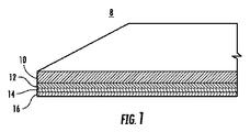
第1実施形態によると、導電性ストリップを使用してメッシュタイプLEDパネルが形成され、この導電性ストリップが、該導電性ストリップの一側面に結合された絶縁性基板を備え、縦方向のストリップが、それ上にある横方向のストリップから分離される。一般的に、ディスプレイとの用語が使用される一方で、当業界においては、LEDディスプレイが、照明デバイスとしても機能することが知られている。従って、“ディスプレイ”との用語が使用される場合、その用語は、この用途において、ディスプレイにおける及び照明デバイスにおけるLEDの使用に及ぶことを意図するものである。図1が、絶縁性基板を有する、LEDパネルに使用するための、導電性ストリップのひとつの型の構造を示す。 According to the first embodiment, a mesh type LED panel is formed using a conductive strip, the conductive strip comprising an insulating substrate bonded to one side of the conductive strip, and the longitudinal strip is Separated from the lateral strips on it. While the term display is generally used, it is known in the art that LED displays also function as lighting devices. Thus, when the term “display” is used, the term is intended to cover the use of LEDs in displays and in lighting devices in this application. FIG. 1 shows one type of structure of a conductive strip for use in an LED panel having an insulating substrate.
図1に示されるように、好ましい実施形態によると、導電性ストリップ8が、導体10、並びに絶縁体14を挟む結合膜12及び16を備える。導電性ストリップが、アルミニウムでめっきされたまたは露出された、真ちゅうまたは銅等のような、任意の導電性材料から形成されてよい。同様に、絶縁体14が、当業者に周知のまたは今後開発される任意の適切な絶縁材料から形成されてよい。
As shown in FIG. 1, according to a preferred embodiment, the conductive strip 8 comprises a
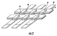
図2は、固定型メッシュを利用する光アレイディスプレイデバイスを備えたLEDパネルの例示的な実施形態を示し、このメッシュが、別個の層内に縦方向及び横方法の導電性ストリップを備えたマトリックスまたはグリッドとして構成され、ストリップの2つの組が、それらの結合部で結合される。図示された実施形態において、図1に示される方法で形成された絶縁構造を有する横方向の導電性ストリップ8が、縦方向の導電性ストリップ20と交点で接続される。この絶縁のために、導電性ストリップ20上を伝わる信号との干渉を生じることなく、導電性ストリップ8が、縦方向の導電性ストリップ20と接触することが可能である。導電性ストリップ20が、アルミニウムでめっきされたまたは露出された、真ちゅうまたは銅等のような、任意の導電性材料から形成されてよいことに留意する。
FIG. 2 illustrates an exemplary embodiment of an LED panel with a light array display device that utilizes a fixed mesh, the mesh comprising longitudinal and lateral conductive strips in separate layers. Or configured as a grid, two sets of strips are joined at their joints. In the illustrated embodiment, a lateral conductive strip 8 having an insulating structure formed by the method shown in FIG. 1 is connected to a longitudinal
導電性ストリップ8及び20の各交点で、LEDパッケージ22が接続される。各交点において、LEDパッケージ22が、はんだ24によって縦方向の導電性ストリップ20と電気的に接続され、はんだ26によって横方向の導電性ストリップ8と電気的に接続される。理解されるように、本発明は、この方法の電気的接続に制限されるものではなく、この接続が、溶接を含むがこれに制限されない当業者に周知である任意の他の方法の電気的接続によって形成されてよい。
An
図2に示される実施形態において、各LEDパッケージ22が、チップボンディングによって横方向の導電性ストリップ8上に設け付けられる。LEDチップの配置が、例えば、手動で、またはピックアンドプレース機によって行われてよい。図3が、光アレイを形成するようにこれらがともに接続される前の部品を示す、図2の実施形態の分解図である。
In the embodiment shown in FIG. 2, each
図4が、固定型メッシュを使用するLED光アレイディスプレイデバイスの第2実施形態を示す。この実施形態において、導電性ストリップ8及び20が、第1実施形態における場合のように、マトリックス状に設けられるが、LED22Aが、ダイ及びワイヤボンディングを使用して、リード30を用いて、このマトリックスに取り付けられる。好ましくは、この実施形態に使用されるLED22Aが、チップ−オン−ボード(COB)型のものである。図に示すように、第2実施形態において、各LED22Aと対応する横方向の導電性ストリップ8との間の電気的接続が、リード30を使用して形成される。LEDパッケージ22Aとそれ上に該LEDパッケージ22Aが設けられる導電性ストリップであって、図示された実施形態においては縦方向の導電性ストリップ20との間の端子接続が、はんだ付け、溶接または電気接続を形成するための当業界において周知の若しくは今後開発される任意の他の方法によって、形成されてよい。第1実施形態における場合ように、チップの配置が、手動で、またはピックアンドプレース機によって行われてよい。
FIG. 4 shows a second embodiment of an LED light array display device using a fixed mesh. In this embodiment, the
図1−4に示される実施形態において、固定型メッシュが、別個の層内において、縦方向及び横方向の導電性ストリップを含むグリッドまたはマトリックスとして構成され、2つの層が、それらの結合部で結合される。 In the embodiment shown in FIGS. 1-4, the stationary mesh is configured as a grid or matrix containing longitudinal and lateral conductive strips in separate layers, and the two layers are at their junction. Combined.
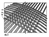
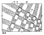
上記のLED光アレイディスプレイデバイスが、図1−4に示された実施形態における固定型メッシュの代わりに、柔軟型メッシュを使用して形成されることも可能である。図5−7に示される第3実施形態において、固定型の実施形態におけるようなLED122用の同じ一般的な接続技術が、用いられることが可能である。例えば、図5及び6が、光アレイデバイスを備えたLEDパネルを示し、より型または編み上げワイヤーから導電性ストリップ108及び120が形成され、銅、真ちゅう、アルミニウム等から形成された複数の導電性の細いワイヤーを含む。このような細いワイヤーが、露出されるまたは導電性材料でコーティングされてよく、この導電性材料が、スズ、ニッケル、銀等を含むが、これに制限されない。柔軟型メッシュの図示された例において、導電性ストリップが、長方形の断面に平坦化された編み上げられた細いワイヤーによって構成される。編み上げ構造を有するストリップを使用することの利点は、これらが、固定ストリップよりもはるかに柔軟であることである。さらなる利点は、いずれの所定の断面に対して、大きな表面積を有し、熱を放散することである。この理由により、編み上げバスが、固定バスよりも低い温度で動作する。さらに、通常、LEDが平坦な底を有するため、平坦化編み上げバスを使用することにより、バス上にLEDを備え付けることを容易にすることが可能である。しかしながら、本発明は、この実施形態に制限されるものではなく、ワイヤーが、円形のより型または編み上げワイヤーであってもよい。
The LED light array display device described above can also be formed using a flexible mesh instead of the stationary mesh in the embodiment shown in FIGS. 1-4. In the third embodiment shown in FIGS. 5-7, the same general connection technology for the
図5及び6から分かるように、あわせて編み上げワイヤーで構成されているプラットフォームを形成する導電性ストリップ108及び120が、導電性ストリップの交点においてLEDパッケージ122に電気的に接続される。第1実施形態における場合のように、各交点において、LEDパッケージ122が、はんだ124によって縦方向の導電性ストリップ120と電気的に接続され、はんだ126によって横方向の導電性ストリップ108と電気的に接続される。固定型メッシュの実施形態における場合と同じように、本発明は、この方法の電気接続に制限されるものではなく、接続が、溶接を含むがこれに制限されない当業者に周知である任意の他の方法の電気接続によって形成されてよい。
As can be seen from FIGS. 5 and 6, the
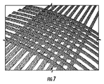
柔軟型メッシュの実施形態において、各LEDパッケージ122が、チップボンディングによって横方向の導電性ストリップ108上に備え付けられる。LEDチップの配置が、例えば、手動でまたはピックアンドプレース機によって実施される。図7は、図5及び6に示される柔軟型メッシュの実施形態の裏面の図である。
In the flexible mesh embodiment, each
図5−7に示された実施形態において、柔軟型メッシュが、別個の層内において、縦方向及び横方向の導電性ストリップを含むマトリックスまたはグリッドとして構成される。柔軟型メッシュの実施形態において、固定型メッシュの実施形態における場合と同じように、層が、それらの結合部で結合されてよく、または、メッシュが、ウィービングによって構成されてもよい。織り形態の場合、各導電性ストリップの基板が、縦方向及び横方向のストリップを互いに分離するように機能する。さらに、織り形態において、2つの導電性ストリップをそれらの結合部で結合する必要はなく、これにより、メッシュに優れた柔軟性を与える。 In the embodiment shown in FIGS. 5-7, the flexible mesh is configured as a matrix or grid containing longitudinal and transverse conductive strips in separate layers. In the flexible mesh embodiment, the layers may be joined at their joints as in the fixed mesh embodiment, or the mesh may be constructed by weaving. In the woven form, the substrate of each conductive strip functions to separate the longitudinal and transverse strips from each other. Furthermore, in the woven form, it is not necessary to join the two conductive strips at their joints, which gives the mesh great flexibility.
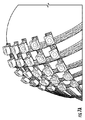
例えば、図7Aに示されるように、上記のような柔軟型メッシュを使用するディスプレイが、球形の物体の形状となることが示される。当業者によって理解されるように、柔軟型メッシュが、他の形状を有することも可能であり、ディスプレイが、例えば、構造上の特徴を有する物の周囲に覆われることが可能となる。 For example, as shown in FIG. 7A, it is shown that the display using the flexible mesh as described above has a shape of a spherical object. As will be appreciated by those skilled in the art, the flexible mesh can have other shapes, allowing the display to be wrapped around an object having structural features, for example.
図1−7Aに図示された実施形態が、各々、単一のカラーLED光アレイを形成する。代替実施形態において、LED光アレイが、多層のグリッドまたはマトリックスを有してよい。例えば、図8に示されるように、4−層のメッシュが構成され、3−色ディスプレイの駆動を可能にする。 The embodiments illustrated in FIGS. 1-7A each form a single color LED light array. In an alternative embodiment, the LED light array may have a multilayer grid or matrix. For example, as shown in FIG. 8, a 4-layer mesh is constructed to allow driving of a 3-color display.
図8において理解されるように、接地、赤色、青色及び緑色ディスプレイ用の駆動信号を伝える導電性ストリップ208、220A、220B及び220Cが、各々、導電性ストリップの交点において、3−色LEDモジュール222のマトリックスに接続される。各LEDパッケージが、全4つの導電性ストリップに接続され、それが対応する特定のピクセルを適切な色にするようにLEDモジュールを駆動させることが可能となる。図8の実施形態において、LEDモジュールが、例えば、4−層メッシュ内において、チップボンディングによって接地ストリップに接続され、並びに、ダイ及びワイヤーボンディングによって3つの層に接続され、接地導体上に備え付けられてよい。
As can be seen in FIG. 8,
単一カラーディスプレイの実施形態に関連する上記の任意のまたは全ての技術を用いることが可能なこのような4−層メッシュを設けることにより、カラーLED光アレイを実現することが可能である。多−層の実施形態において、固定型または柔軟型メッシュが使用されてよく、交点において、制限するものではないが図1−7Aの実施形態に関する上記の方法のような任意の周知の電気的接続方法を用いてよいことに留意する。 By providing such a 4-layer mesh that can use any or all of the techniques described above associated with single color display embodiments, it is possible to realize a color LED light array. In multi-layer embodiments, a fixed or flexible mesh may be used, and any known electrical connection such as, but not limited to, the method described above with respect to the embodiment of FIGS. Note that the method may be used.
好ましい実施形態において、図8に示される4−層構造が、単一のパッケージ内において、3つの−LEDチップから構成されたLEDを使用し、各パッケージがその最下層上に結合される。この最下層が、熱エネルギーを伝導し、電気的な接地を提供するように機能する。他の3つの層が、3つの色を個々に制御するための3つの独立バスを備え、電気伝導及びLEDアドレッシングのために使用される。 In the preferred embodiment, the 4-layer structure shown in FIG. 8 uses LEDs composed of three -LED chips in a single package, with each package bonded onto its bottom layer. This bottom layer functions to conduct thermal energy and provide an electrical ground. The other three layers comprise three independent buses for controlling the three colors individually and are used for electrical conduction and LED addressing.
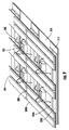
図9に関して、他の多−層型の実施形態が図示される。図9に示されるように、3−層構造が設けられ、各々が、1つのパッケージ322内に3つのLEDチップを備えるLEDが、基板層310上に結合される。好ましくは固定型(またはメッシュ、編み上げ)シート形状を有する基板層が、Cu、Al、Feまたはこれらの合金から形成されることが可能であり、熱エネルギーを伝導するように機能する。3−層構造の他の2つの層が、各々、R、G及びB色制御並びに電気的接地の各1つに対して、2つの独立バスを備え、特に、接地バス308、赤色バス320A、青色バス320B、及び緑色バス320Cである。
With respect to FIG. 9, another multi-layer embodiment is illustrated. As shown in FIG. 9, a three-layer structure is provided, and LEDs each comprising three LED chips in one
図9において理解されるように、この実施形態において、接地バス308と青色バス320Bとが、一方向において、互いに平行に設置され、緑色バス320Cと赤色バス320Aとが、互いに平行に設置され、接地及び青色バスに対して実質的に垂直である。LEDチップが、カラーディスプレイに対して駆動されることが可能となるように、各3つの−LEDチップが、全4つのバスに接続される。絶縁体314が、青色及び接地バスの各組の下に設けられ、一方、他の絶縁体312が、赤色及び緑色バスの各組の下に設けられる。バスが垂直である必要はなく、例えば、制限するものではないが、平行四辺形またはひし形の構造のような他の交差構造を有してよいことに留意すべきである。
As can be seen in FIG. 9, in this embodiment, the
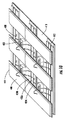
図10は、図9における基板層と同じである基板層410を利用する3−層構造の他の同様な実施形態を示す。図9の3−層構造が、電気的接地バス408に対する単一の層と、3つの色を制御するための3つの独立バス、420A、420B及び420Cを含む他の層と、を提供する。接地に対して用意された単一の層を有することで、接地バスと、R、G、Bカラー用のバスとの間における電流のバランスを上手くとることが出来る。図9及び10における実施形態の両方が、熱及び電気伝導の分離を提供する。
FIG. 10 shows another similar embodiment of a three-layer structure that utilizes a
ディスプレイ駆動を実現するために、LED光アレイ内の各ピクセルが、個々のアドレスに割り当てられることが可能であり、各ピクセルが、マイクロコントローラー及び複数のLED(例えば、3つ(RGB)、または4つ(RGBW)LED)を含むLEDモジュールである。 To achieve display driving, each pixel in the LED light array can be assigned to an individual address, each pixel having a microcontroller and multiple LEDs (eg, 3 (RGB), or 4 LED (RGBW) LED).
上記の実施形態と関連する上記のそれらのようなマトリックスディスプレイにおける使用に適したLEDモジュール500のような実施例が、図11に示されている。このようなLEDモジュールを多数有する例示的なマトリックスが、図12に図示されている。各LEDモジュール500が、:
・1つ以上のLED(R,G,Bまたは任意の他の組み合わせ);
・マイクロコントローラー;
・データポート(DATA);
・4つのI/Oポート、この内の2つが、出力ポート(S0及びS2)であり、この内の2つが、入力ポート(S1及びS3)であるように構成される;
・電源ポート(VCC);及び
・接地ポート(GND)
を備える。
An example of an
One or more LEDs (R, G, B or any other combination);
・ Microcontroller;
-Data port (DATA);
Four I / O ports, two of which are output ports (S0 and S2), two of which are configured to be input ports (S1 and S3);
・ Power supply port (VCC); and ・ Grounding port (GND)
Is provided.
図11及び12において理解されるように、多数のLEDモジュール500が、ディスプレイを形成するようにともに接続される。好ましくは、LEDモジュールが、これらの図面に関連して以下に説明される動的アドレッシングの形式を利用する。動的アドレッシングにおいては、静的アドレッシングのような製造の間のプリセットというよりはむしろ、ピクセルそれ自体によって、ピクセルのアドレスが、動的に割り当てられる。
As can be seen in FIGS. 11 and 12, a number of
好ましくは、各LEDモジュール500が、(a)それ自体のデータポートからデータを受け取り、命令及びグラフィック信号を受け取り、(b)それ上において、動的アドレスシステムに加わるようにそれが配置され、ピクセル(LEDモジュール)に必要な処理を行い、並びに、(c)ともにピクセルを形成するそれ自体のモジュール内のLEDを駆動させる、マイクロコントローラー502を備える。
Preferably, each LED module 500 (a) receives data from its own data port, receives command and graphic signals, and (b) above it is arranged to join the dynamic address system, It comprises a
好ましくは、LEDモジュール500が、以下のように接続される:
・VCC及びGNDポートが、各々、電源と接地バスとの間に接続される。
・DATAポートが、コモンバスに接続される。
・I/OポートS0及びS2が、出力ポートであり、接地されており、I/OポートS1及びS3が、入力ポートであり、VCCに接続されている。隣接するLEDモジュールの入力及び出力ポートが、相互接続されており、メッシュの周囲上において、隣接するLEDモジュールが存在せず、これらが、開放されたままである。メッシュの配線が、図12において図式的な形式で示されている。メッシュの底部右側角における角のLEDモジュールのみが、その出力ポート(S0及びS2)と接続されており、独自に、その2つの入力ポート(S1及びS3)のいずれかと接続されないことに留意する。図示された実施形態において、これは、2つの開放された入力ポートを有するシステムにおけるLEDモジュールのみであり、メッシュに電源が入れられた場合に、LEDモジュールが動的アドレッシングを開始するような、この特定のLEDモジュールを指す。図12に図示された例において、この角のLEDモジュールが、位置No.0,0に割り当てられる。
Preferably, the
VCC and GND ports are each connected between the power supply and the ground bus.
-The DATA port is connected to the common bus.
I / O ports S0 and S2 are output ports and are grounded, and I / O ports S1 and S3 are input ports and are connected to VCC. The input and output ports of adjacent LED modules are interconnected, and there are no adjacent LED modules on the perimeter of the mesh and they remain open. The mesh wiring is shown in schematic form in FIG. Note that only the corner LED module at the bottom right corner of the mesh is connected to its output ports (S0 and S2) and is not uniquely connected to either of its two input ports (S1 and S3). In the illustrated embodiment, this is only the LED module in a system with two open input ports, such that the LED module starts dynamic addressing when the mesh is powered on. Refers to a specific LED module. In the example shown in FIG. Assigned to 0,0.
すなわち、この例において、底部右側の角のLEDモジュールのマイクロコントローラーが、スタートアップ時、リセット時、例えば、または他の時間または周期的に、そのポートのステータスを確認し、接続を有さない(図示された実施形態における開放状態)ような入力ポートのステータスを認識する。これらのポートのステータスから、LEDモジュールのマイクロコントローラーが、それが位置0,0を有し、そのアドレスをそれ自体に割り当てることを認識する。一方で、他のLEDモジュールのマイクロコントローラーが、それらの入力ポートを確認した後で、これらが、接続を有することを認識し、その結果、それら自体のアドレスを0,0として設定しない。 That is, in this example, the bottom right corner LED module microcontroller checks the status of its port at startup, reset, eg, or at other times or periodically, and has no connection (as shown). The status of the input port such as (open state in the embodiment described). From the status of these ports, the LED module's microcontroller recognizes that it has position 0,0 and assigns its address to itself. On the other hand, after the microcontrollers of the other LED modules have recognized their input ports, they will recognize that they have a connection and as a result will not set their own addresses as 0,0.
次に、LEDモジュール0,0のマイクロコントローラーが、その位置を、No.0,0ピクセルとしてその隣接するLEDモジュールに通信し、これによって、その隣接するアドレスをNo.0,1及び1,0に割り当てることにより、動的アドレッシングを開始する。次に、そのように割り当てられたアドレスを有するピクセルが、それらに続く隣接するものと通信し、再帰的なデイジー・チェーンにおいて、図12に示されるようなアドレスを割り当てる。この方法において、各々が、マイクロコントローラーによって制御される個々のピクセルが、電源が入れられた時に、それら自体のアドレスを割り当て、あるピクセルが機能しなくなると、それら自体のアドレスを再度割り当てることが可能である。マイクロコントローラーによって認識されたポートのステータスが、開放状態に制限されず、接続のないことを示すようなマイクロコントローラーによって認識されることが可能ないずれの所定の状態であってよいことに留意すべきである。 Next, the microcontrollers of the LED modules 0 and 0 change their positions to No. Communicates to its adjacent LED module as 0,0 pixels, thereby assigning its adjacent address No. Start dynamic addressing by assigning to 0, 1 and 1, 0. Next, pixels with such assigned addresses communicate with their subsequent neighbors and assign addresses in the recursive daisy chain as shown in FIG. In this way, each individual pixel controlled by the microcontroller can be assigned its own address when powered on and reassign its own address if a pixel fails It is. It should be noted that the status of the port recognized by the microcontroller is not limited to the open state and can be any predetermined state that can be recognized by the microcontroller to indicate no connection. It is.
好ましい実施形態において、全てのLEDモジュール500が、単一のデータラインを共有し、各モジュールが、リモートディスプレイメモリ506に、データ(例えば、表示データ)のリクエストを送信し、ディスプレイコントローラー508によって、データが変更され、リフレッシュされる。
In a preferred embodiment, all
製造の間に各ピクセルが固定されたアドレスに予め−割り当てられる静的アドレッシングによりディスプレイボードを操作する従来型の方法において、特に、ディスプレイにおける形状または解像度についての、任意の変化を監視することは不可能である。動的アドレッシングは、ピクセルが、LEDモジュールにおいて受け取られる信号をベースとしてそれらのアドレッシングを再設定することを可能にするため、これが、設定、維持及び故障検出に関する適応性をもたらすことが可能となる。 In conventional methods of manipulating the display board with static addressing, where each pixel is pre-assigned to a fixed address during manufacturing, it is not possible to monitor any changes, especially for shape or resolution in the display. Is possible. Dynamic addressing allows the pixels to reset their addressing based on signals received at the LED module, which can provide flexibility with respect to setup, maintenance and fault detection.
典型的には、ディスプレイコントローラー508が、ディスプレイメモリ506内の表示データを更新するようにプログラムされ、各ピクセル(LEDモジュール)が、ディスプレイメモリ506からのその各データを取得する。ディスプレイコントローラー508の機能は、ディスプレイメモリを変更し及びリフレッシュすることである。当業者には周知であるように、好ましくは、ディスプレイメモリ506及びディスプレイコントローラー508が、アドレスバス510及びデータバス512の使用により、互いに通信する。
Typically, the
マトリックスディスプレイの動的アドレッシングの上記記載が、好ましい方法であるが、動的アドレッシングを使用するディスプレイの他の駆動方法も可能であり、この方法が、制限されるものではないが、例えば、各LEDモジュールによって受信されるが、コントローラーからの表示命令のアドレスを有するLEDモジュールに作用されるのみである、ディスプレイコントローラーによって送られた表示信号を有することである。 While the above description of dynamic addressing of a matrix display is the preferred method, other driving methods of the display using dynamic addressing are possible and this method is not limited, for example, for each LED Having a display signal sent by the display controller that is received by the module but only acted on the LED module having the address of the display command from the controller.
例えば、図2−7Aに示されるアレイの一つである単一−層メッシュLED光アレイ、または、例えば、図8−10に示されるアレイの一つである多−層メッシュLED光アレイが、配線されてよく、これが、ともに電気的に接続される複数のピクセル(LEDモジュール)を含み、動的ディスプレイを形成する。従来型のディスプレイが、グラフィックコントローラーからディスプレイモジュールへのバースト信号とともに、受動的な方法で作動する。このような従来型のディスプレイにおけるディスプレイコントローラーでは、少なくとも正確なピクセルの数と、ディスプレイモジュールの正確な形状を知ることが要求され、特に、ディスプレイにおける解像度または形状に関する任意の変化を監視することが出来ない。一方、上記のような動的ディスプレイモジュールにおける各ピクセル(LEDモジュール)が、動的ディスプレイにおけるそれ自体のアドレス及び位置を決定するための情報を有する。 For example, a single-layer mesh LED light array that is one of the arrays shown in FIGS. 2-7A, or a multi-layer mesh LED light array that is one of the arrays shown in FIGS. It may be wired and includes a plurality of pixels (LED modules) that are electrically connected together to form a dynamic display. A conventional display operates in a passive manner with a burst signal from the graphics controller to the display module. The display controller in such a conventional display is required to know at least the exact number of pixels and the exact shape of the display module, and in particular can monitor any change in resolution or shape in the display. Absent. On the other hand, each pixel (LED module) in the dynamic display module as described above has information for determining its own address and position in the dynamic display.
上記のように、ピクセル(LEDモジュール)が、ディスプレイユニットのピクセルの数または形状の変化をリアルタイムで監視することが可能であり、その変化に従ってそれ自体のアドレスを再度割り当てる。この固有の特徴を備え、このようなピクセル(LEDモジュール)を備えたディスプレイメッシュが、その構造形状を維持しつつ、多数の小さなディスプレイユニットに分割されることが可能であり、または、大きなディスプレイユニットに統合されることが可能である。各ピクセル(LEDモジュール)のマイクロコントローラーが、例えば、独立して、そのポートの状態に対する変化に気付き、それ自体のアドレスを再度割り当て、対応するディスプレイメモリからのデータを取得することが可能である。 As described above, a pixel (LED module) can monitor changes in the number or shape of the pixels of the display unit in real time and reassign its own address according to the change. A display mesh with this unique feature and with such pixels (LED modules) can be divided into a number of small display units while maintaining its structural shape, or a large display unit Can be integrated. The microcontroller of each pixel (LED module) can, for example, independently notice changes to the state of its port, reassign its own address, and obtain data from the corresponding display memory.
同様に、動的アドレッシングを使用するピクセル(LEDモジュール)が、任意の所望の形状に再度配置されることが可能であり、表示された像が、自動的に、像を変形させることなく、適切な大きさに再度大きさが調節されることが可能である。このことは、ディスプレイコントローラーを再度構成することなくモジュールが他の形状に再度配置される場合に像が変形される従来型のLEDディスプレイモジュールとは対照的である。このようなピクセル(LEDモジュール)が、拡張性のあるテレビの画面のような、拡張性のあるディスプレイスクリーンを形成するために使用されてよい。このような拡張性のあるテレビの画面が、異なるチャンネルまたはプログラムを表示する多数の小さなテレビの画面に分割されてよい。 Similarly, pixels using dynamic addressing (LED modules) can be repositioned in any desired shape, and the displayed image will automatically be appropriate without distorting the image. The size can be adjusted again to the correct size. This is in contrast to conventional LED display modules where the image is deformed when the module is repositioned to another shape without reconfiguring the display controller. Such pixels (LED modules) may be used to form a scalable display screen, such as a scalable television screen. Such a scalable television screen may be divided into a number of small television screens displaying different channels or programs.
照明 illumination
上記実施形態に関連して説明されたLED光アレイを備えたパネルが、正方形、長方形、平行四辺形、またはひし形の形状に構成されてよく、光源光強度に対する要求に適合するように、LEDのピッチが、変更されてよい。本発明によるLED光アレイが、直線的な照明モジュールの使用を必要とする標準的な照明ディスプレイまたは照明器具に使用されてよい。例えば、蛍光灯によって対応されている用途に対し、細長いストリップのようにLED光アレイが配置されてよく、または、つり天井におけるフラッシュ器具に対し、正方形に配置されてもよい。あるいは、LED光アレイが、照明天井または壁の一部または全部のいずれかを形成してもよい。図7Aを参照して上記において示されてように、本発明の柔軟型メッシュの実施形態において、LED光アレイが、カラム型、球形型、スター型及び他の有機的な形状を含みうる構造的効果に対して特別に構成された器具用に使用されてよい。 The panel with the LED light array described in connection with the above embodiments may be configured in a square, rectangular, parallelogram, or rhombus shape, and the LED's so that it meets the requirements for light source light intensity. The pitch may be changed. LED light arrays according to the present invention may be used in standard lighting displays or luminaires that require the use of linear lighting modules. For example, for applications supported by fluorescent lamps, the LED light array may be arranged like an elongated strip, or it may be arranged in a square for a flash fixture in a suspended ceiling. Alternatively, the LED light array may form either the lighting ceiling or part or all of the wall. As shown above with reference to FIG. 7A, in the flexible mesh embodiment of the present invention, the LED light array can include columnar, spherical, star and other organic shapes. It may be used for instruments specially configured for effect.
本発明の2−層型の実施形態が、固定された単一または多色の用途のために使用されてよい。本発明の多−層実施形態が、フルまたは可変カラー用途に使用されうる多数のLED(例えば、赤、青及び緑の3つのLED)、または単一色のLEDを有してよい。 The two-layer embodiment of the present invention may be used for fixed single or multicolor applications. Multi-layer embodiments of the present invention may have multiple LEDs that can be used for full or variable color applications (eg, three LEDs, red, blue and green), or single color LEDs.
ディスプレイスクリーン Display screen
上記の動的アドレッシングシステムを備える、LED光アレイの多−層メッシュ構造が、大きなテレビの画面または“テレビジョンウォール”を含む動的ディスプレイスクリーンの構成に使用されてよい。同一の個々のメッシュが、共に備え付けられてよく、各ピクセル(マイクロコントローラー及び複数のLED(例えば3つ(RGB)または4つ(RGBW)LED)を備える)の固有のアドレスが、動的に割り当てられてる。 A multi-layer mesh structure of an LED light array comprising the dynamic addressing system described above may be used to construct a dynamic display screen including a large television screen or “television wall”. The same individual mesh may be provided together, and a unique address for each pixel (including a microcontroller and multiple LEDs (eg, comprising 3 (RGB) or 4 (RGBW) LEDs)) is dynamically assigned. It ’s been.
特定の実施形態が、図示され、本明細書において説明されたが、本発明の範囲を逸脱することなく、種々の代替の及び/または同等な実施が、示され及び説明された特定の実施形態を代替しうることが当業者によって理解されるだろう。本出願は、本明細書において議論された特定の実施形態を任意に変更したものまたは適応させたものに及ぶことを意図している。従って、本発明は、特許請求の範囲及びその同等なものによってのみ限定されることが意図される。 While specific embodiments have been illustrated and described herein, various alternative and / or equivalent implementations have been shown and described without departing from the scope of the invention. One skilled in the art will appreciate that can be substituted. This application is intended to cover any variations or adaptations of the specific embodiments discussed herein. Therefore, it is intended that this invention be limited only by the claims and the equivalents thereof.
8 導電性ストリップ
10 導体
12 結合膜
14 絶縁体
16 結合膜
20 導電性ストリップ
22 LEDパッケージ
24 はんだ
26 はんだ
Claims (22)
第2方向に配置された第2の複数の編み上げワイヤー導電性ストリップと、
複数の発光ダイオード(LED)モジュールと、
を備えた柔軟型メッシュディスプレイデバイスであって、
前記第1の複数の導電性ストリップと前記第2の複数の導電性ストリップとが、その間に複数の交点を形成し、
前記各LEDモジュールが、前記ディスプレイデバイスのピクセルを形成し、
前記複数のLEDモジュールの各々が、前記複数の交点の1つに配置され、
前記各LEDモジュールが、前記編み上げワイヤー導電性ストリップの少なくとも1つから表示信号を受け取り、受け取った前記信号に従って光を表示するように構成されることを特徴とする柔軟型メッシュディスプレイデバイス。 A first plurality of braided wire conductive strips disposed in a first direction;
A second plurality of braided wire conductive strips disposed in a second direction;
A plurality of light emitting diode (LED) modules;
A flexible mesh display device comprising:
The first plurality of conductive strips and the second plurality of conductive strips form a plurality of intersections therebetween,
Each LED module forms a pixel of the display device;
Each of the plurality of LED modules is disposed at one of the plurality of intersections;
A flexible mesh display device, wherein each LED module is configured to receive a display signal from at least one of the braided wire conductive strips and to display light according to the received signal.
前記マイクロコントローラーが、
前記1つ以上のポートの少なくとも1つのステータスを確認し、
前記ポートのステータスが、所定の状態と対応する場合、
前記マイクロコントローラーが属するLEDモジュールに、第1ディスプレイアドレスを割り当て、
前記ディスプレイデバイス内のLEDモジュールの他のLEDモジュールのマイクロコントローラーに信号を送り、前記信号が、前記ディスプレイデバイス内のLEDモジュールの前記他のLEDモジュールに、各々のさらなるディスプレイアドレスを割り当てるように構成されることを特徴とする請求項1に記載の柔軟型メッシュディスプレイデバイス。 Each LED module includes a microcontroller and one or more ports;
The microcontroller is
Check the status of at least one of the one or more ports;
When the status of the port corresponds to a predetermined state,
Assign a first display address to the LED module to which the microcontroller belongs,
Sending a signal to a microcontroller of another LED module in the LED module in the display device, the signal being configured to assign each further display address to the other LED module in the LED module in the display device. The flexible mesh display device according to claim 1.
前記ディスプレイメモリ内に保存された前記情報が、前記LEDモジュールの前記各マイクロコントローラーによってアクセスされることが可能であり、前記マイクロコントローラーが、表示のための最新の情報を読み出すことが可能であることを特徴とする請求項4に記載の柔軟型メッシュディスプレイデバイス。 A display memory for storing the latest display information related to the pixel address of the display;
The information stored in the display memory can be accessed by each microcontroller of the LED module, and the microcontroller can read the latest information for display. The flexible mesh display device according to claim 4.
前記ディスプレイコントローラーが、前記ディスプレイメモリ内に保存された前記表示情報を更新するように構成されることを特徴とする請求項5に記載の柔軟型メッシュディスプレイデバイス。 A display controller,
The flexible mesh display device of claim 5, wherein the display controller is configured to update the display information stored in the display memory.
直接的または間接的に前記第1層と接触するように配置された第2層であって、R,G及びB色制御並びに電気的接地の少なくとも1つを制御するための第1方向に配置された1つ以上の第2層独立バスを備えた第2層と、
前記第1方向と異なる第2方向に配置された1つ以上の第3層独立バスを備えた第3層と、
複数の発光ダイオード(LED)モジュールと、
を備えた多−層ディスプレイデバイスであって、
前記第3層独立バスが、前記第2層独立バスによっては制御されない前記R,G及びB色制御並びに電気的接地の少なくとも1つを制御し、
前記各モジュールが、前記ディスプレイデバイスのピクセルを形成し、
前記複数のLEDモジュールの各々が、前記第1層上に備え付けられ、
前記各LEDモジュールが、前記第2層独立バス及び前記第3層独立バスの少なくとも1つから表示信号を受けとり、受けとった前記信号に従って光を表示するように構成されることを特徴とする多−層ディスプレイデバイス。 A first layer comprising a substrate layer conducting at least thermal energy;
A second layer disposed in direct or indirect contact with the first layer and disposed in a first direction for controlling at least one of R, G and B color control and electrical grounding A second tier with one or more second tier independent buses formed;
A third layer comprising one or more third layer independent buses arranged in a second direction different from the first direction;
A plurality of light emitting diode (LED) modules;
A multi-layer display device comprising:
The third layer independent bus controls at least one of the R, G and B color controls and electrical ground not controlled by the second layer independent bus;
Each module forms a pixel of the display device;
Each of the plurality of LED modules is provided on the first layer;
Each of the LED modules is configured to receive a display signal from at least one of the second layer independent bus and the third layer independent bus and to display light according to the received signal. Layer display device.
前記第3層が、電気的接地のための前記独立バスを備えることを特徴とする請求項12に記載の多−層ディスプレイデバイス。 The second layer comprises the independent bus for R, G and B color control;
The multi-layer display device of claim 12, wherein the third layer comprises the independent bus for electrical grounding.
前記第3層が、電気的接地のための前記独立バスと、前記第2層内に配置されない色制御のための前記独立バスと、を備えることを特徴とする請求項12に記載の多−層ディスプレイデバイス。 The second layer comprises the independent bus for two of the R, G and B color controls;
The multi-layer according to claim 12, wherein the third layer comprises the independent bus for electrical grounding and the independent bus for color control not disposed in the second layer. Layer display device.
前記マイクロコントローラーが、
前記1つ以上のポートの少なくとも1つのステータスを確認し、
前記ポートのステータスが、所定の状態と対応する場合、
前記マイクロコントローラーが属するLEDモジュールに、第1ディスプレイアドレスを割り当て、
前記ディスプレイデバイス内のLEDモジュールの他のLEDモジュールのマイクロコントローラーに信号を送り、前記信号が、前記ディスプレイデバイス内の前記他のLEDモジュールに、各々のさらなるディスプレイアドレスを割り当てるように構成されることを特徴とする請求項12に記載の多−層ディスプレイデバイス。 Each LED module comprises a microcontroller and one or more ports;
The microcontroller is
Check the status of at least one of the one or more ports;
When the status of the port corresponds to a predetermined state,
Assign a first display address to the LED module to which the microcontroller belongs,
Sending a signal to a microcontroller of another LED module in the LED module in the display device, the signal being configured to assign each further display address to the other LED module in the display device. The multi-layer display device according to claim 12, characterized in that:
前記ディスプレイメモリ内に保存された前記情報が、前記LEDモジュールの前記各マイクロコントローラーからアクセスされることが可能であり、前記マイクロコントローラーが、表示のための最新の情報を読み出すことが可能であることを特徴とする請求項15に記載の柔軟型メッシュディスプレイデバイス。 A display memory for storing the latest display information related to the pixel address of the display;
The information stored in the display memory can be accessed from the respective microcontrollers of the LED module, and the microcontroller can read the latest information for display. The flexible mesh display device according to claim 15.
前記ディスプレイコントローラーが、前記ディスプレイメモリ内に保存された前記表示情報を更新するように構成されることを特徴とする請求項16に記載の多−層ディスプレイデバイス。 A display controller,
The multi-layer display device of claim 16, wherein the display controller is configured to update the display information stored in the display memory.
前記各LEDモジュールが、
1つ以上のLEDと、
マイクロコントローラーと、
1つ以上のポートと、
を含み、
前記マイクロコントローラーが、
前記1つ以上のポートの少なくとも1つのステータスを確認し、
前記ポートのステータスが、所定の状態と対応する場合、
前記マイクロコントローラーが属するLEDモジュールに、第1ディスプレイアドレスを割り当て、
前記ディスプレイデバイス内のLEDモジュールの他のLEDモジュールのマイクロコントローラーに信号を送り、前記信号が、前記LEDデバイス内の前記他のLEDモジュールに、各々のさらなるディスプレイアドレスを割り当てるように構成され、
前記ディスプレイメモリが、前記LEDデバイス内の前記各LEDモジュールに対する最新の表示ステータスを保存することを特徴とするLEDデバイス。 A light emitting diode (LED) device comprising: (a) a plurality of LED modules; and (b) a display memory coupled to the plurality of LED modules.
Each LED module is
One or more LEDs;
A microcontroller,
One or more ports,
Including
The microcontroller is
Check the status of at least one of the one or more ports;
When the status of the port corresponds to a predetermined state,
Assign a first display address to the LED module to which the microcontroller belongs,
Sending a signal to a microcontroller of another LED module in the LED module in the display device, the signal being configured to assign each further display address to the other LED module in the LED device;
The LED device, wherein the display memory stores a latest display status for each LED module in the LED device.
Applications Claiming Priority (3)
| Application Number | Priority Date | Filing Date | Title |
|---|---|---|---|
| US15114309P | 2009-02-09 | 2009-02-09 | |
| US61/151,143 | 2009-02-09 | ||
| PCT/EP2010/051557 WO2010089409A1 (en) | 2009-02-09 | 2010-02-09 | Light emitting diode light arrays on mesh platforms |
Related Child Applications (1)
| Application Number | Title | Priority Date | Filing Date |
|---|---|---|---|
| JP2013027524A Division JP2013101396A (en) | 2009-02-09 | 2013-02-15 | Light emitting diode optical array on mesh platform |
Publications (2)
| Publication Number | Publication Date |
|---|---|
| JP2012508404A true JP2012508404A (en) | 2012-04-05 |
| JP5442027B2 JP5442027B2 (en) | 2014-03-12 |
Family
ID=42084591
Family Applications (2)
| Application Number | Title | Priority Date | Filing Date |
|---|---|---|---|
| JP2011543781A Expired - Fee Related JP5442027B2 (en) | 2009-02-09 | 2010-02-09 | Light Emitting Diode Light Array on Mesh Platform |
| JP2013027524A Pending JP2013101396A (en) | 2009-02-09 | 2013-02-15 | Light emitting diode optical array on mesh platform |
Family Applications After (1)
| Application Number | Title | Priority Date | Filing Date |
|---|---|---|---|
| JP2013027524A Pending JP2013101396A (en) | 2009-02-09 | 2013-02-15 | Light emitting diode optical array on mesh platform |
Country Status (13)
| Country | Link |
|---|---|
| US (1) | US20100201610A1 (en) |
| EP (1) | EP2340475A1 (en) |
| JP (2) | JP5442027B2 (en) |
| KR (1) | KR101242902B1 (en) |
| CN (2) | CN202142051U (en) |
| AU (1) | AU2010210080B2 (en) |
| BR (1) | BRPI1005174A2 (en) |
| CA (1) | CA2740705C (en) |
| HK (1) | HK1155901A2 (en) |
| MX (1) | MX2011004041A (en) |
| TW (1) | TW201104653A (en) |
| WO (1) | WO2010089409A1 (en) |
| ZA (1) | ZA201102480B (en) |
Cited By (3)
| Publication number | Priority date | Publication date | Assignee | Title |
|---|---|---|---|---|
| KR20150022399A (en) * | 2013-08-23 | 2015-03-04 | 삼성디스플레이 주식회사 | Display device |
| JP2016539513A (en) * | 2013-11-05 | 2016-12-15 | フィリップス ライティング ホールディング ビー ヴィ | Conductive textile device |
| WO2023158129A1 (en) * | 2022-02-16 | 2023-08-24 | 한국에이치엠아이(주) | Display equipment |
Families Citing this family (38)
| Publication number | Priority date | Publication date | Assignee | Title |
|---|---|---|---|---|
| RU2011111366A (en) * | 2011-03-28 | 2012-10-10 | Святослав Иванович Арсенич (RU) | MATRIX INDICATOR (OPTIONS) AND METHOD FOR ITS MANUFACTURE |
| JP2012256558A (en) * | 2011-06-10 | 2012-12-27 | Meitaku Kogyo Kk | Large-size surface light source device |
| CN202217456U (en) * | 2011-08-12 | 2012-05-09 | 广州市夜空彩虹光电科技有限公司 | Light emitting diode (LED) flexible hung display screen |
| TWI443279B (en) * | 2012-03-05 | 2014-07-01 | Lextar Electronics Corp | Stretchable light-emitting module |
| WO2013156883A2 (en) * | 2012-04-19 | 2013-10-24 | Koninklijke Philips N.V. | A led grid device and a method of manufacturing a led grid device |
| TWI490837B (en) * | 2012-10-19 | 2015-07-01 | 啟耀光電股份有限公司 | Display apparatus |
| US9153171B2 (en) * | 2012-12-17 | 2015-10-06 | LuxVue Technology Corporation | Smart pixel lighting and display microcontroller |
| DE102013114691A1 (en) | 2013-12-20 | 2015-06-25 | Osram Opto Semiconductors Gmbh | Optoelectronic semiconductor component and adaptive headlight for a motor vehicle |
| US20160180821A1 (en) * | 2014-12-23 | 2016-06-23 | Intel Corporation | Distributed memory panel |
| CN111261639A (en) * | 2015-09-11 | 2020-06-09 | 夏普株式会社 | Image display device and method of manufacturing image display element |
| CN105114920A (en) * | 2015-09-17 | 2015-12-02 | 张逸兴 | Device capable of exchanging heat by using heat conduction material wire rod braided fabric |
| DE102016114319B4 (en) * | 2016-08-03 | 2019-02-28 | Inteca Gmbh | Flat lighting device |
| KR102482334B1 (en) * | 2016-08-04 | 2022-12-29 | 삼성디스플레이 주식회사 | Display device |
| WO2018075998A1 (en) * | 2016-10-23 | 2018-04-26 | A Zykin | Ls grid core led connector system and manufacturing method |
| CN107481628A (en) * | 2017-08-30 | 2017-12-15 | 深圳市软屏光电有限公司 | Soft module of spherical LED display screen |
| CN109956517A (en) * | 2017-12-14 | 2019-07-02 | 丰田合成株式会社 | Ultraviolet light sterilizing unit and fluid sterilizing unit |
| JP7035499B2 (en) * | 2017-12-14 | 2022-03-15 | 豊田合成株式会社 | Ultraviolet light irradiation sterilizer |
| KR102136921B1 (en) * | 2018-03-02 | 2020-07-28 | 주식회사 루멘스 | Flexible display apparatus attached on outer panel of vehicle |
| CA3050232A1 (en) * | 2018-09-11 | 2020-03-11 | Andrew Cook | Ceiling system and hanger for suspending ceiling tiles or panels therefrom |
| CN109335445B (en) * | 2018-10-13 | 2020-06-16 | 晋江易库物联网科技有限公司 | A kind of goods scheduling method for intelligent warehouse |
| US11727857B2 (en) | 2019-03-29 | 2023-08-15 | Creeled, Inc. | Active control of light emitting diodes and light emitting diode displays |
| US11694601B2 (en) | 2019-03-29 | 2023-07-04 | Creeled, Inc. | Active control of light emitting diodes and light emitting diode displays |
| US12142716B2 (en) | 2019-03-29 | 2024-11-12 | Creeled, Inc. | Active control of light emitting diodes and light emitting diode displays |
| US12198605B2 (en) | 2019-03-29 | 2025-01-14 | Creeled, Inc. | Active control of light emitting diodes and light emitting diode displays |
| KR102891288B1 (en) * | 2019-10-08 | 2025-11-25 | 엘지디스플레이 주식회사 | Display device |
| CN115148171B (en) * | 2019-10-09 | 2024-07-30 | 群创光电股份有限公司 | Electronic device |
| WO2021251613A1 (en) | 2020-06-12 | 2021-12-16 | 삼성전자주식회사 | Display device and control method therefor |
| KR102504013B1 (en) * | 2020-06-12 | 2023-02-28 | 삼성전자주식회사 | Display apparatus and control method thereof |
| US10909911B1 (en) * | 2020-09-18 | 2021-02-02 | Huayuan Semiconductor (Shenzhen) Limited Company | Display device with distributed driver circuits and shared multi-wire communication interface for dimming data |
| WO2022107321A1 (en) * | 2020-11-20 | 2022-05-27 | 三菱電機株式会社 | Display panel, display device, and method for manufacturing display panel |
| MX2023009721A (en) * | 2021-02-18 | 2023-11-10 | Paul Dorland | LED DISPLAY SYSTEM. |
| CN113013119B (en) * | 2021-03-03 | 2022-07-12 | 同辉电子科技股份有限公司 | LED chip with array structure |
| WO2023150502A1 (en) | 2022-02-07 | 2023-08-10 | Creeled, Inc. | Light-emitting diodes with mixed clock domain signaling |
| CN117396644A (en) * | 2022-04-20 | 2024-01-12 | 京东方科技集团股份有限公司 | Display panels and display devices |
| US12618917B2 (en) | 2022-11-15 | 2026-05-05 | Creeled, Inc. | Error detection in LED packages |
| US12014677B1 (en) | 2023-04-10 | 2024-06-18 | Creeled, Inc. | Light-emitting diode packages with transformation and shifting of pulse width modulation signals and related methods |
| US12526889B2 (en) | 2023-08-29 | 2026-01-13 | Creeled, Inc. | Light-emitting diode packages with varying current pulse width modulation and related methods |
| US12437707B2 (en) | 2023-09-27 | 2025-10-07 | Creeled, Inc. | Pseudo-exponential encoding for light-emitting devices and related methods |
Citations (16)
| Publication number | Priority date | Publication date | Assignee | Title |
|---|---|---|---|---|
| JPS6243689A (en) * | 1985-08-20 | 1987-02-25 | タキロン株式会社 | Dot matrix light emitting display body |
| JPS62160562U (en) * | 1986-03-31 | 1987-10-13 | ||
| JPH01162382U (en) * | 1988-04-28 | 1989-11-13 | ||
| JPH0572978A (en) * | 1991-09-17 | 1993-03-26 | Denki Kagaku Kogyo Kk | Flexible matrix circuit board and display board |
| JPH07219452A (en) * | 1994-02-01 | 1995-08-18 | Hitachi Media Electron:Kk | LED display device |
| JPH0836367A (en) * | 1994-07-22 | 1996-02-06 | Hitachi Media Electron:Kk | LED display device |
| JPH08202289A (en) * | 1995-01-31 | 1996-08-09 | Mitsubishi Cable Ind Ltd | Multicolor display device |
| JP2000012906A (en) * | 1998-06-17 | 2000-01-14 | Kasuto:Kk | Display device |
| JP2000221934A (en) * | 1999-01-29 | 2000-08-11 | Nichia Chem Ind Ltd | Led display device and control method thereof using the same |
| JP2002093206A (en) * | 2000-09-18 | 2002-03-29 | Stanley Electric Co Ltd | LED signal light |
| JP2004354852A (en) * | 2003-05-30 | 2004-12-16 | Natsume Kk | Externally controlled tubular light emitting device and lightning display |
| JP2005524783A (en) * | 2002-05-10 | 2005-08-18 | サーノフ・コーポレーション | Electronic woven fabric, yarn and fabric |
| JP2005525481A (en) * | 2002-05-10 | 2005-08-25 | サーノフ・コーポレーション | Electronic woven fabric having multiple layers, woven fabric and method of woven it |
| JP2006500765A (en) * | 2002-08-26 | 2006-01-05 | シーエッチ キャピタル インコーポレイテッド | Electronic assembly / system with reduced cost, mass, volume and increased efficiency and power density |
| JP2007163992A (en) * | 2005-12-15 | 2007-06-28 | Maeda Kosen Co Ltd | Flexible sheet display |
| JP2009538440A (en) * | 2006-05-24 | 2009-11-05 | コーニンクレッカ フィリップス エレクトロニクス エヌ ヴィ | Method and apparatus for automatic commissioning of LED-based display configurations |
Family Cites Families (9)
| Publication number | Priority date | Publication date | Assignee | Title |
|---|---|---|---|---|
| JPH088463A (en) * | 1994-06-21 | 1996-01-12 | Sharp Corp | Thin LED dot matrix unit |
| JP2847360B2 (en) * | 1996-08-09 | 1999-01-20 | 岡谷電機産業株式会社 | LED display |
| JP4403434B2 (en) * | 2000-07-18 | 2010-01-27 | ソニー株式会社 | Image display device |
| US7324071B2 (en) * | 2003-09-16 | 2008-01-29 | Sarnoff Corporation | Segmented character display |
| US20080196783A1 (en) * | 2005-05-31 | 2008-08-21 | Koninklijke Philips Electronics, N.V. | Fully Textile Electrode Lay-Out Allowing Passive and Active Matrix Addressing |
| CA2567113A1 (en) * | 2006-05-16 | 2007-11-16 | Tribar Industries Inc. | Large scale flexible led video display and control system therefor |
| DE102006037878A1 (en) * | 2006-08-11 | 2008-02-14 | Haver & Boecker Ohg | Illuminated fabric and method for its production |
| EP2132725A1 (en) * | 2007-03-08 | 2009-12-16 | Element Labs, Inc. | Ladder display system |
| US7729570B2 (en) * | 2007-05-18 | 2010-06-01 | Ibiden Co., Ltd. | Photoelectric circuit board and device for optical communication |
-
2010
- 2010-02-09 CA CA2740705A patent/CA2740705C/en not_active Expired - Fee Related
- 2010-02-09 BR BRPI1005174A patent/BRPI1005174A2/en not_active IP Right Cessation
- 2010-02-09 CN CN2010900005814U patent/CN202142051U/en not_active Expired - Lifetime
- 2010-02-09 EP EP10708742A patent/EP2340475A1/en not_active Withdrawn
- 2010-02-09 KR KR1020117008506A patent/KR101242902B1/en not_active Expired - Fee Related
- 2010-02-09 AU AU2010210080A patent/AU2010210080B2/en not_active Ceased
- 2010-02-09 MX MX2011004041A patent/MX2011004041A/en active IP Right Grant
- 2010-02-09 WO PCT/EP2010/051557 patent/WO2010089409A1/en not_active Ceased
- 2010-02-09 US US12/702,979 patent/US20100201610A1/en not_active Abandoned
- 2010-02-09 CN CN2011204501491U patent/CN202650448U/en not_active Expired - Lifetime
- 2010-02-09 TW TW099103939A patent/TW201104653A/en unknown
- 2010-02-09 JP JP2011543781A patent/JP5442027B2/en not_active Expired - Fee Related
- 2010-02-09 HK HK11105079.0A patent/HK1155901A2/en not_active IP Right Cessation
-
2011
- 2011-04-04 ZA ZA2011/02480A patent/ZA201102480B/en unknown
-
2013
- 2013-02-15 JP JP2013027524A patent/JP2013101396A/en active Pending
Patent Citations (16)
| Publication number | Priority date | Publication date | Assignee | Title |
|---|---|---|---|---|
| JPS6243689A (en) * | 1985-08-20 | 1987-02-25 | タキロン株式会社 | Dot matrix light emitting display body |
| JPS62160562U (en) * | 1986-03-31 | 1987-10-13 | ||
| JPH01162382U (en) * | 1988-04-28 | 1989-11-13 | ||
| JPH0572978A (en) * | 1991-09-17 | 1993-03-26 | Denki Kagaku Kogyo Kk | Flexible matrix circuit board and display board |
| JPH07219452A (en) * | 1994-02-01 | 1995-08-18 | Hitachi Media Electron:Kk | LED display device |
| JPH0836367A (en) * | 1994-07-22 | 1996-02-06 | Hitachi Media Electron:Kk | LED display device |
| JPH08202289A (en) * | 1995-01-31 | 1996-08-09 | Mitsubishi Cable Ind Ltd | Multicolor display device |
| JP2000012906A (en) * | 1998-06-17 | 2000-01-14 | Kasuto:Kk | Display device |
| JP2000221934A (en) * | 1999-01-29 | 2000-08-11 | Nichia Chem Ind Ltd | Led display device and control method thereof using the same |
| JP2002093206A (en) * | 2000-09-18 | 2002-03-29 | Stanley Electric Co Ltd | LED signal light |
| JP2005524783A (en) * | 2002-05-10 | 2005-08-18 | サーノフ・コーポレーション | Electronic woven fabric, yarn and fabric |
| JP2005525481A (en) * | 2002-05-10 | 2005-08-25 | サーノフ・コーポレーション | Electronic woven fabric having multiple layers, woven fabric and method of woven it |
| JP2006500765A (en) * | 2002-08-26 | 2006-01-05 | シーエッチ キャピタル インコーポレイテッド | Electronic assembly / system with reduced cost, mass, volume and increased efficiency and power density |
| JP2004354852A (en) * | 2003-05-30 | 2004-12-16 | Natsume Kk | Externally controlled tubular light emitting device and lightning display |
| JP2007163992A (en) * | 2005-12-15 | 2007-06-28 | Maeda Kosen Co Ltd | Flexible sheet display |
| JP2009538440A (en) * | 2006-05-24 | 2009-11-05 | コーニンクレッカ フィリップス エレクトロニクス エヌ ヴィ | Method and apparatus for automatic commissioning of LED-based display configurations |
Cited By (4)
| Publication number | Priority date | Publication date | Assignee | Title |
|---|---|---|---|---|
| KR20150022399A (en) * | 2013-08-23 | 2015-03-04 | 삼성디스플레이 주식회사 | Display device |
| KR102179971B1 (en) * | 2013-08-23 | 2020-11-18 | 삼성디스플레이 주식회사 | Display device |
| JP2016539513A (en) * | 2013-11-05 | 2016-12-15 | フィリップス ライティング ホールディング ビー ヴィ | Conductive textile device |
| WO2023158129A1 (en) * | 2022-02-16 | 2023-08-24 | 한국에이치엠아이(주) | Display equipment |
Also Published As
| Publication number | Publication date |
|---|---|
| CA2740705A1 (en) | 2010-08-12 |
| JP5442027B2 (en) | 2014-03-12 |
| TW201104653A (en) | 2011-02-01 |
| KR101242902B1 (en) | 2013-03-13 |
| KR20110082137A (en) | 2011-07-18 |
| AU2010210080A1 (en) | 2010-08-12 |
| BRPI1005174A2 (en) | 2017-06-13 |
| ZA201102480B (en) | 2012-01-25 |
| EP2340475A1 (en) | 2011-07-06 |
| MX2011004041A (en) | 2011-07-29 |
| JP2013101396A (en) | 2013-05-23 |
| CN202650448U (en) | 2013-01-02 |
| AU2010210080A8 (en) | 2011-06-02 |
| WO2010089409A8 (en) | 2010-11-11 |
| AU2010210080B2 (en) | 2012-09-20 |
| CA2740705C (en) | 2013-01-15 |
| WO2010089409A1 (en) | 2010-08-12 |
| US20100201610A1 (en) | 2010-08-12 |
| HK1155901A2 (en) | 2012-05-25 |
| CN202142051U (en) | 2012-02-08 |
Similar Documents
| Publication | Publication Date | Title |
|---|---|---|
| JP5442027B2 (en) | Light Emitting Diode Light Array on Mesh Platform | |
| JP5559834B2 (en) | Backlight using LED and liquid crystal display device including the same | |
| US8567992B2 (en) | Integrally formed light emitting diode light wire and uses thereof | |
| JP6533624B2 (en) | LED light emitting unit, LED light emitting panel and LED display screen | |
| CN112863386B (en) | Backlight module and display device | |
| TWI394914B (en) | Integrally formed single piece light emitting diode light wire and uses thereof | |
| EP2050090B1 (en) | Electroluminescent display having a pixel array | |
| JP2019091032A (en) | LED display device | |
| WO2021184810A1 (en) | Led lamp bead and led display structure | |
| CN110224015B (en) | Organic light emitting diode panel and OLED light emitting device | |
| JP7288080B2 (en) | Components for display devices, display devices and methods of operating display devices | |
| JP2018087927A (en) | LED display device | |
| TW201002977A (en) | LED lamp | |
| AU2012241114A1 (en) | Light emitting diode light arrays on mesh platforms | |
| JP3210218U (en) | Signage equipment | |
| CN111354763A (en) | Electroluminescent lighting device | |
| CN221008580U (en) | Grid type LED display screen | |
| CN121415691A (en) | A transparent display module and a transparent display screen | |
| JP2018088491A (en) | LED display device | |
| KR102309511B1 (en) | Liquid crystal display device | |
| JP2008016477A (en) | Light emitting diode display device | |
| JP2004177724A (en) | Flat screen monitor | |
| HK1171322B (en) | Integrally formed light emitting diode light wire and uses thereof | |
| JPH03219280A (en) | Display unit |
Legal Events
| Date | Code | Title | Description |
|---|---|---|---|
| A977 | Report on retrieval |
Free format text: JAPANESE INTERMEDIATE CODE: A971007 Effective date: 20121012 |
|
| A131 | Notification of reasons for refusal |
Free format text: JAPANESE INTERMEDIATE CODE: A131 Effective date: 20121016 |
|
| A601 | Written request for extension of time |
Free format text: JAPANESE INTERMEDIATE CODE: A601 Effective date: 20130116 |
|
| A602 | Written permission of extension of time |
Free format text: JAPANESE INTERMEDIATE CODE: A602 Effective date: 20130123 |
|
| A521 | Request for written amendment filed |
Free format text: JAPANESE INTERMEDIATE CODE: A523 Effective date: 20130215 |
|
| A131 | Notification of reasons for refusal |
Free format text: JAPANESE INTERMEDIATE CODE: A131 Effective date: 20130702 |
|
| A521 | Request for written amendment filed |
Free format text: JAPANESE INTERMEDIATE CODE: A523 Effective date: 20131002 |
|
| TRDD | Decision of grant or rejection written | ||
| A01 | Written decision to grant a patent or to grant a registration (utility model) |
Free format text: JAPANESE INTERMEDIATE CODE: A01 Effective date: 20131119 |
|
| A61 | First payment of annual fees (during grant procedure) |
Free format text: JAPANESE INTERMEDIATE CODE: A61 Effective date: 20131217 |
|
| R150 | Certificate of patent or registration of utility model |
Free format text: JAPANESE INTERMEDIATE CODE: R150 |
|
| R250 | Receipt of annual fees |
Free format text: JAPANESE INTERMEDIATE CODE: R250 |
|
| LAPS | Cancellation because of no payment of annual fees |