JP2012509397A - タッチパネルディスプレイとともに使用するためのito被覆品の製造方法、および/または前記ito被覆品の製造方法 - Google Patents
タッチパネルディスプレイとともに使用するためのito被覆品の製造方法、および/または前記ito被覆品の製造方法 Download PDFInfo
- Publication number
- JP2012509397A JP2012509397A JP2011536361A JP2011536361A JP2012509397A JP 2012509397 A JP2012509397 A JP 2012509397A JP 2011536361 A JP2011536361 A JP 2011536361A JP 2011536361 A JP2011536361 A JP 2011536361A JP 2012509397 A JP2012509397 A JP 2012509397A
- Authority
- JP
- Japan
- Prior art keywords
- film
- ito
- indium tin
- substrate
- sputtering
- Prior art date
- Legal status (The legal status is an assumption and is not a legal conclusion. Google has not performed a legal analysis and makes no representation as to the accuracy of the status listed.)
- Pending
Links
Images


Classifications
-
- C—CHEMISTRY; METALLURGY
- C03—GLASS; MINERAL OR SLAG WOOL
- C03C—CHEMICAL COMPOSITION OF GLASSES, GLAZES OR VITREOUS ENAMELS; SURFACE TREATMENT OF GLASS; SURFACE TREATMENT OF FIBRES OR FILAMENTS MADE FROM GLASS, MINERALS OR SLAGS; JOINING GLASS TO GLASS OR OTHER MATERIALS
- C03C17/00—Surface treatment of glass, not in the form of fibres or filaments, by coating
- C03C17/22—Surface treatment of glass, not in the form of fibres or filaments, by coating with other inorganic material
- C03C17/23—Oxides
- C03C17/245—Oxides by deposition from the vapour phase
- C03C17/2456—Coating containing TiO2
-
- C—CHEMISTRY; METALLURGY
- C23—COATING METALLIC MATERIAL; COATING MATERIAL WITH METALLIC MATERIAL; CHEMICAL SURFACE TREATMENT; DIFFUSION TREATMENT OF METALLIC MATERIAL; COATING BY VACUUM EVAPORATION, BY SPUTTERING, BY ION IMPLANTATION OR BY CHEMICAL VAPOUR DEPOSITION, IN GENERAL; INHIBITING CORROSION OF METALLIC MATERIAL OR INCRUSTATION IN GENERAL
- C23C—COATING METALLIC MATERIAL; COATING MATERIAL WITH METALLIC MATERIAL; SURFACE TREATMENT OF METALLIC MATERIAL BY DIFFUSION INTO THE SURFACE, BY CHEMICAL CONVERSION OR SUBSTITUTION; COATING BY VACUUM EVAPORATION, BY SPUTTERING, BY ION IMPLANTATION OR BY CHEMICAL VAPOUR DEPOSITION, IN GENERAL
- C23C14/00—Coating by vacuum evaporation, by sputtering or by ion implantation of the coating forming material
- C23C14/06—Coating by vacuum evaporation, by sputtering or by ion implantation of the coating forming material characterised by the coating material
- C23C14/08—Oxides
- C23C14/086—Oxides of zinc, germanium, cadmium, indium, tin, thallium or bismuth
-
- C—CHEMISTRY; METALLURGY
- C23—COATING METALLIC MATERIAL; COATING MATERIAL WITH METALLIC MATERIAL; CHEMICAL SURFACE TREATMENT; DIFFUSION TREATMENT OF METALLIC MATERIAL; COATING BY VACUUM EVAPORATION, BY SPUTTERING, BY ION IMPLANTATION OR BY CHEMICAL VAPOUR DEPOSITION, IN GENERAL; INHIBITING CORROSION OF METALLIC MATERIAL OR INCRUSTATION IN GENERAL
- C23C—COATING METALLIC MATERIAL; COATING MATERIAL WITH METALLIC MATERIAL; SURFACE TREATMENT OF METALLIC MATERIAL BY DIFFUSION INTO THE SURFACE, BY CHEMICAL CONVERSION OR SUBSTITUTION; COATING BY VACUUM EVAPORATION, BY SPUTTERING, BY ION IMPLANTATION OR BY CHEMICAL VAPOUR DEPOSITION, IN GENERAL
- C23C14/00—Coating by vacuum evaporation, by sputtering or by ion implantation of the coating forming material
- C23C14/58—After-treatment
- C23C14/5806—Thermal treatment
-
- G—PHYSICS
- G02—OPTICS
- G02F—OPTICAL DEVICES OR ARRANGEMENTS FOR THE CONTROL OF LIGHT BY MODIFICATION OF THE OPTICAL PROPERTIES OF THE MEDIA OF THE ELEMENTS INVOLVED THEREIN; NON-LINEAR OPTICS; FREQUENCY-CHANGING OF LIGHT; OPTICAL LOGIC ELEMENTS; OPTICAL ANALOGUE/DIGITAL CONVERTERS
- G02F1/00—Devices or arrangements for the control of the intensity, colour, phase, polarisation or direction of light arriving from an independent light source, e.g. switching, gating or modulating; Non-linear optics
- G02F1/01—Devices or arrangements for the control of the intensity, colour, phase, polarisation or direction of light arriving from an independent light source, e.g. switching, gating or modulating; Non-linear optics for the control of the intensity, phase, polarisation or colour
- G02F1/13—Devices or arrangements for the control of the intensity, colour, phase, polarisation or direction of light arriving from an independent light source, e.g. switching, gating or modulating; Non-linear optics for the control of the intensity, phase, polarisation or colour based on liquid crystals, e.g. single liquid crystal display cells
- G02F1/133—Constructional arrangements; Operation of liquid crystal cells; Circuit arrangements
- G02F1/1333—Constructional arrangements; Manufacturing methods
- G02F1/13338—Input devices, e.g. touch panels
-
- G—PHYSICS
- G06—COMPUTING OR CALCULATING; COUNTING
- G06F—ELECTRIC DIGITAL DATA PROCESSING
- G06F3/00—Input arrangements for transferring data to be processed into a form capable of being handled by the computer; Output arrangements for transferring data from processing unit to output unit, e.g. interface arrangements
- G06F3/01—Input arrangements or combined input and output arrangements for interaction between user and computer
- G06F3/03—Arrangements for converting the position or the displacement of a member into a coded form
- G06F3/041—Digitisers, e.g. for touch screens or touch pads, characterised by the transducing means
-
- C—CHEMISTRY; METALLURGY
- C03—GLASS; MINERAL OR SLAG WOOL
- C03C—CHEMICAL COMPOSITION OF GLASSES, GLAZES OR VITREOUS ENAMELS; SURFACE TREATMENT OF GLASS; SURFACE TREATMENT OF FIBRES OR FILAMENTS MADE FROM GLASS, MINERALS OR SLAGS; JOINING GLASS TO GLASS OR OTHER MATERIALS
- C03C2217/00—Coatings on glass
- C03C2217/20—Materials for coating a single layer on glass
- C03C2217/21—Oxides
- C03C2217/212—TiO2
-
- C—CHEMISTRY; METALLURGY
- C03—GLASS; MINERAL OR SLAG WOOL
- C03C—CHEMICAL COMPOSITION OF GLASSES, GLAZES OR VITREOUS ENAMELS; SURFACE TREATMENT OF GLASS; SURFACE TREATMENT OF FIBRES OR FILAMENTS MADE FROM GLASS, MINERALS OR SLAGS; JOINING GLASS TO GLASS OR OTHER MATERIALS
- C03C2218/00—Methods for coating glass
- C03C2218/10—Deposition methods
- C03C2218/15—Deposition methods from the vapour phase
- C03C2218/154—Deposition methods from the vapour phase by sputtering
Landscapes
- Chemical & Material Sciences (AREA)
- Engineering & Computer Science (AREA)
- Chemical Kinetics & Catalysis (AREA)
- Materials Engineering (AREA)
- Organic Chemistry (AREA)
- Physics & Mathematics (AREA)
- Mechanical Engineering (AREA)
- Metallurgy (AREA)
- Thermal Sciences (AREA)
- Geochemistry & Mineralogy (AREA)
- General Chemical & Material Sciences (AREA)
- Life Sciences & Earth Sciences (AREA)
- General Physics & Mathematics (AREA)
- Nonlinear Science (AREA)
- General Engineering & Computer Science (AREA)
- Theoretical Computer Science (AREA)
- Optics & Photonics (AREA)
- Crystallography & Structural Chemistry (AREA)
- Mathematical Physics (AREA)
- Human Computer Interaction (AREA)
- Surface Treatment Of Glass (AREA)
- Position Input By Displaying (AREA)
- Laminated Bodies (AREA)
- Physical Vapour Deposition (AREA)
- Manufacturing Of Electric Cables (AREA)
Abstract
Description
Claims (21)
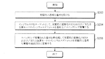
- 実質的に透明な基板を設け、
インジウムスズ(InSn)をターゲットとするスパッタリングによって、実質的に亜酸化のインジウムスズ酸化物(ITO)および/または金属モードのインジウムスズ膜で直接的または間接的に基板を覆い、
前記スパッタリングは、室温または室温に近い温度で行われ、
実質的に亜酸化のITOおよび/または金属モードのインジウムスズ膜を有する前記基板を熱処理して、実質的に亜酸化のITOおよび/または金属モードのインジウムスズ膜の層を実質的に透明で導電性を有する結晶性の合成ITO膜に変換する工程を備えた被覆品の製造方法。 - 基板は、還元鉄ソーダ石灰フロートガラスである請求項1に記載の方法。
- 前記スパッタリング後、実質的に亜酸化のインジウムスズ酸化物(ITO)および/または金属モードのインジウムスズ膜は、アモルファスまたは部分的に結晶質のいずれかである請求項1に記載の方法。
- InSnターゲットは、95/5から80/20までのIn/Sn重量比を有する請求項1に記載の方法。
- 合成ITO膜は、約70オーム/sq.よりも低いシート抵抗を有する請求項1に記載の方法。
- 合成ITO膜は、約50オーム/sq.よりも低いシート抵抗を有する請求項1に記載の方法。
- アモルファスまたは部分的に結晶質のITO膜またはInSn膜を有するガラス基板を少なくとも約600℃の温度で熱による焼き戻しを行うことにより前記熱処理をさらに行う請求項1に記載の方法。
- アモルファスまたは部分的に結晶質のITO膜またはInSn膜を有するガラス基板を約600℃の温度で熱強化することにより前記熱処理をさらに行う請求項1に記載の方法。
- 前記基板および前記実質的に亜酸化のインジウムスズ酸化物(ITO)および/または金属モードのインジウムスズ膜間に緩衝層を配置する工程をさらに備えた請求項1に記載の方法。
- 前記バッファ層は、誘電材料からなる請求項9に記載の方法。
- 前記基板および前記実質的に亜酸化のインジウムスズ酸化物(ITO)および/または金属モードのインジウムスズ膜間に窒化ケイ素からなる層を配置する工程をさらに備えた請求項1に記載の方法。
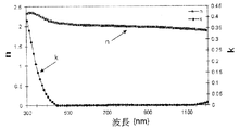
- 合成ITO膜は、少なくとも約70%の可視透過率を有する請求項1に記載の方法。
- 合成ITO膜は、少なくとも約75%の可視透過率を有する請求項1に記載の方法。
- 前記実質的に亜酸化のインジウムスズ酸化物(ITO)層および/または金属モードのインジウムスズ膜は、(InSn)xOyからなり、0<y<0.5、かつx=1−yである請求項1に記載の方法。
- 前記実質的に亜酸化のインジウムスズ酸化物(ITO)層および/または金属モードのインジウムスズ膜は、(InSn)xOyからなり、0.1<y<0.3、かつx=1−yである請求項1に記載の方法。
- 前記スパッタリングを実質的に純アルゴン環境で行う請求項1に記載の方法。
- 前記スパッタリングを0から0.4まで、一層好ましくは0から0.1までの酸素対アルゴン比を有する環境で行う請求項1に記載の方法。
- 実質的に透明なソーダ石灰フロートガラス基板を設け、
インジウムスズ(InSn)をターゲットとするスパッタリングによって、中間膜で直接的または間接的に基板を覆い、
前記中間膜は、実質的に亜酸化のインジウムスズ酸化物(ITO)および/または金属モードのインジウムスズ膜からなり、
前記スパッタリングは、室温または室温に近い温度で行われ、
前記中間膜とともに基板を熱強化するか、または熱による焼き戻しを行って導電性を有する結晶性の合成ITO膜を作り、
前記中間膜は、(InSn)xOyからなり、0<y<0.5、かつx=1−yであり、
前記スパッタリングを0から0.4まで、一層好ましくは0から0.1までの酸素対アルゴン比を有する環境で行う工程を備えた被覆品の製造方法。 - 前記基板および前記中間膜間に誘電体バッファ層を配置する工程をさらに備えた請求項18に記載の方法。
- 合成ITO膜は、誘電体バッファ層とともに少なくとも約70%の可視透過率を有する請求項19に記載の方法。
- ディスプレイパネルを設け、
ITO被膜からなる被覆品を設け、
被覆品は、インジウムスズ(InSn)をターゲットとするスパッタリングによって直接的または間接的に基板を覆う中間膜を有し、
前記中間膜は、実質的に亜酸化のインジウムスズ酸化物(ITO)および/または金属モードのインジウムスズ膜からなり、
前記スパッタリングは、室温または室温に近い温度で行われ、
基板および中間膜を熱処理して導電性を有する結晶性の合成ITO膜を作り、
前記中間膜は、(InSn)xOyからなり、0<y<0.5、かつx=1−yであり、
前記スパッタリングを0から0.4まで、一層好ましくは0から0.1までの酸素対アルゴン比を有する環境で行う工程を備えたタッチパネルディスプレイ装置の製造方法。
Applications Claiming Priority (3)
| Application Number | Priority Date | Filing Date | Title |
|---|---|---|---|
| US12/292,406 | 2008-11-18 | ||
| US12/292,406 US8080141B2 (en) | 2008-11-18 | 2008-11-18 | ITO-coated article and/or method of making the same via heat treating |
| PCT/US2009/060416 WO2010059311A1 (en) | 2008-11-18 | 2009-10-13 | Ito-coated article for use with touch panel display assemblies, and/or method of making the same |
Publications (1)
| Publication Number | Publication Date |
|---|---|
| JP2012509397A true JP2012509397A (ja) | 2012-04-19 |
Family
ID=41478945
Family Applications (1)
| Application Number | Title | Priority Date | Filing Date |
|---|---|---|---|
| JP2011536361A Pending JP2012509397A (ja) | 2008-11-18 | 2009-10-13 | タッチパネルディスプレイとともに使用するためのito被覆品の製造方法、および/または前記ito被覆品の製造方法 |
Country Status (7)
| Country | Link |
|---|---|
| US (3) | US8080141B2 (ja) |
| EP (1) | EP2370611A1 (ja) |
| JP (1) | JP2012509397A (ja) |
| KR (1) | KR20110098706A (ja) |
| BR (1) | BRPI0921775A2 (ja) |
| TW (1) | TW201022458A (ja) |
| WO (1) | WO2010059311A1 (ja) |
Cited By (1)
| Publication number | Priority date | Publication date | Assignee | Title |
|---|---|---|---|---|
| JP2015074788A (ja) * | 2013-10-07 | 2015-04-20 | 三菱マテリアル株式会社 | Inスパッタリングターゲット及びIn膜 |
Families Citing this family (30)
| Publication number | Priority date | Publication date | Assignee | Title |
|---|---|---|---|---|
| US8080141B2 (en) | 2008-11-18 | 2011-12-20 | Guardian Industries Corp. | ITO-coated article and/or method of making the same via heat treating |
| US8236118B2 (en) | 2009-08-07 | 2012-08-07 | Guardian Industries Corp. | Debonding and transfer techniques for hetero-epitaxially grown graphene, and products including the same |
| US10060180B2 (en) | 2010-01-16 | 2018-08-28 | Cardinal Cg Company | Flash-treated indium tin oxide coatings, production methods, and insulating glass unit transparent conductive coating technology |
| US10000411B2 (en) | 2010-01-16 | 2018-06-19 | Cardinal Cg Company | Insulating glass unit transparent conductivity and low emissivity coating technology |
| US10000965B2 (en) | 2010-01-16 | 2018-06-19 | Cardinal Cg Company | Insulating glass unit transparent conductive coating technology |
| US8658262B2 (en) | 2010-01-16 | 2014-02-25 | Cardinal Cg Company | High quality emission control coatings, emission control glazings, and production methods |
| KR101298837B1 (ko) * | 2010-06-25 | 2013-08-23 | 주식회사 유아이디 | 터치 패널용 ito 코팅 유리 제조 방법 및 이에 사용되는 스퍼터링 장치 |
| KR101167418B1 (ko) * | 2010-09-20 | 2012-07-19 | 삼성전기주식회사 | 저항막식 터치스크린 |
| US20130019934A1 (en) * | 2011-07-22 | 2013-01-24 | Primestar Solar, Inc. | Oxygen getter layer for photovoltaic devices and methods of their manufacture |
| WO2013125191A1 (ja) * | 2012-02-24 | 2013-08-29 | パナソニック株式会社 | 入力装置 |
| US8524526B1 (en) * | 2012-08-14 | 2013-09-03 | Guardian Industries Corp. | Organic light emitting diode with transparent electrode and method of making same |
| US8766245B2 (en) | 2012-08-14 | 2014-07-01 | Guardian Industries Corp. | Organic light emitting diode with transparent electrode and method of making same |
| US9354755B2 (en) | 2012-11-27 | 2016-05-31 | Guardian Industries Corp. | Projected capacitive touch panel with a silver-inclusive transparent conducting layer(s) |
| US10248274B2 (en) | 2012-11-27 | 2019-04-02 | Guardian Glass, LLC | Transparent conductive coating for capacitive touch panel and method of making same |
| US9557871B2 (en) | 2015-04-08 | 2017-01-31 | Guardian Industries Corp. | Transparent conductive coating for capacitive touch panel or the like |
| US10222921B2 (en) | 2012-11-27 | 2019-03-05 | Guardian Glass, LLC | Transparent conductive coating for capacitive touch panel with silver having increased resistivity |
| US9733779B2 (en) | 2012-11-27 | 2017-08-15 | Guardian Industries Corp. | Projected capacitive touch panel with silver-inclusive transparent conducting layer(s), and/or method of making the same |
| US10216347B2 (en) | 2012-11-27 | 2019-02-26 | Guardian Glass, LLC | Transparent conductive coating for capacitive touch panel with silver having adjusted resistance |
| JP5672338B2 (ja) * | 2013-06-04 | 2015-02-18 | Smk株式会社 | タッチパネルおよびタッチパネルの製造方法 |
| US9988707B2 (en) | 2014-05-30 | 2018-06-05 | Ppg Industries Ohio, Inc. | Transparent conducting indium doped tin oxide |
| US10133108B2 (en) | 2015-04-08 | 2018-11-20 | Guardian Glass, LLC | Vending machines with large area transparent touch electrode technology, and/or associated methods |
| US10145005B2 (en) | 2015-08-19 | 2018-12-04 | Guardian Glass, LLC | Techniques for low temperature direct graphene growth on glass |
| KR102513362B1 (ko) * | 2015-12-11 | 2023-03-24 | 삼성디스플레이 주식회사 | 액정 표시 패널 및 이의 제조 방법 |
| WO2017196034A1 (ko) * | 2016-05-09 | 2017-11-16 | 주식회사 엘지화학 | 도전성 투광 필름 |
| KR102159491B1 (ko) | 2016-05-09 | 2020-09-24 | 주식회사 엘지화학 | 도전성 투광 필름 |
| KR20190085487A (ko) * | 2018-01-10 | 2019-07-18 | 어플라이드 머티어리얼스, 인코포레이티드 | Euv 리소그래피용 pvd 막들 |
| US10539864B2 (en) | 2018-02-08 | 2020-01-21 | Guardian Glass, LLC | Capacitive touch panel having diffuser and patterned electrode |
| US11028012B2 (en) | 2018-10-31 | 2021-06-08 | Cardinal Cg Company | Low solar heat gain coatings, laminated glass assemblies, and methods of producing same |
| FR3088850B1 (fr) * | 2018-11-28 | 2020-12-11 | Saint Gobain | Procede de fabrication d’un vitrage electrochrome |
| CN114436538B (zh) * | 2021-12-20 | 2023-05-30 | 凯盛信息显示材料(洛阳)有限公司 | 高透过消影导电玻璃及其制造方法 |
Citations (5)
| Publication number | Priority date | Publication date | Assignee | Title |
|---|---|---|---|---|
| JPS59116138A (ja) * | 1982-11-03 | 1984-07-04 | ドネリ−・ミラ−ズ・インコ−ポレイテツド | 湾曲、導電性被覆したガラス部材を製造する方法およびその製品 |
| JPS6212010A (ja) * | 1985-07-09 | 1987-01-21 | 富士通株式会社 | 透光性導電体膜の形成方法 |
| JPH09226046A (ja) * | 1996-02-22 | 1997-09-02 | Mitsui Toatsu Chem Inc | 透明導電性積層体及びその製造方法 |
| JP2004149400A (ja) * | 2002-09-02 | 2004-05-27 | Asahi Glass Co Ltd | 断熱ガラスとその製造方法 |
| JP2007311040A (ja) * | 2006-05-16 | 2007-11-29 | Bridgestone Corp | 結晶性ito薄膜の成膜方法、結晶性ito薄膜及びフィルム、並びに抵抗膜式タッチパネル |
Family Cites Families (19)
| Publication number | Priority date | Publication date | Assignee | Title |
|---|---|---|---|---|
| FR2633920B1 (fr) * | 1988-07-08 | 1992-02-21 | Saint Gobain Vitrage | Procede pour produire une couche transparente a faible resistivite |
| US5650597A (en) | 1995-01-20 | 1997-07-22 | Dynapro Systems, Inc. | Capacitive touch sensor |
| US6123415A (en) * | 1995-12-21 | 2000-09-26 | Kabushiki Kaisha Toshiba | Ink jet recording apparatus |
| CA2239721A1 (en) * | 1996-01-26 | 1997-07-31 | Tetra Laval Holdings & Finance S.A. | Method and apparatus for printing images on packaging material |
| GB9626696D0 (en) * | 1996-12-23 | 1997-02-12 | Ishida Seisakusho | Method of printing film at form-fill-seal packaging machine form-fill-seal packaging machine using the method |
| US6057903A (en) | 1998-08-18 | 2000-05-02 | International Business Machines Corporation | Liquid crystal display device employing a guard plane between a layer for measuring touch position and common electrode layer |
| US6204897B1 (en) | 1998-08-18 | 2001-03-20 | International Business Machines Corporation | Integrated resistor for measuring touch position in a liquid crystal display device |
| DE19913855A1 (de) * | 1999-03-26 | 2000-09-28 | Focke & Co | Verfahren und Vorrichtung zum Bedrucken von Zuschnitten |
| JP2001315321A (ja) * | 2000-05-11 | 2001-11-13 | Fuji Photo Film Co Ltd | インクジェット式印刷方法及び印刷装置 |
| EP1188551B1 (en) | 2000-09-14 | 2006-08-09 | Asahi Glass Co., Ltd. | Laminated glass |
| US6743488B2 (en) * | 2001-05-09 | 2004-06-01 | Cpfilms Inc. | Transparent conductive stratiform coating of indium tin oxide |
| DE10228523B4 (de) | 2001-11-14 | 2017-09-21 | Lg Display Co., Ltd. | Berührungstablett |
| US6550905B1 (en) * | 2001-11-19 | 2003-04-22 | Dotrix N.V. | Radiation curable inkjet ink relatively free of photoinitiator and method and apparatus of curing the ink |
| WO2003075207A2 (en) | 2002-03-01 | 2003-09-12 | Planar Systems, Inc. | Reflection resistant touch screens |
| KR100480823B1 (ko) | 2002-11-14 | 2005-04-07 | 엘지.필립스 엘시디 주식회사 | 표시장치용 터치 패널 |
| JPWO2006061964A1 (ja) * | 2004-12-08 | 2008-06-05 | 旭硝子株式会社 | 導電膜付き基体およびその製造方法 |
| JPWO2007029457A1 (ja) | 2005-09-02 | 2009-03-12 | 出光興産株式会社 | 導電性組成物膜、電子注入電極及び有機エレクトロルミネッセンス素子 |
| TWI325639B (en) * | 2007-03-15 | 2010-06-01 | Au Optronics Corp | Semiconductor structure and fabricating method thereof for liquid crystal display device |
| US8080141B2 (en) | 2008-11-18 | 2011-12-20 | Guardian Industries Corp. | ITO-coated article and/or method of making the same via heat treating |
-
2008
- 2008-11-18 US US12/292,406 patent/US8080141B2/en not_active Expired - Fee Related
-
2009
- 2009-10-13 KR KR1020117003074A patent/KR20110098706A/ko not_active Withdrawn
- 2009-10-13 WO PCT/US2009/060416 patent/WO2010059311A1/en not_active Ceased
- 2009-10-13 JP JP2011536361A patent/JP2012509397A/ja active Pending
- 2009-10-13 EP EP09740586A patent/EP2370611A1/en not_active Withdrawn
- 2009-10-13 BR BRPI0921775A patent/BRPI0921775A2/pt not_active IP Right Cessation
- 2009-10-22 TW TW098135765A patent/TW201022458A/zh unknown
-
2011
- 2011-11-22 US US13/302,052 patent/US8313620B2/en not_active Expired - Fee Related
-
2012
- 2012-11-05 US US13/668,732 patent/US8518221B2/en not_active Expired - Fee Related
Patent Citations (5)
| Publication number | Priority date | Publication date | Assignee | Title |
|---|---|---|---|---|
| JPS59116138A (ja) * | 1982-11-03 | 1984-07-04 | ドネリ−・ミラ−ズ・インコ−ポレイテツド | 湾曲、導電性被覆したガラス部材を製造する方法およびその製品 |
| JPS6212010A (ja) * | 1985-07-09 | 1987-01-21 | 富士通株式会社 | 透光性導電体膜の形成方法 |
| JPH09226046A (ja) * | 1996-02-22 | 1997-09-02 | Mitsui Toatsu Chem Inc | 透明導電性積層体及びその製造方法 |
| JP2004149400A (ja) * | 2002-09-02 | 2004-05-27 | Asahi Glass Co Ltd | 断熱ガラスとその製造方法 |
| JP2007311040A (ja) * | 2006-05-16 | 2007-11-29 | Bridgestone Corp | 結晶性ito薄膜の成膜方法、結晶性ito薄膜及びフィルム、並びに抵抗膜式タッチパネル |
Non-Patent Citations (1)
| Title |
|---|
| JPN5012003483; CHAUDHURI S: 'MICROSTRUCTURE OF INDIUM TIN OXIDE FILMS PRODUCED BY THE D.C. SPUTTERING TECHNIQUE' THIN SOLID FILMS V148 N3, 19870427, P279-284, ELSEVIER-SEQUOIA S.A. * |
Cited By (1)
| Publication number | Priority date | Publication date | Assignee | Title |
|---|---|---|---|---|
| JP2015074788A (ja) * | 2013-10-07 | 2015-04-20 | 三菱マテリアル株式会社 | Inスパッタリングターゲット及びIn膜 |
Also Published As
| Publication number | Publication date |
|---|---|
| WO2010059311A1 (en) | 2010-05-27 |
| BRPI0921775A2 (pt) | 2016-01-12 |
| US20120064234A1 (en) | 2012-03-15 |
| KR20110098706A (ko) | 2011-09-01 |
| EP2370611A1 (en) | 2011-10-05 |
| US8080141B2 (en) | 2011-12-20 |
| TW201022458A (en) | 2010-06-16 |
| US20130059065A1 (en) | 2013-03-07 |
| US8313620B2 (en) | 2012-11-20 |
| US8518221B2 (en) | 2013-08-27 |
| US20100122900A1 (en) | 2010-05-20 |
Similar Documents
| Publication | Publication Date | Title |
|---|---|---|
| JP2012509397A (ja) | タッチパネルディスプレイとともに使用するためのito被覆品の製造方法、および/または前記ito被覆品の製造方法 | |
| JP6328122B2 (ja) | 低い可視光線透過率を有する低放射率被覆製品 | |
| EP2024293B1 (en) | Method of making thermally tempered coated article with transparent conductive oxide (tco) coating in color compression configuration, and product made using same | |
| US7597964B2 (en) | Thermally tempered coated article with transparent conductive oxide (TCO) coating | |
| JPH02217339A (ja) | 透明導電ガラス | |
| KR20170077217A (ko) | 반사 방지 코팅된 유리 제품 | |
| CN103561951A (zh) | 低辐射率层叠体及多层玻璃 | |
| CN102194539A (zh) | 透明导电叠层体及其制造方法 | |
| EP2148240B1 (en) | Transparent electrode | |
| CN104603320B (zh) | 带透明电极的基板的制造方法、以及带透明电极的基板 | |
| JPH08111123A (ja) | 透明導電膜とその製造方法およびスパッタリングターゲット | |
| KR101768286B1 (ko) | 전도성 구조체 전구체, 전도성 구조체 및 이의 제조방법 | |
| KR102791294B1 (ko) | 투명 도전성 필름 | |
| WO2021001691A4 (ja) | 透明導電性フィルム | |
| CN106165025A (zh) | 层叠体、导电性层叠体及电子设备 | |
| JP2001210144A (ja) | 透明導電膜付き基板とその製造方法 | |
| JP2005190700A (ja) | 透明導電膜付き基板とその製造方法 | |
| JP3630374B2 (ja) | 透明導電膜付ガラス及び透明導電膜の成膜方法 | |
| WO2026068931A1 (en) | Coated substrate | |
| JPH07291664A (ja) | 透明導電性薄膜 | |
| CN114127864A (zh) | 透明导电性薄膜 | |
| JPH06320661A (ja) | 透明導電膜の製造方法 |
Legal Events
| Date | Code | Title | Description |
|---|---|---|---|
| A621 | Written request for application examination |
Free format text: JAPANESE INTERMEDIATE CODE: A621 Effective date: 20120919 |
|
| A977 | Report on retrieval |
Free format text: JAPANESE INTERMEDIATE CODE: A971007 Effective date: 20131010 |
|
| A131 | Notification of reasons for refusal |
Free format text: JAPANESE INTERMEDIATE CODE: A131 Effective date: 20131022 |
|
| A601 | Written request for extension of time |
Free format text: JAPANESE INTERMEDIATE CODE: A601 Effective date: 20140116 |
|
| A602 | Written permission of extension of time |
Free format text: JAPANESE INTERMEDIATE CODE: A602 Effective date: 20140123 |
|
| A02 | Decision of refusal |
Free format text: JAPANESE INTERMEDIATE CODE: A02 Effective date: 20150106 |