JP2012509403A - ZnOクバン混合物を含む調製物、及び前記調製物を用いるZnO半導体層製造方法 - Google Patents
ZnOクバン混合物を含む調製物、及び前記調製物を用いるZnO半導体層製造方法 Download PDFInfo
- Publication number
- JP2012509403A JP2012509403A JP2011536814A JP2011536814A JP2012509403A JP 2012509403 A JP2012509403 A JP 2012509403A JP 2011536814 A JP2011536814 A JP 2011536814A JP 2011536814 A JP2011536814 A JP 2011536814A JP 2012509403 A JP2012509403 A JP 2012509403A
- Authority
- JP
- Japan
- Prior art keywords
- zno
- preparation
- cubane
- och
- weight
- Prior art date
- Legal status (The legal status is an assumption and is not a legal conclusion. Google has not performed a legal analysis and makes no representation as to the accuracy of the status listed.)
- Granted
Links
Images



Classifications
-
- C—CHEMISTRY; METALLURGY
- C23—COATING METALLIC MATERIAL; COATING MATERIAL WITH METALLIC MATERIAL; CHEMICAL SURFACE TREATMENT; DIFFUSION TREATMENT OF METALLIC MATERIAL; COATING BY VACUUM EVAPORATION, BY SPUTTERING, BY ION IMPLANTATION OR BY CHEMICAL VAPOUR DEPOSITION, IN GENERAL; INHIBITING CORROSION OF METALLIC MATERIAL OR INCRUSTATION IN GENERAL
- C23C—COATING METALLIC MATERIAL; COATING MATERIAL WITH METALLIC MATERIAL; SURFACE TREATMENT OF METALLIC MATERIAL BY DIFFUSION INTO THE SURFACE, BY CHEMICAL CONVERSION OR SUBSTITUTION; COATING BY VACUUM EVAPORATION, BY SPUTTERING, BY ION IMPLANTATION OR BY CHEMICAL VAPOUR DEPOSITION, IN GENERAL
- C23C18/00—Chemical coating by decomposition of either liquid compounds or solutions of the coating forming compounds, without leaving reaction products of surface material in the coating; Contact plating
- C23C18/02—Chemical coating by decomposition of either liquid compounds or solutions of the coating forming compounds, without leaving reaction products of surface material in the coating; Contact plating by thermal decomposition
- C23C18/12—Chemical coating by decomposition of either liquid compounds or solutions of the coating forming compounds, without leaving reaction products of surface material in the coating; Contact plating by thermal decomposition characterised by the deposition of inorganic material other than metallic material
- C23C18/1204—Chemical coating by decomposition of either liquid compounds or solutions of the coating forming compounds, without leaving reaction products of surface material in the coating; Contact plating by thermal decomposition characterised by the deposition of inorganic material other than metallic material inorganic material, e.g. non-oxide and non-metallic such as sulfides, nitrides based compounds
- C23C18/1208—Oxides, e.g. ceramics
- C23C18/1216—Metal oxides
-
- C—CHEMISTRY; METALLURGY
- C23—COATING METALLIC MATERIAL; COATING MATERIAL WITH METALLIC MATERIAL; CHEMICAL SURFACE TREATMENT; DIFFUSION TREATMENT OF METALLIC MATERIAL; COATING BY VACUUM EVAPORATION, BY SPUTTERING, BY ION IMPLANTATION OR BY CHEMICAL VAPOUR DEPOSITION, IN GENERAL; INHIBITING CORROSION OF METALLIC MATERIAL OR INCRUSTATION IN GENERAL
- C23C—COATING METALLIC MATERIAL; COATING MATERIAL WITH METALLIC MATERIAL; SURFACE TREATMENT OF METALLIC MATERIAL BY DIFFUSION INTO THE SURFACE, BY CHEMICAL CONVERSION OR SUBSTITUTION; COATING BY VACUUM EVAPORATION, BY SPUTTERING, BY ION IMPLANTATION OR BY CHEMICAL VAPOUR DEPOSITION, IN GENERAL
- C23C16/00—Chemical coating by decomposition of gaseous compounds, without leaving reaction products of surface material in the coating, i.e. chemical vapour deposition [CVD] processes
- C23C16/06—Chemical coating by decomposition of gaseous compounds, without leaving reaction products of surface material in the coating, i.e. chemical vapour deposition [CVD] processes characterised by the deposition of metallic material
-
- C—CHEMISTRY; METALLURGY
- C23—COATING METALLIC MATERIAL; COATING MATERIAL WITH METALLIC MATERIAL; CHEMICAL SURFACE TREATMENT; DIFFUSION TREATMENT OF METALLIC MATERIAL; COATING BY VACUUM EVAPORATION, BY SPUTTERING, BY ION IMPLANTATION OR BY CHEMICAL VAPOUR DEPOSITION, IN GENERAL; INHIBITING CORROSION OF METALLIC MATERIAL OR INCRUSTATION IN GENERAL
- C23C—COATING METALLIC MATERIAL; COATING MATERIAL WITH METALLIC MATERIAL; SURFACE TREATMENT OF METALLIC MATERIAL BY DIFFUSION INTO THE SURFACE, BY CHEMICAL CONVERSION OR SUBSTITUTION; COATING BY VACUUM EVAPORATION, BY SPUTTERING, BY ION IMPLANTATION OR BY CHEMICAL VAPOUR DEPOSITION, IN GENERAL
- C23C18/00—Chemical coating by decomposition of either liquid compounds or solutions of the coating forming compounds, without leaving reaction products of surface material in the coating; Contact plating
- C23C18/02—Chemical coating by decomposition of either liquid compounds or solutions of the coating forming compounds, without leaving reaction products of surface material in the coating; Contact plating by thermal decomposition
- C23C18/12—Chemical coating by decomposition of either liquid compounds or solutions of the coating forming compounds, without leaving reaction products of surface material in the coating; Contact plating by thermal decomposition characterised by the deposition of inorganic material other than metallic material
- C23C18/1204—Chemical coating by decomposition of either liquid compounds or solutions of the coating forming compounds, without leaving reaction products of surface material in the coating; Contact plating by thermal decomposition characterised by the deposition of inorganic material other than metallic material inorganic material, e.g. non-oxide and non-metallic such as sulfides, nitrides based compounds
- C23C18/122—Inorganic polymers, e.g. silanes, polysilazanes, polysiloxanes
-
- C—CHEMISTRY; METALLURGY
- C23—COATING METALLIC MATERIAL; COATING MATERIAL WITH METALLIC MATERIAL; CHEMICAL SURFACE TREATMENT; DIFFUSION TREATMENT OF METALLIC MATERIAL; COATING BY VACUUM EVAPORATION, BY SPUTTERING, BY ION IMPLANTATION OR BY CHEMICAL VAPOUR DEPOSITION, IN GENERAL; INHIBITING CORROSION OF METALLIC MATERIAL OR INCRUSTATION IN GENERAL
- C23C—COATING METALLIC MATERIAL; COATING MATERIAL WITH METALLIC MATERIAL; SURFACE TREATMENT OF METALLIC MATERIAL BY DIFFUSION INTO THE SURFACE, BY CHEMICAL CONVERSION OR SUBSTITUTION; COATING BY VACUUM EVAPORATION, BY SPUTTERING, BY ION IMPLANTATION OR BY CHEMICAL VAPOUR DEPOSITION, IN GENERAL
- C23C18/00—Chemical coating by decomposition of either liquid compounds or solutions of the coating forming compounds, without leaving reaction products of surface material in the coating; Contact plating
- C23C18/02—Chemical coating by decomposition of either liquid compounds or solutions of the coating forming compounds, without leaving reaction products of surface material in the coating; Contact plating by thermal decomposition
- C23C18/12—Chemical coating by decomposition of either liquid compounds or solutions of the coating forming compounds, without leaving reaction products of surface material in the coating; Contact plating by thermal decomposition characterised by the deposition of inorganic material other than metallic material
- C23C18/1229—Composition of the substrate
- C23C18/1233—Organic substrates
-
- C—CHEMISTRY; METALLURGY
- C23—COATING METALLIC MATERIAL; COATING MATERIAL WITH METALLIC MATERIAL; CHEMICAL SURFACE TREATMENT; DIFFUSION TREATMENT OF METALLIC MATERIAL; COATING BY VACUUM EVAPORATION, BY SPUTTERING, BY ION IMPLANTATION OR BY CHEMICAL VAPOUR DEPOSITION, IN GENERAL; INHIBITING CORROSION OF METALLIC MATERIAL OR INCRUSTATION IN GENERAL
- C23C—COATING METALLIC MATERIAL; COATING MATERIAL WITH METALLIC MATERIAL; SURFACE TREATMENT OF METALLIC MATERIAL BY DIFFUSION INTO THE SURFACE, BY CHEMICAL CONVERSION OR SUBSTITUTION; COATING BY VACUUM EVAPORATION, BY SPUTTERING, BY ION IMPLANTATION OR BY CHEMICAL VAPOUR DEPOSITION, IN GENERAL
- C23C18/00—Chemical coating by decomposition of either liquid compounds or solutions of the coating forming compounds, without leaving reaction products of surface material in the coating; Contact plating
- C23C18/02—Chemical coating by decomposition of either liquid compounds or solutions of the coating forming compounds, without leaving reaction products of surface material in the coating; Contact plating by thermal decomposition
- C23C18/12—Chemical coating by decomposition of either liquid compounds or solutions of the coating forming compounds, without leaving reaction products of surface material in the coating; Contact plating by thermal decomposition characterised by the deposition of inorganic material other than metallic material
- C23C18/1229—Composition of the substrate
- C23C18/1245—Inorganic substrates other than metallic
-
- C—CHEMISTRY; METALLURGY
- C23—COATING METALLIC MATERIAL; COATING MATERIAL WITH METALLIC MATERIAL; CHEMICAL SURFACE TREATMENT; DIFFUSION TREATMENT OF METALLIC MATERIAL; COATING BY VACUUM EVAPORATION, BY SPUTTERING, BY ION IMPLANTATION OR BY CHEMICAL VAPOUR DEPOSITION, IN GENERAL; INHIBITING CORROSION OF METALLIC MATERIAL OR INCRUSTATION IN GENERAL
- C23C—COATING METALLIC MATERIAL; COATING MATERIAL WITH METALLIC MATERIAL; SURFACE TREATMENT OF METALLIC MATERIAL BY DIFFUSION INTO THE SURFACE, BY CHEMICAL CONVERSION OR SUBSTITUTION; COATING BY VACUUM EVAPORATION, BY SPUTTERING, BY ION IMPLANTATION OR BY CHEMICAL VAPOUR DEPOSITION, IN GENERAL
- C23C18/00—Chemical coating by decomposition of either liquid compounds or solutions of the coating forming compounds, without leaving reaction products of surface material in the coating; Contact plating
- C23C18/02—Chemical coating by decomposition of either liquid compounds or solutions of the coating forming compounds, without leaving reaction products of surface material in the coating; Contact plating by thermal decomposition
- C23C18/12—Chemical coating by decomposition of either liquid compounds or solutions of the coating forming compounds, without leaving reaction products of surface material in the coating; Contact plating by thermal decomposition characterised by the deposition of inorganic material other than metallic material
- C23C18/125—Process of deposition of the inorganic material
- C23C18/1295—Process of deposition of the inorganic material with after-treatment of the deposited inorganic material
Landscapes
- Chemical & Material Sciences (AREA)
- Engineering & Computer Science (AREA)
- Mechanical Engineering (AREA)
- Metallurgy (AREA)
- General Chemical & Material Sciences (AREA)
- Chemical Kinetics & Catalysis (AREA)
- Organic Chemistry (AREA)
- Materials Engineering (AREA)
- Physics & Mathematics (AREA)
- Inorganic Chemistry (AREA)
- Thermal Sciences (AREA)
- Ceramic Engineering (AREA)
- Liquid Deposition Of Substances Of Which Semiconductor Devices Are Composed (AREA)
- Inorganic Compounds Of Heavy Metals (AREA)
- Chemically Coating (AREA)
- Thin Film Transistor (AREA)
- Inks, Pencil-Leads, Or Crayons (AREA)
- Organic Low-Molecular-Weight Compounds And Preparation Thereof (AREA)
Abstract
Description
a)以下の少なくとも2つの異なるZnOクバン、
i)SATP条件で固体の少なくとも1つのZnOクバン(SATP=標準雰囲気温度及び圧力;25℃及び105Pa)
ii)SATP条件で液体の少なくとも1つのZnOクバン、並びに
b)少なくとも1つの溶剤
を含む調製物によって解決される。

R1=8〜13個の炭素原子を有する直鎖状、又は分枝鎖状、又は脂環式の基、
R2=水素、1〜8個のC原子をそれぞれ有する、アシル基、アルキル基、又はカルボン酸基、
SO=スチレンオキシド、EO=エチレンオキシド、PO=プロピレンオキシド、
BO=ブチレンオキシド、
a=1〜5、
b=3〜50、
c=0〜3、
d=0〜3、ここでb≧a+c+dである]
の、ランダムな分布を有する、又はブロックコポリマーとしてのスチレンオキシドベースのポリアルキレンオキシド。
ただしR=
前記式中、
x=1又は2、
n=2〜18
m、o=2〜100、
k=2〜4
R’’=H、又は線状又は分枝状のアルキル基、このアルキル基は場合により、付加的な官能基で置換されていてよく、
R’=アルキル基、アルカリール基、アルケニル基、又はスルホプロピル基である。
R1=1〜22個の炭素原子を有する直鎖状、分枝状、又は脂環式基、
SO=スチレンオキシド、EO=エチレンオキシド、BO=ブチレンオキシド、
a=1〜<2、
b=0〜100、
c=0〜10、
d=0〜3、ここでb≧a+c+dである]
のブロックコポリマー及びその塩を使用することができる。
A)1つ又は複数のアミノ官能性ポリマーと、
B)一般式(4)/(4a)
C)一般式(5)/(5a)
前記式中、
Tは水素基、及び/又は場合により置換された、1〜24個の炭素原子を有する線状、又は分枝状のアリール基、アリールアルキル基、アルキル基、又はアルケニル基であり、
Aは、線状、分枝状、環状、及び芳香族の炭化水素基の群から選択される少なくとも1つの二価の基であり、
Zは、スルホン酸、硫酸、ホスホン酸、リン酸、カルボン酸、イソシアネート、エポキシドの群から、とりわけリン酸及び(メタ)アクリル酸の群から選択される少なくとも1つの基であり、
Bは一般式(6)
dは0以上、好適には1〜5であり、
l、m、nは相互に独立して2以上、好適には2〜4であり、
x、yは相互に独立して2以上である。
式中、
R1は1〜4個の炭素原子を有するアルキル基、又はアリール基であるが、基R1のうち少なくとも80%がメチル基である
R2は分子中で同じでも異なっていてもよく、以下の意味を有することができる:
a)
R3は水素基、又はアルキル基であり、
R4は水素基、アルキル基、又はカルボキシ基であり、
cは1〜20の数であり、
dは0〜50の数であり、
eは0〜50の数である、
又は
b)
R5は、水素基、アルキル基、カルボキシル基、又は場合によりエーテル基含有ジメチロールプロパン基であり、
fは、2〜20の数である、
又は
c)
R6は、水素基、アルキル基、又はカルボキシル基であり、
gは、2〜6の数であり、
hは、0〜20の数であり、
iは、1〜50の数であり、
jは、0〜10の数であり、
kは、0〜10の数である、
又は
d)基R1に相当するもの、但し、平均分子で少なくとも1個の基R2が、(a)の意味を有し、この場合aは、1〜500、好適には1〜200、とりわけ1〜50の数であり、bは、0〜10の数、特に5未満、とりわけ0である。
a)式(8a)、(8b)、(8c)、及び/又は(8d)
前記式中、
R1=H、1〜5個のC原子を有する脂肪族炭化水素基、
p=1〜4、q=0〜6、t=0〜4、i=1〜6、l=1〜2、m=2〜18であり、
ここでH原子の添え字は、l×mの積により得られ、n=0〜100、o=0〜100、SO=スチレンオキシドであり、
ここで(SO)i及びアルキレンオキシド誘導体はランダムに又はブロック状にポリエーテル中で分布していてよいが、これらの基は好適にはブロック状に構成されており、以下の
前記式中、R2は、H、1〜20個のC原子を有する脂肪族の、場合により分枝状の炭化水素基、5〜8個のC原子を有する脂環式炭化水素基、6〜14個のC原子を有するアリール基であり、この基は、場合により置換されているか、又はリン酸エステル誘導体(好適にはモノエステル)、スルフェート誘導体、又はスルホネート誘導体であってよく、
b)式(9)
前記式中、
Sは、−H、−COOMa、−COOR3を表わし、
Mは、水素、一価又は二価の金属カチオン、アンモニウムイオン、有機アミン基を表わし、
aは1、又はMが二価の金属カチオンの場合には1/2であり、
R3は、1〜20個のC原子を有する脂肪族の、場合により分枝状の炭化水素基、5〜8個のC原子を有する脂環式炭化水素基、6〜14個のC原子を有するアリール基であり、
Tは、−U1−R4、又は−U1−(CmHlmO)n−(CmHlmO)o−R2であり、
U1は、−COO−、−CONH−、−CONR3−、−O−、−CH2O−であり、
R4は、H、Ma、R3、又は−Q1−NQ2Q3であり、
ここでQ1は、2〜24個の炭素原子を有する二価のアルキレン基であり、
Q2及びQ3は、1〜12個の炭素原子を有する脂肪族及び/又は脂環式アルキル基であり、場合によっては
c)式(10)
前記式中、
T1は、−U1−(CmHlmO)n−(CmHlmO)o−R5であり、
R5はR4、又は
ここでU2は−OOC−、−NHOC−、−O−、−O−CH2であり、
ここでm、n、l、o、S、R1、R2、及びU1は上記の意味を有する。
実施例1:
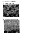
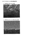
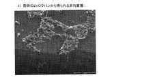
トルエン2mL中の、SATP条件で液体のZnOクバン([MeZn(OCH2CH2OCH3)]4、400mg)、及びSATP条件で固体のZnOクバン([MeZn(O−t−Bu)4、400mg])の50/50質量%の混合物を、スピンコート(2000rpm、30秒)でSi/SiO2基板上に施与し、400℃で乾燥炉で加熱した。
トルエン2mL中の、SATP条件で液体のZnOクバン([MeZn(OCH2CH2OCH3)]4、400mg)、及びSATP条件で固体のZnOクバン([MeZn(O−t−Bu)4、400mg])の50/50質量%の混合物を、スピンコート(2000rpm、30秒)でSi/SiO2基板上に施与し、300℃で乾燥炉で加熱した。
トルエン2mL中の、SATP条件で液体のZnOクバン([MeZn(OCH2CH2OCH3)]4、400mg)、及びSATP条件で固体のZnOクバン([MeZn(O−t−Bu)4、400mg])の50/50質量%の混合物を、スピンコート(2000rpm、30秒)でSi/SiO2基板上に施与し、200℃で乾燥炉で加熱した。
Claims (21)
- a)以下の少なくとも2つの異なるZnOクバン
i)SATP条件で固体の少なくとも1つのZnOクバン、及び
ii)SATP条件で液体の少なくとも1つのZnOクバン、並びに、
b)少なくとも1つの溶剤
を含む調製物。 - SATP条件で固体の前記ZnOクバンが、105Paで120〜300℃、特に好ましくは150〜250℃の分解点を有することを特徴とする、請求項1に記載の調製物。
- SATP条件で固体の前記ZnOクバンが、一般式
[R1Zn(OR2)]4
[式中、R1=Me又はEtであり、R2=t−Bu又はi−Prである]
のZnOクバンであることを特徴とする、請求項1又は2に記載の調製物。 - SATP条件で固体の前記ZnOクバンが、[MeZn(O−t−Bu)]4、又は[MeZn(O−i−Pr)]4であることを特徴とする、請求項3に記載の調製物。
- SATP条件で液体の前記ZnOクバンが、常圧で25〜−100℃、特に好ましくは0〜−30℃の融点を有することを特徴とする、請求項1から4までのいずれか1項に記載の調製物。
- SATP条件で液体の前記ZnOクバンが、一般式
[R1Zn(OR2)]4
[式中、R1=Me又はEtであり、R2=CH2CH2OCH3、CH2CH2OCH2CH3、CH2OCH2CH3、CH2OCH3、又はCH2CH2CH2OCH3である]
ことを特徴とする、請求項1から5までのいずれか1項に記載の調製物。 - SATP条件で液体の前記ZnOクバンが、[MeZn(OCH2CH2OCH3)]4であることを特徴とする、請求項6に記載の調製物。
- 常圧で固体の少なくとも1つのZnOクバンが、固体及び液体のZnOクバンの全質量に対して10〜90質量%、好ましくは30〜70質量%、極めて特に好ましくは40〜60質量%の割合で存在することを特徴とする、請求項1から7までのいずれか1項に記載の調製物。
- 少なくとも1つの溶剤が、非プロトン性溶剤の群、特に好ましくはトルエン、キシレン、アニソール、メシチレン、n−ヘキサン、n−ヘプタン、トリス−(3,6−ジオキサヘプチル)−アミン(TDA)、2−アミノメチルテトラヒドロフラン、フェネトール、4−メチルアニソール、3−メチルアニソール、メチルベンゾエート、N−メチル−2−ピロリドン(NMP)、テトラリン、エチルベンゾエート、及びジエチルエーテルから成る群から選択されていることを特徴とする、請求項1から8までのいずれか1項に記載の調製物。
- ZnOクバンの濃度が、調製物に対して5〜60質量%、特に好ましくは10〜50質量%、極めて特に好ましくは20〜40質量%であることを特徴とする、請求項1から9までのいずれか1項に記載の調製物。
- 前記調製物がさらに少なくとも1つの添加剤を、調製物中に存在するZnOクバンに対して0.1〜20質量%含むことを特徴とする、請求項1から10までのいずれか1項に記載の調製物。
- 請求項1から11までのいずれか1項に記載の調製物を基板に施与し、引き続き熱変換することを特徴とするZnO半導体層の製造方法。
- 前記基板が、Siウェハ若しくはSi/SiO2ウェハ、ガラス基板、又はポリマー基板であり、前記ポリマー基板が好ましくはPET、PE、PEN、PEI、PEEK、PI、PC、PEA、PA、又はPPをベースとすることを特徴とする、請求項12に記載の方法。
- 基板への調製物の施与を、スピンコート、スプレー、フレキソ印刷、グラビア印刷、インクジェット印刷、シルクスクリーン、タンポン印刷、又はオフセット印刷で行うことを特徴とする、請求項12又は13に記載の方法。
- 熱変換を120〜450℃の温度で行うことを特徴とする、請求項12から14までのいずれか1項に記載の方法。
- ZnO半導体層を、還元性若しくは酸化性雰囲気による後処理、湿分による処理、プラズマ処理、レーザー処理、及びUV照射から選択される少なくとも1つの方法工程で後処理することを特徴とする、請求項12から15までのいずれか1項に記載の方法。
- 電子部材、とりわけトランジスタ、光学電子部材、及びセンサーを製造するための、請求項1から11までのいずれか1項に記載の調製物の使用。
- 請求項12から16までのいずれか1項に記載の方法で製造されたZnO半導体層を少なくとも1つ含む電子部材。
- トランジスタであることを特徴とする、請求項18に記載の電子部材。
- 光学電子部材であることを特徴とする、請求項18に記載の電子部材。
- センサーであることを特徴とする、請求項18に記載の電子部材。
Applications Claiming Priority (3)
| Application Number | Priority Date | Filing Date | Title |
|---|---|---|---|
| DE102008058040A DE102008058040A1 (de) | 2008-11-18 | 2008-11-18 | Formulierungen enthaltend ein Gemisch von ZnO-Cubanen und sie einsetzendes Verfahren zur Herstellung halbleitender ZnO-Schichten |
| DE102008058040.6 | 2008-11-18 | ||
| PCT/EP2009/064584 WO2010057770A2 (de) | 2008-11-18 | 2009-11-04 | Formulierungen enthaltend ein gemisch von zno-cubanen und sie einsetzendes verfahren zur herstellung halbleitender zno-schichten |
Publications (3)
| Publication Number | Publication Date |
|---|---|
| JP2012509403A true JP2012509403A (ja) | 2012-04-19 |
| JP2012509403A5 JP2012509403A5 (ja) | 2015-02-05 |
| JP5683477B2 JP5683477B2 (ja) | 2015-03-11 |
Family
ID=42114458
Family Applications (1)
| Application Number | Title | Priority Date | Filing Date |
|---|---|---|---|
| JP2011536814A Expired - Fee Related JP5683477B2 (ja) | 2008-11-18 | 2009-11-04 | ZnOキュバン混合物を含む調製物、及び前記調製物を用いるZnO半導体層製造方法 |
Country Status (8)
| Country | Link |
|---|---|
| US (1) | US8889476B2 (ja) |
| EP (1) | EP2347033B1 (ja) |
| JP (1) | JP5683477B2 (ja) |
| KR (1) | KR101626634B1 (ja) |
| CN (1) | CN102216490B (ja) |
| DE (1) | DE102008058040A1 (ja) |
| TW (1) | TWI460183B (ja) |
| WO (1) | WO2010057770A2 (ja) |
Cited By (1)
| Publication number | Priority date | Publication date | Assignee | Title |
|---|---|---|---|---|
| JP2013197539A (ja) * | 2012-03-22 | 2013-09-30 | National Institute Of Advanced Industrial & Technology | 酸化物半導体膜の製造方法、及び酸化物半導体膜 |
Families Citing this family (16)
| Publication number | Priority date | Publication date | Assignee | Title |
|---|---|---|---|---|
| DE102009009338A1 (de) | 2009-02-17 | 2010-08-26 | Evonik Degussa Gmbh | Indiumalkoxid-haltige Zusammensetzungen, Verfahren zu ihrer Herstellung und ihre Verwendung |
| DE102009009337A1 (de) | 2009-02-17 | 2010-08-19 | Evonik Degussa Gmbh | Verfahren zur Herstellung halbleitender Indiumoxid-Schichten, nach dem Verfahren hergestellte Indiumoxid-Schichten und deren Verwendung |
| DE102009028802B3 (de) | 2009-08-21 | 2011-03-24 | Evonik Degussa Gmbh | Verfahren zur Herstellung Metalloxid-haltiger Schichten, nach dem Verfahren herstellbare Metalloxid-haltige Schicht und deren Verwendung |
| DE102009028801B3 (de) | 2009-08-21 | 2011-04-14 | Evonik Degussa Gmbh | Verfahren zur Herstellung Indiumoxid-haltiger Schichten, nach dem Verfahren herstellbare Indiumoxid-haltige Schicht und deren Verwendung |
| US20110094577A1 (en) * | 2009-10-28 | 2011-04-28 | Dilip Kumar Chatterjee | Conductive metal oxide films and photovoltaic devices |
| DE102009054997B3 (de) | 2009-12-18 | 2011-06-01 | Evonik Degussa Gmbh | Verfahren zur Herstellung von Indiumoxid-haltigen Schichten, nach dem Verfahren hergestellte Indiumoxid-haltige Schichten und ihre Verwendung |
| DE102009054998A1 (de) | 2009-12-18 | 2011-06-22 | Evonik Degussa GmbH, 45128 | Verfahren zur Herstellung von Indiumchlordialkoxiden |
| DE102010031895A1 (de) | 2010-07-21 | 2012-01-26 | Evonik Degussa Gmbh | Indiumoxoalkoxide für die Herstellung Indiumoxid-haltiger Schichten |
| DE102010043668B4 (de) | 2010-11-10 | 2012-06-21 | Evonik Degussa Gmbh | Verfahren zur Herstellung von Indiumoxid-haltigen Schichten, nach dem Verfahren hergestellte Indiumoxid-haltige Schichten und ihre Verwendung |
| US20130056784A1 (en) | 2011-09-02 | 2013-03-07 | Lg Display Co., Ltd. | Organic Light-Emitting Display Device and Method of Fabricating the Same |
| DE102011084145A1 (de) | 2011-10-07 | 2013-04-11 | Evonik Degussa Gmbh | Verfahren zur Herstellung von hochperformanten und elektrisch stabilen, halbleitenden Metalloxidschichten, nach dem Verfahren hergestellte Schichten und deren Verwendung |
| DE102012206234A1 (de) | 2012-04-17 | 2013-10-17 | Evonik Industries Ag | Formulierungen enthaltend ammoniakalische Hydroxo-Zink-Verbindungen |
| DE102013212018A1 (de) | 2013-06-25 | 2015-01-08 | Evonik Industries Ag | Metalloxid-Prekursoren, sie enthaltende Beschichtungszusammensetzungen, und ihre Verwendung |
| DE102014202718A1 (de) | 2014-02-14 | 2015-08-20 | Evonik Degussa Gmbh | Beschichtungszusammensetzung, Verfahren zu ihrer Herstellung und ihre Verwendung |
| CN113130784B (zh) * | 2019-12-31 | 2022-09-06 | Tcl科技集团股份有限公司 | 复合材料及其制备方法和应用、量子点发光二极管 |
| CN113437245B (zh) * | 2020-03-23 | 2022-06-14 | Tcl科技集团股份有限公司 | 纳米复合材料及其制备方法、薄膜和发光二极管 |
Citations (2)
| Publication number | Priority date | Publication date | Assignee | Title |
|---|---|---|---|---|
| JPH07182939A (ja) * | 1993-12-22 | 1995-07-21 | Mitsubishi Materials Corp | 透明導電膜形成用組成物及び透明導電膜形成方法 |
| JP2008088511A (ja) * | 2006-10-03 | 2008-04-17 | Adeka Corp | 薄膜形成用原料、薄膜の製造方法及び亜鉛化合物 |
Family Cites Families (19)
| Publication number | Priority date | Publication date | Assignee | Title |
|---|---|---|---|---|
| US5133973A (en) * | 1986-08-07 | 1992-07-28 | Medice Chem.-Pharm. Fabrik Putter Gmbh & Co. Kg | Pharmaceutical preparations |
| EP0262344B1 (de) * | 1986-08-07 | 1996-03-27 | MEDICEChem.-Pharm. Fabrik Pütter GmbH & Co. KG | N-alkylierte quartäre stickstoffhaltige Heterozyklen, Verfahren zu deren Herstellung und deren Verwendung in Arzneimitteln |
| DE59903364D1 (de) | 1998-02-19 | 2002-12-19 | Goldschmidt Ag Th | Phosphorsäureester und ihre Verwendung als Dispergiermittel |
| DE19940797A1 (de) | 1999-08-27 | 2001-03-01 | Goldschmidt Ag Th | Durch Akoxylierung erhaltene blockcopolymere, styrenoxidhaltige Polyalkylenoxide und deren Verwendung |
| KR100457824B1 (ko) | 2001-08-10 | 2004-11-18 | 한국화학연구원 | 용액 열분해법에 의한 나노 크기 2가 금속 산화물 분말의제조 |
| DE10232115A1 (de) | 2002-07-16 | 2004-02-05 | Goldschmidt Ag | Organopolysiloxane zur Entschäumung wässriger Systeme |
| DE10348825A1 (de) | 2003-10-21 | 2005-06-02 | Goldschmidt Ag | Dispergiermittel zur Herstellung wässriger Pigmentpasten |
| DE202005010697U1 (de) | 2005-07-07 | 2005-09-15 | Schoen Hendrik | Flexibler, transparenter Feldeffekttransistor |
| DE102007018431A1 (de) * | 2007-04-19 | 2008-10-30 | Evonik Degussa Gmbh | Pyrogenes Zinkoxid enthaltender Verbund von Schichten und diesen Verbund aufweisender Feldeffekttransistor |
| FR2920615B1 (fr) | 2007-08-31 | 2011-01-28 | Centre Nat Etd Spatiales | Instrument d'acquisition et de distribution d'images d'observation terrestre a haute resolution spatiale et temporelle |
| DE102009009338A1 (de) * | 2009-02-17 | 2010-08-26 | Evonik Degussa Gmbh | Indiumalkoxid-haltige Zusammensetzungen, Verfahren zu ihrer Herstellung und ihre Verwendung |
| DE102009009337A1 (de) * | 2009-02-17 | 2010-08-19 | Evonik Degussa Gmbh | Verfahren zur Herstellung halbleitender Indiumoxid-Schichten, nach dem Verfahren hergestellte Indiumoxid-Schichten und deren Verwendung |
| DE102009028801B3 (de) * | 2009-08-21 | 2011-04-14 | Evonik Degussa Gmbh | Verfahren zur Herstellung Indiumoxid-haltiger Schichten, nach dem Verfahren herstellbare Indiumoxid-haltige Schicht und deren Verwendung |
| DE102009028802B3 (de) * | 2009-08-21 | 2011-03-24 | Evonik Degussa Gmbh | Verfahren zur Herstellung Metalloxid-haltiger Schichten, nach dem Verfahren herstellbare Metalloxid-haltige Schicht und deren Verwendung |
| DE102009050703B3 (de) * | 2009-10-26 | 2011-04-21 | Evonik Goldschmidt Gmbh | Verfahren zur Selbstassemblierung elektrischer, elektronischer oder mikromechanischer Bauelemente auf einem Substrat und damit hergestelltes Erzeugnis |
| DE102009054998A1 (de) * | 2009-12-18 | 2011-06-22 | Evonik Degussa GmbH, 45128 | Verfahren zur Herstellung von Indiumchlordialkoxiden |
| DE102009054997B3 (de) * | 2009-12-18 | 2011-06-01 | Evonik Degussa Gmbh | Verfahren zur Herstellung von Indiumoxid-haltigen Schichten, nach dem Verfahren hergestellte Indiumoxid-haltige Schichten und ihre Verwendung |
| DE102010031592A1 (de) * | 2010-07-21 | 2012-01-26 | Evonik Degussa Gmbh | Indiumoxoalkoxide für die Herstellung Indiumoxid-haltiger Schichten |
| DE102010031895A1 (de) * | 2010-07-21 | 2012-01-26 | Evonik Degussa Gmbh | Indiumoxoalkoxide für die Herstellung Indiumoxid-haltiger Schichten |
-
2008
- 2008-11-18 DE DE102008058040A patent/DE102008058040A1/de not_active Withdrawn
-
2009
- 2009-11-04 US US13/123,072 patent/US8889476B2/en not_active Expired - Fee Related
- 2009-11-04 JP JP2011536814A patent/JP5683477B2/ja not_active Expired - Fee Related
- 2009-11-04 CN CN200980145968.0A patent/CN102216490B/zh not_active Expired - Fee Related
- 2009-11-04 WO PCT/EP2009/064584 patent/WO2010057770A2/de not_active Ceased
- 2009-11-04 EP EP09749096A patent/EP2347033B1/de not_active Not-in-force
- 2009-11-04 KR KR1020117011232A patent/KR101626634B1/ko not_active Expired - Fee Related
- 2009-11-13 TW TW098138669A patent/TWI460183B/zh not_active IP Right Cessation
Patent Citations (2)
| Publication number | Priority date | Publication date | Assignee | Title |
|---|---|---|---|---|
| JPH07182939A (ja) * | 1993-12-22 | 1995-07-21 | Mitsubishi Materials Corp | 透明導電膜形成用組成物及び透明導電膜形成方法 |
| JP2008088511A (ja) * | 2006-10-03 | 2008-04-17 | Adeka Corp | 薄膜形成用原料、薄膜の製造方法及び亜鉛化合物 |
Cited By (1)
| Publication number | Priority date | Publication date | Assignee | Title |
|---|---|---|---|---|
| JP2013197539A (ja) * | 2012-03-22 | 2013-09-30 | National Institute Of Advanced Industrial & Technology | 酸化物半導体膜の製造方法、及び酸化物半導体膜 |
Also Published As
| Publication number | Publication date |
|---|---|
| US20110193084A1 (en) | 2011-08-11 |
| EP2347033A2 (de) | 2011-07-27 |
| KR20110089277A (ko) | 2011-08-05 |
| TW201031673A (en) | 2010-09-01 |
| WO2010057770A3 (de) | 2010-09-16 |
| TWI460183B (zh) | 2014-11-11 |
| KR101626634B1 (ko) | 2016-06-01 |
| CN102216490B (zh) | 2014-02-12 |
| DE102008058040A1 (de) | 2010-05-27 |
| CN102216490A (zh) | 2011-10-12 |
| US8889476B2 (en) | 2014-11-18 |
| WO2010057770A2 (de) | 2010-05-27 |
| JP5683477B2 (ja) | 2015-03-11 |
| EP2347033B1 (de) | 2012-08-15 |
Similar Documents
| Publication | Publication Date | Title |
|---|---|---|
| JP5683477B2 (ja) | ZnOキュバン混合物を含む調製物、及び前記調製物を用いるZnO半導体層製造方法 | |
| JP2012509403A5 (ja) | ||
| US8841164B2 (en) | Process for producing indium oxide-containing layers, indium oxide-containing layers produced by the process and use thereof | |
| TWI425689B (zh) | 導電體物件之製造方法 | |
| JP6099563B2 (ja) | p型ドープされたシリコン層 | |
| JP6141362B2 (ja) | 半導体の酸化インジウム膜の製造法、該方法に従って製造された酸化インジウム膜及び該膜の使用 | |
| TWI525047B (zh) | 含氧化銦層之製造方法 | |
| CN103003286B (zh) | 用于制备含氧化铟层的铟氧桥醇盐 | |
| KR20120043770A (ko) | 금속 산화물-함유 층의 제조 방법 | |
| KR20130132730A (ko) | 산화인듐을 함유하는 코팅물을 제조하기 위한 인듐 옥소 알콕시드 | |
| CN103415576B (zh) | 氧化锌系膜形成用组合物、氧化锌系膜的制造方法及锌化合物 | |
| WO2011146744A1 (en) | Organic-inorganic hybrid multilayer gate dielectrics for thin-film transistors | |
| Eom et al. | Preparation and characterization of nano-scale ZnO as a buffer layer for inkjet printing of silver cathode in polymer solar cells | |
| TW201512092A (zh) | 含氫矽烷與氫矽烷寡聚物之調配物,彼之製法與應用 | |
| CN104221133B (zh) | 包含羟‑锌‑化合物的氨配制品 | |
| CN104812808A (zh) | 制备含碳的氢硅烷的方法 | |
| KR20140067237A (ko) | Pedot 박막 및 그것을 포함한 전자소자 및 pedot 박막 제조 방법 | |
| KR20150133329A (ko) | 약염기(dudo)를 이용한 고전도도의 pedot 박막 제작 방법 및 그것을 포함하는 전자소자 |
Legal Events
| Date | Code | Title | Description |
|---|---|---|---|
| A521 | Request for written amendment filed |
Free format text: JAPANESE INTERMEDIATE CODE: A523 Effective date: 20121101 |
|
| A621 | Written request for application examination |
Free format text: JAPANESE INTERMEDIATE CODE: A621 Effective date: 20121101 |
|
| A977 | Report on retrieval |
Free format text: JAPANESE INTERMEDIATE CODE: A971007 Effective date: 20130910 |
|
| A131 | Notification of reasons for refusal |
Free format text: JAPANESE INTERMEDIATE CODE: A131 Effective date: 20131202 |
|
| A02 | Decision of refusal |
Free format text: JAPANESE INTERMEDIATE CODE: A02 Effective date: 20140916 |
|
| A524 | Written submission of copy of amendment under article 19 pct |
Free format text: JAPANESE INTERMEDIATE CODE: A524 Effective date: 20141120 |
|
| A911 | Transfer to examiner for re-examination before appeal (zenchi) |
Free format text: JAPANESE INTERMEDIATE CODE: A911 Effective date: 20141216 |
|
| TRDD | Decision of grant or rejection written | ||
| A01 | Written decision to grant a patent or to grant a registration (utility model) |
Free format text: JAPANESE INTERMEDIATE CODE: A01 Effective date: 20150105 |
|
| A61 | First payment of annual fees (during grant procedure) |
Free format text: JAPANESE INTERMEDIATE CODE: A61 Effective date: 20150113 |
|
| R150 | Certificate of patent or registration of utility model |
Ref document number: 5683477 Country of ref document: JP Free format text: JAPANESE INTERMEDIATE CODE: R150 |
|
| R250 | Receipt of annual fees |
Free format text: JAPANESE INTERMEDIATE CODE: R250 |
|
| R250 | Receipt of annual fees |
Free format text: JAPANESE INTERMEDIATE CODE: R250 |
|
| R250 | Receipt of annual fees |
Free format text: JAPANESE INTERMEDIATE CODE: R250 |
|
| LAPS | Cancellation because of no payment of annual fees |