JP2012531728A - 電子装置 - Google Patents
電子装置 Download PDFInfo
- Publication number
- JP2012531728A JP2012531728A JP2012516512A JP2012516512A JP2012531728A JP 2012531728 A JP2012531728 A JP 2012531728A JP 2012516512 A JP2012516512 A JP 2012516512A JP 2012516512 A JP2012516512 A JP 2012516512A JP 2012531728 A JP2012531728 A JP 2012531728A
- Authority
- JP
- Japan
- Prior art keywords
- metallization
- area
- layer
- thickness
- metal
- Prior art date
- Legal status (The legal status is an assumption and is not a legal conclusion. Google has not performed a legal analysis and makes no representation as to the accuracy of the status listed.)
- Pending
Links
Images




Classifications
-
- H—ELECTRICITY
- H10—SEMICONDUCTOR DEVICES; ELECTRIC SOLID-STATE DEVICES NOT OTHERWISE PROVIDED FOR
- H10W—GENERIC PACKAGES, INTERCONNECTIONS, CONNECTORS OR OTHER CONSTRUCTIONAL DETAILS OF DEVICES COVERED BY CLASS H10
- H10W40/00—Arrangements for thermal protection or thermal control
- H10W40/20—Arrangements for cooling
- H10W40/25—Arrangements for cooling characterised by their materials
- H10W40/255—Arrangements for cooling characterised by their materials having a laminate or multilayered structure, e.g. direct bond copper [DBC] ceramic substrates
-
- H—ELECTRICITY
- H10—SEMICONDUCTOR DEVICES; ELECTRIC SOLID-STATE DEVICES NOT OTHERWISE PROVIDED FOR
- H10W—GENERIC PACKAGES, INTERCONNECTIONS, CONNECTORS OR OTHER CONSTRUCTIONAL DETAILS OF DEVICES COVERED BY CLASS H10
- H10W72/00—Interconnections or connectors in packages
- H10W72/071—Connecting or disconnecting
- H10W72/073—Connecting or disconnecting of die-attach connectors
- H10W72/07331—Connecting techniques
-
- H—ELECTRICITY
- H10—SEMICONDUCTOR DEVICES; ELECTRIC SOLID-STATE DEVICES NOT OTHERWISE PROVIDED FOR
- H10W—GENERIC PACKAGES, INTERCONNECTIONS, CONNECTORS OR OTHER CONSTRUCTIONAL DETAILS OF DEVICES COVERED BY CLASS H10
- H10W72/00—Interconnections or connectors in packages
- H10W72/071—Connecting or disconnecting
- H10W72/073—Connecting or disconnecting of die-attach connectors
- H10W72/07331—Connecting techniques
- H10W72/07336—Soldering or alloying
-
- H—ELECTRICITY
- H10—SEMICONDUCTOR DEVICES; ELECTRIC SOLID-STATE DEVICES NOT OTHERWISE PROVIDED FOR
- H10W—GENERIC PACKAGES, INTERCONNECTIONS, CONNECTORS OR OTHER CONSTRUCTIONAL DETAILS OF DEVICES COVERED BY CLASS H10
- H10W72/00—Interconnections or connectors in packages
- H10W72/071—Connecting or disconnecting
- H10W72/073—Connecting or disconnecting of die-attach connectors
- H10W72/07331—Connecting techniques
- H10W72/07337—Connecting techniques using a polymer adhesive, e.g. an adhesive based on silicone or epoxy
-
- H—ELECTRICITY
- H10—SEMICONDUCTOR DEVICES; ELECTRIC SOLID-STATE DEVICES NOT OTHERWISE PROVIDED FOR
- H10W—GENERIC PACKAGES, INTERCONNECTIONS, CONNECTORS OR OTHER CONSTRUCTIONAL DETAILS OF DEVICES COVERED BY CLASS H10
- H10W72/00—Interconnections or connectors in packages
- H10W72/071—Connecting or disconnecting
- H10W72/073—Connecting or disconnecting of die-attach connectors
- H10W72/07351—Connecting or disconnecting of die-attach connectors characterised by changes in properties of the die-attach connectors during connecting
-
- H—ELECTRICITY
- H10—SEMICONDUCTOR DEVICES; ELECTRIC SOLID-STATE DEVICES NOT OTHERWISE PROVIDED FOR
- H10W—GENERIC PACKAGES, INTERCONNECTIONS, CONNECTORS OR OTHER CONSTRUCTIONAL DETAILS OF DEVICES COVERED BY CLASS H10
- H10W72/00—Interconnections or connectors in packages
- H10W72/30—Die-attach connectors
-
- H—ELECTRICITY
- H10—SEMICONDUCTOR DEVICES; ELECTRIC SOLID-STATE DEVICES NOT OTHERWISE PROVIDED FOR
- H10W—GENERIC PACKAGES, INTERCONNECTIONS, CONNECTORS OR OTHER CONSTRUCTIONAL DETAILS OF DEVICES COVERED BY CLASS H10
- H10W90/00—Package configurations
- H10W90/701—Package configurations characterised by the relative positions of pads or connectors relative to package parts
- H10W90/731—Package configurations characterised by the relative positions of pads or connectors relative to package parts of die-attach connectors
- H10W90/734—Package configurations characterised by the relative positions of pads or connectors relative to package parts of die-attach connectors between a chip and a stacked insulating package substrate, interposer or RDL
Landscapes
- Cooling Or The Like Of Semiconductors Or Solid State Devices (AREA)
- Insulated Metal Substrates For Printed Circuits (AREA)
- Structure Of Printed Boards (AREA)
Abstract
【選択図】図1
Description
・酸化銅層が均等に生じるように銅箔を酸化
・セラミック層への銅箔の配置
・およそ1025℃と1083℃の間、例えばおよそ1071℃のプロセス温度への接合部の加熱
・室温への冷却
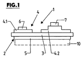
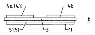
2 金属絶縁層基板
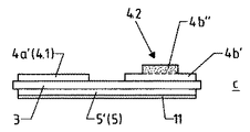
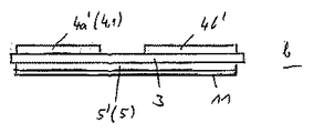
3 絶縁層
4 メタライゼーション
5 メタライゼーション
4.1 メタライゼーションエリア
4.2 メタライゼーションエリア
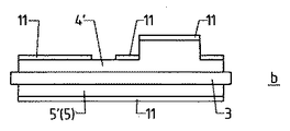
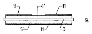
4’ 金属層または金属箔
4b’ 金属層
4b” 金属層
5 金属被覆
6 コンポーネント
7 コンポーネント
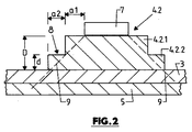
8 段
9 ライン
10 冷却器
11 保護層またはエッチングレジスト
a コンポーネント7とメタライゼーションエリア4.2の最上縁との間の間隔
a2 段8の幅
d メタライゼーション4および5のコンポーネント7の外側に備えられた部分エリア4.2.1の層の厚さ
D コンポーネント7の下側のメタライゼーション4の層の厚さ
b 層の厚さDおよびdの差
Claims (15)
- 電子装置、特に、電子回路または電子モジュールであって、少なくとも1つの、少なくとも絶縁層(3)および少なくとも1つの、前記絶縁層(3)表面側の第一のメタライゼーション(4)から成る金属絶縁層基板(2)を備え、該金属絶縁層基板の第一のメタライゼーション(4)がメタライゼーションエリア(4.1、4.2)を形成するために構造化されており、並びに少なくとも1つの、損失熱を発生させる電気または電子コンポーネント(7)を第一のメタライゼーション(4)の前記第一のメタライゼーションエリア(4.2)に備え、その際前記第一のメタライゼーションエリア(4.2)が、前記コンポーネント(7)と少なくとも熱的に接続されている部分エリア(4.2.1)のところに、層の厚さ(D)を備え、該層の厚さ(D)が前記第一の部分エリア(4.2.1)の前記第一のメタライゼーションエリア(4.2)の層の厚さ(d)より大幅に厚い装置において、前記層の厚さ(D、d)の差(b)が少なくとも前記第一の部分エリア(4.2.1)の外側の前記第一のメタライゼーションエリア(4.2)の前記層の厚さ(d)の半分と同じかまたはより大きく、および前記第一の部分エリア(4.2.1)の縁の前記コンポーネント(7)が備えている間隔(a1)が前記層の厚さ(D、d)の前記差(b)と同じまたはより大きいことを特徴とする、装置。
- 少なくとも1つの前記第一のメタライゼーションエリア(4.2)が、階段状に変化した層の厚さを備え、しかもより厚い前記層の厚さ(D)を備えた前記第一の部分エリア(4.2.1)が、より薄い前記層の厚さ(d)を備えた前記部分エリア(4.2.2)を少なくとも部分的に、好ましくはしかし完全に取り囲んでいることを特徴とする、請求項1に記載の装置。
- 前記第一のメタライゼーション(4)が、少なくとも1つの前記第一のメタライゼーションエリア(4.2)に追加して少なくとも1つの第二の構造化されたメ前記タライゼーションエリア(4.1)を備え、該メタライゼーションエリア(4.1)の層の厚さが前記第一の部分エリア(4.2.1)の前記層の厚さ(D)より小さく、好ましくは前記層の厚さ(d)と同じであり、該層の厚さ(d)がその前記第一の部分エリア(4.2.1)の外側に少なくとも1つの前記第一のメタライゼーションエリア(4)を備えていることを特徴とする、請求項1または2に記載の電子装置。
- 前記第一のメタライゼーション(4)と反対を向いた前記絶縁層(3)表面側に、第二のメタライゼーション(5)が好ましくは連続した、すなわち構造化されていない前記第二のメタライゼーション(5)が備えられていることを特徴とする、請求項1〜3のいずれか一項に記載の装置。
- 前記第一の部分エリア(4.2.1)の外の前記第一のメタライゼーション(4)の前記層の厚さおよび/または第二のメタライゼーション(5)の前記層の厚さが0.5mm〜0.8mmであることを特徴とする、請求項1〜4のいずれか一項に記載の装置。
- 前記絶縁層(3)の厚さが0.15mm〜1.0mmであることを特徴とする、請求項1〜5のいずれか一項に記載の装置。
- 前記絶縁層がセラミック層であり、好ましくはAl2O3、AlN、Si3N4、SiCまたはAl2O3+ZrO2から成るセラミック層であることを特徴とする、請求項1〜6のいずれか一項に記載の装置。
- 前記コンポーネント(7)に占められた面の寸法が5mm2〜180mm2、好ましくは9mm2〜150mm2であることを特徴とする、請求項1〜7のいずれか一項に記載の装置。
- 前記第一のおよび/または第二のメタライゼーションが銅、銅合金、アルミニウムまたはアルミニウム合金から成ることを特徴とする、請求項1〜8のいずれか一項に記載の装置。
- 前記損失熱を発生するコンポーネント(7)が、はんだ結合または焼結結合または接着結合によって前記第一のメタライゼーション(4)の前記第一のメタライゼーションエリア(4.2)と結合されていることを特徴とする、請求項1〜9のいずれか一項に記載の装置。
- 前記絶縁層が、例えば前記第二のメタライゼーション(5)を介して冷却器(10)と、例えばDCBボンディングによって、はんだ付けによって、また活性はんだによっても結合されることを特徴とする、請求項1〜10のいずれか一項に記載の装置。
- 前記第一のメタライゼーション(4)の前記メタライゼーションエリア(4.1、4.2)が、ステップエッチングによって作られることを特徴とする、請求項1〜11のいずれか一項に記載の装置。
- 前記第一の部分エリア(4.2.1)の前記層の厚さ(D)が、前記絶縁層(3)と結合された金属層(4’、4b’)上に追加の金属層(4b”)を施すことによる、すなわち例えば化学析出またはガルバニック析出による、および/またはレーザー焼結による、および/または金属薄板を施すことによることを特徴とする、請求項1〜12のいずれか一項に記載の装置。
- 少なくとも1つの前記第二のメタライゼーションエリア(4.1)が、導体を形成するためおよび/または接触表面を構造化するためであることを特徴とする、請求項1〜13のいずれか一項に記載の装置。
- 少なくとも1つの前記第二のメタライゼーションエリア(4.1)上に、好ましくは少なくとも1つの構造化された前記メタライゼーションエリア(4.1)上に、コンポーネント(6)が出力損失を低減して備えられていることを特徴とする、請求項1〜14のいずれか一項に記載の装置。
Applications Claiming Priority (3)
| Application Number | Priority Date | Filing Date | Title |
|---|---|---|---|
| DE102009033029A DE102009033029A1 (de) | 2009-07-02 | 2009-07-02 | Elektronische Vorrichtung |
| DE102009033029.1 | 2009-07-02 | ||
| PCT/DE2010/000745 WO2011000360A2 (de) | 2009-07-02 | 2010-06-29 | Elektronische vorrichtung |
Publications (1)
| Publication Number | Publication Date |
|---|---|
| JP2012531728A true JP2012531728A (ja) | 2012-12-10 |
Family
ID=42983560
Family Applications (1)
| Application Number | Title | Priority Date | Filing Date |
|---|---|---|---|
| JP2012516512A Pending JP2012531728A (ja) | 2009-07-02 | 2010-06-29 | 電子装置 |
Country Status (7)
| Country | Link |
|---|---|
| US (1) | US8749052B2 (ja) |
| EP (1) | EP2449586B1 (ja) |
| JP (1) | JP2012531728A (ja) |
| KR (1) | KR20120098575A (ja) |
| CN (1) | CN102484104B (ja) |
| DE (1) | DE102009033029A1 (ja) |
| WO (1) | WO2011000360A2 (ja) |
Cited By (10)
| Publication number | Priority date | Publication date | Assignee | Title |
|---|---|---|---|---|
| WO2015104954A1 (ja) * | 2014-01-10 | 2015-07-16 | 古河電気工業株式会社 | 電子回路装置 |
| JP2015520944A (ja) * | 2012-05-02 | 2015-07-23 | セラムテック ゲゼルシャフト ミット ベシュレンクテル ハフツングCeramTec GmbH | 金属が充填されたビアを有するセラミック基板からなるセラミックプリント基板を製造する方法 |
| WO2016163135A1 (ja) * | 2015-04-08 | 2016-10-13 | 三菱電機株式会社 | 電子モジュール及び電子装置 |
| WO2016190440A1 (ja) * | 2015-05-27 | 2016-12-01 | Ngkエレクトロデバイス株式会社 | パワーモジュール用基板およびパワーモジュール用基板集合体およびパワーモジュール用基板の製造方法 |
| JPWO2015022993A1 (ja) * | 2013-08-16 | 2017-03-02 | 日本碍子株式会社 | セラミック回路基板及び電子デバイス |
| JP2017199830A (ja) * | 2016-04-28 | 2017-11-02 | 三菱電機株式会社 | パワーモジュール |
| JPWO2022044541A1 (ja) * | 2020-08-28 | 2022-03-03 | ||
| WO2022162875A1 (ja) * | 2021-01-29 | 2022-08-04 | サンケン電気株式会社 | 半導体パワーモジュール |
| JP2025013227A (ja) * | 2023-07-12 | 2025-01-24 | 台達電子工業股▲ふん▼有限公司 | 半導体装置 |
| WO2025216198A1 (ja) * | 2024-04-08 | 2025-10-16 | 株式会社Niterra Materials | セラミックス銅接合体、セラミックス銅回路基板、およびセラミックス銅接合体の製造方法 |
Families Citing this family (63)
| Publication number | Priority date | Publication date | Assignee | Title |
|---|---|---|---|---|
| JP5860599B2 (ja) * | 2011-03-01 | 2016-02-16 | 昭和電工株式会社 | 絶縁回路基板、パワーモジュール用ベースおよびその製造方法 |
| WO2013059746A1 (en) | 2011-10-19 | 2013-04-25 | Nugen Technologies, Inc. | Compositions and methods for directional nucleic acid amplification and sequencing |
| DE102012102611B4 (de) * | 2012-02-15 | 2017-07-27 | Rogers Germany Gmbh | Metall-Keramik-Substrat sowie Verfahren zum Herstellen eines Metall-Keramik-Substrates |
| JP6192561B2 (ja) * | 2014-02-17 | 2017-09-06 | 三菱電機株式会社 | 電力用半導体装置 |
| JP6341822B2 (ja) | 2014-09-26 | 2018-06-13 | 三菱電機株式会社 | 半導体装置 |
| US11437304B2 (en) | 2014-11-06 | 2022-09-06 | Semiconductor Components Industries, Llc | Substrate structures and methods of manufacture |
| US9397017B2 (en) * | 2014-11-06 | 2016-07-19 | Semiconductor Components Industries, Llc | Substrate structures and methods of manufacture |
| US9408301B2 (en) | 2014-11-06 | 2016-08-02 | Semiconductor Components Industries, Llc | Substrate structures and methods of manufacture |
| JP6370257B2 (ja) | 2015-04-27 | 2018-08-08 | 三菱電機株式会社 | 半導体装置 |
| JP6582783B2 (ja) * | 2015-09-16 | 2019-10-02 | 富士電機株式会社 | 半導体装置 |
| EP3210957B1 (de) | 2016-02-26 | 2019-01-02 | Heraeus Deutschland GmbH & Co. KG | Kupfer-keramik-verbund |
| EP3210956B1 (de) | 2016-02-26 | 2018-04-11 | Heraeus Deutschland GmbH & Co. KG | Kupfer-keramik-verbund |
| EP3460838B1 (en) * | 2016-05-19 | 2021-02-24 | Mitsubishi Materials Corporation | Substrate for power modules |
| EP3261119A1 (en) * | 2016-06-21 | 2017-12-27 | Infineon Technologies AG | Power semiconductor module components and additive manufacturing thereof |
| KR101872257B1 (ko) | 2016-06-29 | 2018-06-28 | 박남철 | 마그넷 발전기 |
| KR101872262B1 (ko) | 2016-07-06 | 2018-08-02 | 박남철 | 마그넷 발전기 |
| JP7125931B2 (ja) | 2017-03-31 | 2022-08-25 | ローム株式会社 | パワーモジュールおよびその製造方法 |
| CN208369332U (zh) * | 2017-05-17 | 2019-01-11 | 德昌电机(深圳)有限公司 | 一种电机、电路板及应用该电机的引擎冷却模组 |
| EP3595002A1 (de) * | 2018-07-12 | 2020-01-15 | Heraeus Deutschland GmbH & Co KG | Metall-keramik-substrat mit einer zur direkten kühlung geformten folie als substratunterseite |
| DE102018212272A1 (de) * | 2018-07-24 | 2020-01-30 | Robert Bosch Gmbh | Keramischer Schaltungsträger und Elektronikeinheit |
| DE102018123681A1 (de) | 2018-09-26 | 2020-03-26 | Rogers Germany Gmbh | Trägersubstrat für elektrische, insbesondere elektronische Bauteile und Verfahren zum Herstellen eines Trägersubstrats |
| JP7147502B2 (ja) | 2018-11-19 | 2022-10-05 | 三菱電機株式会社 | 半導体装置、電力変換装置および半導体装置の製造方法 |
| DE102019108594A1 (de) | 2019-04-02 | 2020-10-08 | Rogers Germany Gmbh | Verfahren zur Herstellung eines Metall-Keramik-Subtrats und ein solches Metall-Keramik-Substrat. |
| DE102019113308A1 (de) | 2019-05-20 | 2020-11-26 | Rogers Germany Gmbh | Verfahren zur Herstellung eines Metall-Keramik-Substrats und Metall-Keramik- Substrat, hergestellt mit einem solchen Verfahren |
| US11387373B2 (en) * | 2019-07-29 | 2022-07-12 | Nxp Usa, Inc. | Low drain-source on resistance semiconductor component and method of fabrication |
| DE102019126954B4 (de) | 2019-10-08 | 2024-12-05 | Rogers Germany Gmbh | Verfahren zur Herstellung eines Metall-Keramik-Substrats, Lötsystem und Metall-Keramik-Substrat, hergestellt mit einem solchen Verfahren |
| DE102019135171A1 (de) | 2019-12-19 | 2021-06-24 | Rogers Germany Gmbh | Lotmaterial, Verfahren zur Herstellung eines solchen Lotmaterials und Verwendung eines solchen Lotmaterials zur Anbindung einer Metallschicht an eine Keramikschicht |
| DE102019135146B4 (de) | 2019-12-19 | 2022-11-24 | Rogers Germany Gmbh | Metall-Keramik-Substrat |
| DE102019135099A1 (de) | 2019-12-19 | 2021-06-24 | Rogers Germany Gmbh | Verfahren zur Herstellung eines Metall-Keramik-Substrats und Metall-Keramik-Substrat, hergestellt mit einem solchen Verfahren |
| DE102019135097A1 (de) | 2019-12-19 | 2021-06-24 | Rogers Germany Gmbh | Verfahren zur Herstellung eines Metall-Keramik-Substrats und Metall-Keramik-Substrat, hergestellt mit einem solchen Verfahren |
| DE102020202607A1 (de) * | 2020-02-28 | 2021-09-02 | Siemens Aktiengesellschaft | Elektronikmodul, Verfahren zur Herstellung eines Elektronikmoduls und Industrieanlage |
| DE102020106521A1 (de) | 2020-03-10 | 2021-09-16 | Rogers Germany Gmbh | Elektronikmodul und Verfahren zur Herstellung eines Elektronikmoduls |
| DE102020111698A1 (de) | 2020-04-29 | 2021-11-04 | Rogers Germany Gmbh | Verfahren zur Herstellung eines Metall-Keramik-Substrats und ein Metall-Keramik-Substrat hergestellt mit einem solchen Verfahren |
| DE102020111700B4 (de) | 2020-04-29 | 2024-12-05 | Rogers Germany Gmbh | Trägersubstrat und Verfahren zur Herstellung eines Trägersubstrats |
| DE102020111697A1 (de) | 2020-04-29 | 2021-11-04 | Rogers Germany Gmbh | Trägersubstrat und Verfahren zur Herstellung eines Trägersubstrats |
| DE102020112276A1 (de) * | 2020-05-06 | 2021-11-11 | Danfoss Silicon Power Gmbh | Leistungsmodul |
| DE102020205979A1 (de) | 2020-05-12 | 2021-11-18 | Robert Bosch Gesellschaft mit beschränkter Haftung | Leistungsmodul mit einer Wärmesenke |
| DE102020119209A1 (de) | 2020-07-21 | 2022-01-27 | Rogers Germany Gmbh | Leistungsmodul und Verfahren zur Herstellung eines Leistungsmoduls |
| DE102020119208A1 (de) | 2020-07-21 | 2022-01-27 | Rogers Germany Gmbh | Verfahren zur Herstellung eines Metall-Keramik-Substrats und Metall-Keramik-Substrat hergestellt mit einem solchen Verfahren |
| DE102020120189A1 (de) * | 2020-07-30 | 2022-02-03 | Rogers Germany Gmbh | Verfahren zur Herstellung eines Metall-Keramik-Substrats und ein Metall-Keramik-Substrat hergestellt mit einem solchen Verfahren |
| DE102020120188B4 (de) | 2020-07-30 | 2024-08-01 | Rogers Germany Gmbh | Verfahren zur Herstellung eines Trägersubstrats und ein Trägersubstrat hergestellt mit einem solchen Verfahren |
| DE102021100463A1 (de) | 2021-01-13 | 2022-07-14 | Rogers Germany Gmbh | Verfahren zum Herstellen eines Metall-Keramik-Substrats und Metall-Keramik-Substrat hergestellt mit einem solchen Verfahren |
| DE102021107690A1 (de) | 2021-03-26 | 2022-09-29 | Rogers Germany Gmbh | Verfahren zur Herstellung eines Metall-Keramik-Substrats und Metall-Keramik-Substrat hergestellt mit einem solchen Verfahren |
| DE102021107872A1 (de) | 2021-03-29 | 2022-09-29 | Rogers Germany Gmbh | Trägersubstrat für elektrische, insbesondere elektronische Bauteile und Verfahren zum Herstellen eines Trägersubstrats |
| DE102021125557A1 (de) | 2021-10-01 | 2023-04-06 | Rogers Germany Gmbh | Metall-Keramik-Substrat und Verfahren zur Herstellung eines Metall-Keramik-Substrats |
| DE102021126529B4 (de) | 2021-10-13 | 2025-11-13 | Rogers Germany Gmbh | Verfahren zur Herstellung von Metall-Keramik-Substraten |
| DE102022104156A1 (de) | 2022-02-22 | 2023-08-24 | Rogers Germany Gmbh | Metall-Keramik-Substrat und Verfahren zur Herstellung eines Metall-Keramik-Substrats |
| JP7707970B2 (ja) * | 2022-03-11 | 2025-07-15 | 三菱マテリアル株式会社 | ヒートシンク一体型絶縁回路基板、および、電子デバイス |
| EP4273928A1 (en) * | 2022-05-02 | 2023-11-08 | Infineon Technologies AG | A semiconductor package comprising power and logic on a single ceramic plate |
| EP4294135A1 (de) * | 2022-06-14 | 2023-12-20 | CeramTec GmbH | Metallische struktur als vorprodukt für elektrische schaltungen und verfahren zur herstellung einer elektrischen schaltung |
| DE102022119688B3 (de) | 2022-08-05 | 2024-02-08 | Rogers Germany Gmbh | Verfahren zum Herstellen eines Metall-Keramik-Substrats und Anlage für ein solches Verfahren |
| DE102022122799A1 (de) | 2022-09-08 | 2024-03-14 | Rogers Germany Gmbh | Elektronikmodul und Verfahren zur Herstellung eines solchen Elektronikmoduls |
| DE102022129493A1 (de) | 2022-11-08 | 2024-05-08 | Rogers Germany Gmbh | Metall-Keramik-Substrat und Verfahren zur Herstellung von Metall-Keramik-Substraten |
| DE102022134661A1 (de) | 2022-12-23 | 2024-07-04 | Rogers Germany Gmbh | Verfahren zur Herstellung eines Metall-Keramik-Substrats, Keramikelement sowie Metallschicht für ein solches Verfahren und Metall-Keramik-Substrat hergestellt mit einem solchen Verfahren |
| DE102023103509A1 (de) | 2023-02-14 | 2024-08-14 | Rogers Germany Gmbh | Verfahren zur Herstellung eines Metall-Keramik-Substrats und ein Metall-Keramik-Substrat hergestellt mit einem solchen Verfahren |
| DE102023103508A1 (de) | 2023-02-14 | 2024-08-14 | Rogers Germany Gmbh | Verfahren zur Herstellung eines Metall-Keramik-Substrats und ein Metall-Keramik-Substrat hergestellt mit einem solchen Verfahren |
| DE102023103850A1 (de) | 2023-02-16 | 2024-08-22 | Rogers Germany Gmbh | Metall-Keramik-Substrat und Verfahren zur Herstellung eines Metall-Keramik-Substrats |
| DE102023113512A1 (de) | 2023-05-24 | 2024-11-28 | Rogers Germany Gmbh | Trägersubstrat und Verfahren zur Herstellung eines Trägersubstrats |
| DE102023113513A1 (de) | 2023-05-24 | 2024-11-28 | Rogers Germany Gmbh | Metall-Keramik-Substrat und Verfahren zur Herstellung eines Metall-Keramik-Substrats |
| DE102023126070A1 (de) | 2023-09-26 | 2025-03-27 | Rogers Germany Gmbh | Verfahren zur Herstellung eines Metall-Keramik-Substrats und Metall-Keramik-Substrat |
| EP4576199A1 (en) * | 2023-12-20 | 2025-06-25 | Infineon Technologies AG | Substrate and methods for producing a substrate |
| US20260011629A1 (en) * | 2024-07-02 | 2026-01-08 | Semiconductor Components Industries, Llc | Substrate with stepped conductive layer surface |
| DE102024121939A1 (de) * | 2024-08-01 | 2026-02-05 | Kostal Automobil Elektrik Gmbh & Co. Kg | Anordnung zur Abführung elektrischer Verlustwärme eines elektrischen Leistungsbauteils |
Citations (2)
| Publication number | Priority date | Publication date | Assignee | Title |
|---|---|---|---|---|
| JP2006286754A (ja) * | 2005-03-31 | 2006-10-19 | Dowa Mining Co Ltd | 金属−セラミックス接合基板 |
| JP2006319146A (ja) * | 2005-05-13 | 2006-11-24 | Fuji Electric Holdings Co Ltd | 配線基板 |
Family Cites Families (21)
| Publication number | Priority date | Publication date | Assignee | Title |
|---|---|---|---|---|
| DE2213115C3 (de) | 1972-03-17 | 1975-12-04 | Siemens Ag, 1000 Berlin Und 8000 Muenchen | Verfahren zum hochfesten Verbinden von Keramiken aus Karbiden, einschließlich des Diamanten, Boriden, Nitriden oder Suiziden mit Metall nach dem Trocken-Lötverfahren |
| US3744120A (en) | 1972-04-20 | 1973-07-10 | Gen Electric | Direct bonding of metals with a metal-gas eutectic |
| US3766634A (en) | 1972-04-20 | 1973-10-23 | Gen Electric | Method of direct bonding metals to non-metallic substrates |
| JPH0810710B2 (ja) | 1984-02-24 | 1996-01-31 | 株式会社東芝 | 良熱伝導性基板の製造方法 |
| DE3922485C1 (ja) | 1989-07-08 | 1990-06-13 | Doduco Gmbh + Co Dr. Eugen Duerrwaechter, 7530 Pforzheim, De | |
| EP1132961B1 (en) * | 1991-07-24 | 2011-01-05 | Denki Kagaku Kogyo Kabushiki Kaisha | Method for producing a circuit substrate having a mounted semiconductor element |
| JPH07202063A (ja) | 1993-12-28 | 1995-08-04 | Toshiba Corp | セラミックス回路基板 |
| JP3957341B2 (ja) * | 1996-04-18 | 2007-08-15 | 日本インター株式会社 | 複合半導体装置 |
| EP0874399A1 (en) * | 1996-08-20 | 1998-10-28 | Kabushiki Kaisha Toshiba | Silicon nitride circuit board and semiconductor module |
| JP3512977B2 (ja) | 1996-08-27 | 2004-03-31 | 同和鉱業株式会社 | 高信頼性半導体用基板 |
| US6207221B1 (en) * | 1997-03-01 | 2001-03-27 | Jürgen Schulz-Harder | Process for producing a metal-ceramic substrate and a metal-ceramic substrate |
| EP0935286A4 (en) | 1997-05-26 | 2008-04-09 | Sumitomo Electric Industries | COPPER CIRCUIT CONNECTING SUBSTRATE AND ITS MANUFACTURE |
| JP4756200B2 (ja) * | 2000-09-04 | 2011-08-24 | Dowaメタルテック株式会社 | 金属セラミックス回路基板 |
| JP2002203942A (ja) * | 2000-12-28 | 2002-07-19 | Fuji Electric Co Ltd | パワー半導体モジュール |
| ES2717849T3 (es) * | 2001-03-08 | 2019-06-25 | Alstom Transp Tech | Sustrato para circuito electrónico de potencia y módulo electrónico de potencia que utiliza dicho sustrato |
| JP2004128510A (ja) * | 2002-10-05 | 2004-04-22 | Semikron Elektron Gmbh | 向上された絶縁強度を有するパワー半導体モジュール |
| DE10261402A1 (de) * | 2002-12-30 | 2004-07-15 | Schulz-Harder, Jürgen, Dr.-Ing. | Wärmesenke in Form einer Heat-Pipe sowie Verfahren zum Herstellen einer solchen Wärmesenke |
| SG162620A1 (en) * | 2003-04-15 | 2010-07-29 | Denki Kagaku Kogyo Kk | Metal base circuit board and its production process |
| DE10327530A1 (de) * | 2003-06-17 | 2005-01-20 | Electrovac Gesmbh | Vorrichtung mit wenigstens einer von einem zu kühlenden Funktionselement gebildeten Wärmequelle, mit wenigstens einer Wärmesenke und mit wenigstens einer Zwischenlage aus einer thermischen leitenden Masse zwischen der Wärmequelle und der Wärmesenke sowie thermische leitende Masse, insbesondere zur Verwendung bei einer solchen Vorrichtung |
| DE102005032076B3 (de) * | 2005-07-08 | 2007-02-08 | Infineon Technologies Ag | Verfahren zum Herstellen eines Schaltungsmoduls |
| TWI449137B (zh) * | 2006-03-23 | 2014-08-11 | 製陶技術創新製陶工程股份公司 | 構件或電路用的攜帶體 |
-
2009
- 2009-07-02 DE DE102009033029A patent/DE102009033029A1/de not_active Withdrawn
-
2010
- 2010-06-29 EP EP10744841.7A patent/EP2449586B1/de active Active
- 2010-06-29 US US13/381,518 patent/US8749052B2/en active Active
- 2010-06-29 KR KR1020127001415A patent/KR20120098575A/ko not_active Ceased
- 2010-06-29 JP JP2012516512A patent/JP2012531728A/ja active Pending
- 2010-06-29 WO PCT/DE2010/000745 patent/WO2011000360A2/de not_active Ceased
- 2010-06-29 CN CN201080029496.5A patent/CN102484104B/zh active Active
Patent Citations (2)
| Publication number | Priority date | Publication date | Assignee | Title |
|---|---|---|---|---|
| JP2006286754A (ja) * | 2005-03-31 | 2006-10-19 | Dowa Mining Co Ltd | 金属−セラミックス接合基板 |
| JP2006319146A (ja) * | 2005-05-13 | 2006-11-24 | Fuji Electric Holdings Co Ltd | 配線基板 |
Cited By (19)
| Publication number | Priority date | Publication date | Assignee | Title |
|---|---|---|---|---|
| JP2015520944A (ja) * | 2012-05-02 | 2015-07-23 | セラムテック ゲゼルシャフト ミット ベシュレンクテル ハフツングCeramTec GmbH | 金属が充填されたビアを有するセラミック基板からなるセラミックプリント基板を製造する方法 |
| JPWO2015022993A1 (ja) * | 2013-08-16 | 2017-03-02 | 日本碍子株式会社 | セラミック回路基板及び電子デバイス |
| WO2015104954A1 (ja) * | 2014-01-10 | 2015-07-16 | 古河電気工業株式会社 | 電子回路装置 |
| JPWO2015104954A1 (ja) * | 2014-01-10 | 2017-03-23 | 古河電気工業株式会社 | 電子回路装置 |
| JPWO2016163135A1 (ja) * | 2015-04-08 | 2017-04-27 | 三菱電機株式会社 | 電子モジュール及び電子装置 |
| WO2016163135A1 (ja) * | 2015-04-08 | 2016-10-13 | 三菱電機株式会社 | 電子モジュール及び電子装置 |
| JPWO2016190440A1 (ja) * | 2015-05-27 | 2018-03-15 | Ngkエレクトロデバイス株式会社 | パワーモジュール用基板およびパワーモジュール用基板集合体およびパワーモジュール用基板の製造方法 |
| WO2016190440A1 (ja) * | 2015-05-27 | 2016-12-01 | Ngkエレクトロデバイス株式会社 | パワーモジュール用基板およびパワーモジュール用基板集合体およびパワーモジュール用基板の製造方法 |
| US10937715B2 (en) | 2015-05-27 | 2021-03-02 | NGK Electronics Devices, Inc. | Substrate for power module, collective substrate for power modules, and method for manufacturing substrate for power module |
| JP2017199830A (ja) * | 2016-04-28 | 2017-11-02 | 三菱電機株式会社 | パワーモジュール |
| JPWO2022044541A1 (ja) * | 2020-08-28 | 2022-03-03 | ||
| WO2022044541A1 (ja) * | 2020-08-28 | 2022-03-03 | 富士電機株式会社 | 半導体装置 |
| JP2024003177A (ja) * | 2020-08-28 | 2024-01-11 | 富士電機株式会社 | 半導体装置 |
| JP7428261B2 (ja) | 2020-08-28 | 2024-02-06 | 富士電機株式会社 | 半導体装置 |
| JP7729368B2 (ja) | 2020-08-28 | 2025-08-26 | 富士電機株式会社 | 半導体装置 |
| US12469792B2 (en) | 2020-08-28 | 2025-11-11 | Fuji Electric Co., Ltd. | Semiconductor device |
| WO2022162875A1 (ja) * | 2021-01-29 | 2022-08-04 | サンケン電気株式会社 | 半導体パワーモジュール |
| JP2025013227A (ja) * | 2023-07-12 | 2025-01-24 | 台達電子工業股▲ふん▼有限公司 | 半導体装置 |
| WO2025216198A1 (ja) * | 2024-04-08 | 2025-10-16 | 株式会社Niterra Materials | セラミックス銅接合体、セラミックス銅回路基板、およびセラミックス銅接合体の製造方法 |
Also Published As
| Publication number | Publication date |
|---|---|
| US8749052B2 (en) | 2014-06-10 |
| EP2449586B1 (de) | 2020-10-21 |
| EP2449586A2 (de) | 2012-05-09 |
| CN102484104B (zh) | 2016-01-27 |
| WO2011000360A3 (de) | 2011-03-17 |
| CN102484104A (zh) | 2012-05-30 |
| KR20120098575A (ko) | 2012-09-05 |
| US20120134115A1 (en) | 2012-05-31 |
| WO2011000360A2 (de) | 2011-01-06 |
| DE102009033029A1 (de) | 2011-01-05 |
Similar Documents
| Publication | Publication Date | Title |
|---|---|---|
| JP2012531728A (ja) | 電子装置 | |
| KR101188150B1 (ko) | 냉각 장치 | |
| US8963321B2 (en) | Semiconductor device including cladded base plate | |
| EP2200080B1 (en) | Low Cost Manufacturing of Micro-Channel Heatsink | |
| CN104603933B (zh) | 功率模块用基板及功率模块 | |
| EP3306655B1 (en) | Substrate for power modules, substrate assembly for power modules, and method for producing substrate for power modules | |
| US8559475B2 (en) | Heat sink and assembly or module unit | |
| JP5125241B2 (ja) | パワーモジュール用基板の製造方法 | |
| JP2013062506A (ja) | クラッド型ベースプレートを含む半導体装置 | |
| WO2009116439A1 (ja) | ヒートシンク付パワーモジュール用基板及びその製造方法、並びに、ヒートシンク付パワーモジュール、パワーモジュール用基板 | |
| US12035477B2 (en) | Electronic module and method for producing an electronic module | |
| US11476640B2 (en) | Adapter element for connecting a component, such as a laser diode, to a heat sink, a system comprising a laser diode, a heat sink and an adapter element and method for producing an adapter element | |
| JP6681660B2 (ja) | ヒートシンク付パワーモジュール用基板及びパワーモジュール | |
| JP6503796B2 (ja) | ヒートシンク付パワーモジュール用基板及びパワーモジュール | |
| JP6317178B2 (ja) | 回路基板および電子装置 | |
| JP3934966B2 (ja) | セラミック回路基板 | |
| JP6392583B2 (ja) | 回路基板、および電子装置 | |
| JP2014143342A (ja) | 半導体モジュール及びその製造方法 | |
| JP2022171153A (ja) | 半導体モジュール | |
| JP6819385B2 (ja) | 半導体装置の製造方法 | |
| US20240347417A1 (en) | Device comprising a ceramic substrate and method for producing same | |
| KR102930091B1 (ko) | 반도체 패키지 | |
| US12087660B2 (en) | Metal-ceramic substrate with a foil formed for direct cooling as substrate bottom | |
| JP2013211288A (ja) | ヒートシンク付パワーモジュール用基板の製造方法 | |
| CN116913885A (zh) | 半导体器件组件 |
Legal Events
| Date | Code | Title | Description |
|---|---|---|---|
| A621 | Written request for application examination |
Free format text: JAPANESE INTERMEDIATE CODE: A621 Effective date: 20130328 |
|
| A521 | Request for written amendment filed |
Free format text: JAPANESE INTERMEDIATE CODE: A523 Effective date: 20130612 |
|
| A977 | Report on retrieval |
Free format text: JAPANESE INTERMEDIATE CODE: A971007 Effective date: 20131031 |
|
| A601 | Written request for extension of time |
Free format text: JAPANESE INTERMEDIATE CODE: A601 Effective date: 20140205 |
|
| A601 | Written request for extension of time |
Free format text: JAPANESE INTERMEDIATE CODE: A601 Effective date: 20140305 |
|
| A521 | Request for written amendment filed |
Free format text: JAPANESE INTERMEDIATE CODE: A523 Effective date: 20140314 |
|
| A521 | Request for written amendment filed |
Free format text: JAPANESE INTERMEDIATE CODE: A523 Effective date: 20140403 |
|
| A602 | Written permission of extension of time |
Free format text: JAPANESE INTERMEDIATE CODE: A602 Effective date: 20140409 Free format text: JAPANESE INTERMEDIATE CODE: A602 Effective date: 20140227 |
|
| A02 | Decision of refusal |
Free format text: JAPANESE INTERMEDIATE CODE: A02 Effective date: 20150106 |