JP2013033962A - 基板処理装置及び基板処理方法 - Google Patents
基板処理装置及び基板処理方法 Download PDFInfo
- Publication number
- JP2013033962A JP2013033962A JP2012163299A JP2012163299A JP2013033962A JP 2013033962 A JP2013033962 A JP 2013033962A JP 2012163299 A JP2012163299 A JP 2012163299A JP 2012163299 A JP2012163299 A JP 2012163299A JP 2013033962 A JP2013033962 A JP 2013033962A
- Authority
- JP
- Japan
- Prior art keywords
- substrate
- housing
- supply port
- substrate processing
- supercritical fluid
- Prior art date
- Legal status (The legal status is an assumption and is not a legal conclusion. Google has not performed a legal analysis and makes no representation as to the accuracy of the status listed.)
- Granted
Links
Images




Classifications
-
- H—ELECTRICITY
- H10—SEMICONDUCTOR DEVICES; ELECTRIC SOLID-STATE DEVICES NOT OTHERWISE PROVIDED FOR
- H10P—GENERIC PROCESSES OR APPARATUS FOR THE MANUFACTURE OR TREATMENT OF DEVICES COVERED BY CLASS H10
- H10P72/00—Handling or holding of wafers, substrates or devices during manufacture or treatment thereof
- H10P72/04—Apparatus for manufacture or treatment
- H10P72/0402—Apparatus for fluid treatment
- H10P72/0406—Apparatus for fluid treatment for cleaning followed by drying, rinsing, stripping, blasting or the like
-
- F—MECHANICAL ENGINEERING; LIGHTING; HEATING; WEAPONS; BLASTING
- F26—DRYING
- F26B—DRYING SOLID MATERIALS OR OBJECTS BY REMOVING LIQUID THEREFROM
- F26B25/00—Details of general application not covered by group F26B21/00 or F26B23/00
- F26B25/06—Chambers, containers, or receptacles
- F26B25/14—Chambers, containers, receptacles of simple construction
-
- H—ELECTRICITY
- H10—SEMICONDUCTOR DEVICES; ELECTRIC SOLID-STATE DEVICES NOT OTHERWISE PROVIDED FOR
- H10P—GENERIC PROCESSES OR APPARATUS FOR THE MANUFACTURE OR TREATMENT OF DEVICES COVERED BY CLASS H10
- H10P72/00—Handling or holding of wafers, substrates or devices during manufacture or treatment thereof
- H10P72/04—Apparatus for manufacture or treatment
- H10P72/0402—Apparatus for fluid treatment
- H10P72/0406—Apparatus for fluid treatment for cleaning followed by drying, rinsing, stripping, blasting or the like
- H10P72/0408—Apparatus for fluid treatment for cleaning followed by drying, rinsing, stripping, blasting or the like for drying
-
- H—ELECTRICITY
- H10—SEMICONDUCTOR DEVICES; ELECTRIC SOLID-STATE DEVICES NOT OTHERWISE PROVIDED FOR
- H10P—GENERIC PROCESSES OR APPARATUS FOR THE MANUFACTURE OR TREATMENT OF DEVICES COVERED BY CLASS H10
- H10P72/00—Handling or holding of wafers, substrates or devices during manufacture or treatment thereof
- H10P72/04—Apparatus for manufacture or treatment
- H10P72/0402—Apparatus for fluid treatment
- H10P72/0406—Apparatus for fluid treatment for cleaning followed by drying, rinsing, stripping, blasting or the like
- H10P72/0411—Apparatus for fluid treatment for cleaning followed by drying, rinsing, stripping, blasting or the like for wet cleaning or washing
- H10P72/0414—Apparatus for fluid treatment for cleaning followed by drying, rinsing, stripping, blasting or the like for wet cleaning or washing using mainly spraying means, e.g. nozzles
-
- H—ELECTRICITY
- H10—SEMICONDUCTOR DEVICES; ELECTRIC SOLID-STATE DEVICES NOT OTHERWISE PROVIDED FOR
- H10P—GENERIC PROCESSES OR APPARATUS FOR THE MANUFACTURE OR TREATMENT OF DEVICES COVERED BY CLASS H10
- H10P72/00—Handling or holding of wafers, substrates or devices during manufacture or treatment thereof
- H10P72/04—Apparatus for manufacture or treatment
- H10P72/0431—Apparatus for thermal treatment
- H10P72/0434—Apparatus for thermal treatment mainly by convection
-
- H—ELECTRICITY
- H10—SEMICONDUCTOR DEVICES; ELECTRIC SOLID-STATE DEVICES NOT OTHERWISE PROVIDED FOR
- H10P—GENERIC PROCESSES OR APPARATUS FOR THE MANUFACTURE OR TREATMENT OF DEVICES COVERED BY CLASS H10
- H10P72/00—Handling or holding of wafers, substrates or devices during manufacture or treatment thereof
- H10P72/04—Apparatus for manufacture or treatment
- H10P72/0441—Apparatus for sealing, encapsulating, glassing, decapsulating or the like
-
- H—ELECTRICITY
- H10—SEMICONDUCTOR DEVICES; ELECTRIC SOLID-STATE DEVICES NOT OTHERWISE PROVIDED FOR
- H10P—GENERIC PROCESSES OR APPARATUS FOR THE MANUFACTURE OR TREATMENT OF DEVICES COVERED BY CLASS H10
- H10P72/00—Handling or holding of wafers, substrates or devices during manufacture or treatment thereof
- H10P72/04—Apparatus for manufacture or treatment
- H10P72/0451—Apparatus for manufacturing or treating in a plurality of work-stations
- H10P72/0452—Apparatus for manufacturing or treating in a plurality of work-stations characterised by the layout of the process chambers
- H10P72/0458—Apparatus for manufacturing or treating in a plurality of work-stations characterised by the layout of the process chambers vertical arrangement
-
- H—ELECTRICITY
- H10—SEMICONDUCTOR DEVICES; ELECTRIC SOLID-STATE DEVICES NOT OTHERWISE PROVIDED FOR
- H10P—GENERIC PROCESSES OR APPARATUS FOR THE MANUFACTURE OR TREATMENT OF DEVICES COVERED BY CLASS H10
- H10P72/00—Handling or holding of wafers, substrates or devices during manufacture or treatment thereof
- H10P72/04—Apparatus for manufacture or treatment
- H10P72/0451—Apparatus for manufacturing or treating in a plurality of work-stations
- H10P72/0462—Apparatus for manufacturing or treating in a plurality of work-stations characterised by the construction of the processing chambers, e.g. modular processing chambers
-
- H—ELECTRICITY
- H10—SEMICONDUCTOR DEVICES; ELECTRIC SOLID-STATE DEVICES NOT OTHERWISE PROVIDED FOR
- H10P—GENERIC PROCESSES OR APPARATUS FOR THE MANUFACTURE OR TREATMENT OF DEVICES COVERED BY CLASS H10
- H10P72/00—Handling or holding of wafers, substrates or devices during manufacture or treatment thereof
- H10P72/30—Handling or holding of wafers, substrates or devices during manufacture or treatment thereof for conveying, e.g. between different workstations
- H10P72/33—Handling or holding of wafers, substrates or devices during manufacture or treatment thereof for conveying, e.g. between different workstations into and out of processing chamber
- H10P72/3306—Horizontal transfer of a single workpiece
-
- H—ELECTRICITY
- H10—SEMICONDUCTOR DEVICES; ELECTRIC SOLID-STATE DEVICES NOT OTHERWISE PROVIDED FOR
- H10P—GENERIC PROCESSES OR APPARATUS FOR THE MANUFACTURE OR TREATMENT OF DEVICES COVERED BY CLASS H10
- H10P72/00—Handling or holding of wafers, substrates or devices during manufacture or treatment thereof
- H10P72/70—Handling or holding of wafers, substrates or devices during manufacture or treatment thereof for supporting or gripping
- H10P72/76—Handling or holding of wafers, substrates or devices during manufacture or treatment thereof for supporting or gripping using mechanical means, e.g. clamps or pinches
- H10P72/7604—Handling or holding of wafers, substrates or devices during manufacture or treatment thereof for supporting or gripping using mechanical means, e.g. clamps or pinches the wafers being placed on a susceptor, stage or support
- H10P72/7614—Handling or holding of wafers, substrates or devices during manufacture or treatment thereof for supporting or gripping using mechanical means, e.g. clamps or pinches the wafers being placed on a susceptor, stage or support characterised by a plurality of individual support members, e.g. support posts or protrusions
Landscapes
- Engineering & Computer Science (AREA)
- Mechanical Engineering (AREA)
- General Engineering & Computer Science (AREA)
- Cleaning Or Drying Semiconductors (AREA)
Abstract
【解決手段】本発明による基板処理装置の一実施形態は、工程が遂行される空間を提供するハウジング4100と、ハウジング4100の内部に基板Sを支持する支持部材4300と、ハウジング4100へ工程流体を供給する供給ポートと、供給ポートと支持部材4300との間に配置されて工程流体が基板Sへ直接噴射されることを遮断する遮断プレート4610を含む遮断部材4600と、ハウジング4100から工程流体を排気する排出ポート4700と、を含む。
【選択図】図4
Description
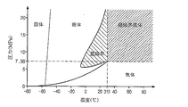
前記超臨界流体は、超臨界二酸化炭素であり得る。
1000・・・インデックスモジュール
1100・・・ロードポート
1200・・・移送フレーム
1210・・・インデックスロボット
1220・・・インデックスレール
2000・・・工程モジュール
2100・・・バッファチャンバー
2200・・・移送チャンバー
2210・・・移送ロボット
2220・・・移送レール
3000・・・第1工程チャンバー
3100・・・支持部材
3110・・・支持プレート
3111・・・支持ピン
3112・・・チャッキングピン
3120・・・回転軸
3130・・・回転駆動器
3200・・・ノズル部材
3210・・・ノズル
3220・・・ノズルバー
3230・・・ノズル軸
3240・・・ノズル軸駆動器
3300・・・回収部材
3310・・・回収筒
3311・・・回収口
3320・・・回収ライン
3330・・・乗降バー
3340・・・乗降駆動器
4000・・・第2工程チャンバー
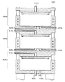
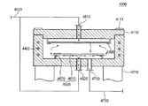
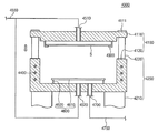
4100・・・ハウジング
4110・・・上部ハウジング
4111・・・水平調整部材
4120・・・下部ハウジング
4130・・・ドア
4200・・・乗降部材
4210・・・乗降シリンダー
4220・・・乗降ロード
4300・・・支持部材
4400・・・加熱部材
4510・・・上部供給ポート
4520・・・下部供給ポート
4600・・・遮断部材
4610・・・遮断プレート
4620・・・支持台
4700・・・排気ポート
4800・・・加圧部材
4810・・・加圧シリンダー
4820・・・加圧ロード
4821・・・ロードヘッド
C・・・容器
S・・・基板
Claims (22)
- 工程が遂行される空間を提供するハウジングと、
前記ハウジングの内部に基板を支持する支持部材と、
前記ハウジングへ工程流体を供給する供給ポートと、
前記供給ポートと前記支持部材との間に配置されて前記工程流体が前記基板へ直接噴射されることを遮断する遮断プレートを含む遮断部材と、
前記ハウジングから前記工程流体を排気する排出ポートと、を含む基板処理装置。 - 前記供給ポートは、前記ハウジングの互いに異なる面に形成される第1供給ポート及び第2供給ポートを含み、
前記遮断プレートは、前記支持部材と前記第1供給ポートとの間に配置される請求項1に記載の基板処理装置。 - 前記第1供給ポートは、前記ハウジングの下部に形成されて前記基板の下面中央部に向かって前記工程流体を噴射し、
前記第2供給ポートは、前記ハウジングの上部に形成されて前記基板の上面中央部に向かって前記工程流体を噴射する請求項2に記載の基板処理装置。 - 前記第1供給ポートが前記工程流体を供給した後、前記第2供給ポートが前記工程流体を供給するように制御する制御器をさらに含む請求項3に記載の基板処理装置。
- 前記遮断部材は、前記ハウジングの下部から延長される支持台をさらに含み、
前記遮断プレートは、前記支持台の上に安着される請求項3に記載の基板処理装置。 - 前記遮断プレートの半径は、前記基板の半径より大きく提供される請求項1に記載の基板処理装置。
- 前記工程は超臨界工程であり、
前記工程流体は、超臨界流体相(supercritical fluid phase)である請求項1に記載の基板処理装置。 - 前記ハウジングは、上部ハウジング及び前記上部ハウジングの下に配置される下部ハウジングを含み、
前記上部ハウジング又は前記下部ハウジングのうちいずれか1つを昇降させる乗降部材をさらに含む請求項1乃至請求項7のいずれかに記載の基板処理装置。 - 前記支持部材は、前記上部ハウジングから下方に延長され、その下端で水平方向に折曲されて前記基板の縁領域を支持する請求項8に記載の基板処理装置。
- 前記上部ハウジングの水平度を調整する水平調整部材をさらに含む請求項9に記載の基板処理装置。
- 前記第1供給ポートは、前記下部ハウジングに形成され、
前記第2供給ポートは、前記上部ハウジングに形成される請求項8に記載の基板処理装置。 - 前記ハウジングは、一側が開放され、上下に移動して前記開放された一側を開閉するドアを含む請求項1乃至請求項7のいずれかに記載の基板処理装置。
- 前記ハウジングが密閉されるように前記ドアに圧力を加える加圧部材をさらに含む請求項12に記載の基板処理装置。
- ハウジングへ基板を搬入して支持部材に安着させる段階と、
前記ハウジングへ工程流体を供給する段階と、
前記工程流体が前記基板へ直接噴射されることを遮断する段階と、
前記ハウジングから前記工程流体を排気する段階と、
前記ハウジングから前記基板を搬出する段階と、を含む基板処理方法。 - 前記遮断する段階は、前記工程流体を供給する供給ポートと前記支持部材との間に配置される遮断プレートが前記工程流体を遮断する請求項14に記載の基板処理方法。
- 前記供給する段階は、前記ハウジングの上部に形成された第1供給ポートが前記基板の上面に向かって前記工程流体を噴射し、前記ハウジングの下部に形成された第2供給ポートが前記基板の下面に向かって前記工程流体を噴射し、
前記遮断する段階は、前記遮断プレートが前記第2供給ポートと前記支持部材との間に配置されて前記基板の下面に噴射される工程流体が前記基板へ直接噴射されることを遮断する請求項15に記載の基板処理方法。 - 前記供給する段階は、前記第2供給ポートが前記工程流体を噴射して前記ハウジングの内部圧力が予め設定された圧力に到達すれば、前記第1供給ポートが前記工程流体の噴射を開始する請求項16に記載の基板処理方法。
- 前記工程流体は、超臨界流体であり、
前記超臨界流体によって前記基板に残留する有機溶剤が溶解されて前記基板が乾燥される請求項14乃至請求項17のいずれかに記載の基板処理方法。 - 前記ハウジングは、上部ハウジング及び前記上部ハウジングの下に配置される下部ハウジングを含み、
前記基板は、前記上部ハウジングと前記下部ハウジングとが離隔された状態で前記支持部材に安着され、
前記基板が搬入されれば、前記上部ハウジング及び前記下部ハウジングのうち1つを乗降させて前記ハウジングを密閉する段階をさらに含む請求項14乃至請求項17のいずれかに記載の基板処理方法。 - 有機溶剤が残留する基板をハウジングへ搬入し、超臨界流体が前記基板へ直接噴射されることを遮断し、前記基板の非パターン面に向かって超臨界流体を供給し、前記ハウジング内に超臨界雰囲気を造成し、前記超臨界雰囲気が造成されれば、前記基板のパターン面に向かって前記超臨界流体を噴射して前記基板の回路パターンの間に残留する有機溶剤を溶解させて前記基板を乾燥する基板処理方法。
- 前記基板の非パターン面に向かって前記超臨界流体が噴射される経路上に配置された遮断プレートが前記超臨界流体が前記基板へ直接噴射されることを防止する請求項20に記載の基板処理方法。
- 前記超臨界流体は、超臨界二酸化炭素である請求項20又は請求項21に記載の基板処理方法。
Applications Claiming Priority (4)
| Application Number | Priority Date | Filing Date | Title |
|---|---|---|---|
| KR20110076241 | 2011-07-29 | ||
| KR10-2011-0076241 | 2011-07-29 | ||
| KR1020110140015A KR101329304B1 (ko) | 2011-07-29 | 2011-12-22 | 기판처리장치 및 기판처리방법 |
| KR10-2011-0140015 | 2011-12-22 |
Publications (2)
| Publication Number | Publication Date |
|---|---|
| JP2013033962A true JP2013033962A (ja) | 2013-02-14 |
| JP5686261B2 JP5686261B2 (ja) | 2015-03-18 |
Family
ID=47596028
Family Applications (1)
| Application Number | Title | Priority Date | Filing Date |
|---|---|---|---|
| JP2012163299A Active JP5686261B2 (ja) | 2011-07-29 | 2012-07-24 | 基板処理装置及び基板処理方法 |
Country Status (2)
| Country | Link |
|---|---|
| US (3) | US9984902B2 (ja) |
| JP (1) | JP5686261B2 (ja) |
Cited By (24)
| Publication number | Priority date | Publication date | Assignee | Title |
|---|---|---|---|---|
| JP2014175669A (ja) * | 2013-03-12 | 2014-09-22 | Samsung Electronics Co Ltd | 超臨界流体を利用する基板処理装置、及びこれを含む基板処理システム |
| JP2018074103A (ja) * | 2016-11-04 | 2018-05-10 | 東京エレクトロン株式会社 | 基板処理装置、基板処理方法及び記録媒体 |
| JP2018530921A (ja) * | 2015-10-04 | 2018-10-18 | アプライド マテリアルズ インコーポレイテッドApplied Materials,Incorporated | 熱質量が小さい加圧チャンバ |
| JP2018534770A (ja) * | 2015-10-04 | 2018-11-22 | アプライド マテリアルズ インコーポレイテッドApplied Materials,Incorporated | 基板支持とバッフルの装置 |
| KR20180134179A (ko) * | 2017-06-08 | 2018-12-18 | 삼성전자주식회사 | 기판 처리 장치 및 집적회로 소자 제조 장치 |
| US10777405B2 (en) | 2015-10-04 | 2020-09-15 | Applied Materials, Inc. | Drying process for high aspect ratio features |
| JP2021009875A (ja) * | 2019-06-28 | 2021-01-28 | 株式会社Screenホールディングス | 基板処理装置 |
| WO2021112130A1 (ja) * | 2019-12-06 | 2021-06-10 | 株式会社レクザム | ウェハ処理装置 |
| JP2021093389A (ja) * | 2019-12-06 | 2021-06-17 | 株式会社レクザム | ウェハ処理装置 |
| JP2021116201A (ja) * | 2020-01-24 | 2021-08-10 | 国立大学法人東海国立大学機構 | 薄膜形成方法 |
| JP2021125576A (ja) * | 2020-02-06 | 2021-08-30 | 株式会社レクザム | ウェハ処理装置 |
| JP2021125667A (ja) * | 2020-02-10 | 2021-08-30 | 株式会社レクザム | ウェハ処理装置 |
| US11133174B2 (en) | 2015-10-04 | 2021-09-28 | Applied Materials, Inc. | Reduced volume processing chamber |
| KR20220006385A (ko) * | 2020-07-08 | 2022-01-17 | 세메스 주식회사 | 기판 처리 장치 및 방법 |
| JP2022030850A (ja) * | 2020-08-07 | 2022-02-18 | 東京エレクトロン株式会社 | 基板処理装置、及び基板処理方法 |
| JP2022030851A (ja) * | 2020-08-07 | 2022-02-18 | 東京エレクトロン株式会社 | 基板処理装置、及び基板処理方法 |
| US20220186379A1 (en) * | 2020-12-10 | 2022-06-16 | Semes Co., Ltd. | Substrate treating apparatus and filler member provided therein |
| JP2022104862A (ja) * | 2020-12-30 | 2022-07-12 | セメス株式会社 | 支持装置、及び支持装置を含む基板処理装置 |
| KR20220162216A (ko) * | 2021-05-31 | 2022-12-08 | 세메스 주식회사 | 기판 처리 장치 |
| JP2024015413A (ja) * | 2018-01-04 | 2024-02-01 | 東京エレクトロン株式会社 | 基板処理装置 |
| US11894346B2 (en) | 2016-02-22 | 2024-02-06 | Samsung Electronics Co., Ltd. | Semiconductor package having a high reliability |
| JP2024045869A (ja) * | 2022-09-22 | 2024-04-03 | 株式会社Screenホールディングス | 基板処理装置および基板処理方法 |
| KR20240114699A (ko) | 2023-01-17 | 2024-07-24 | 도쿄엘렉트론가부시키가이샤 | 기판 처리 장치 및 기판 처리 장치의 메인터넌스 방법 |
| KR20240114700A (ko) | 2023-01-17 | 2024-07-24 | 도쿄엘렉트론가부시키가이샤 | 기판 처리 장치 및 기판 처리 장치의 메인터넌스 방법 |
Families Citing this family (16)
| Publication number | Priority date | Publication date | Assignee | Title |
|---|---|---|---|---|
| KR101874901B1 (ko) | 2011-12-07 | 2018-07-06 | 삼성전자주식회사 | 기판 건조 장치 및 방법 |
| JP6302700B2 (ja) | 2013-03-18 | 2018-03-28 | 芝浦メカトロニクス株式会社 | 基板処理装置及び基板処理方法 |
| JP6351993B2 (ja) | 2013-03-18 | 2018-07-04 | 芝浦メカトロニクス株式会社 | 基板処理装置及び基板処理方法 |
| JP6455962B2 (ja) * | 2013-03-18 | 2019-01-23 | 芝浦メカトロニクス株式会社 | 基板処理装置及び基板処理方法 |
| TWI661479B (zh) * | 2015-02-12 | 2019-06-01 | Screen Holdings Co,. Ltd. | 基板處理裝置、基板處理系統以及基板處理方法 |
| CN105207408B (zh) * | 2015-10-26 | 2018-01-30 | 深圳市道通智能航空技术有限公司 | 一种电机、云台及飞行器 |
| KR102669903B1 (ko) * | 2016-08-30 | 2024-05-28 | 주성엔지니어링(주) | 기판 처리 장치 |
| KR102603528B1 (ko) | 2016-12-29 | 2023-11-17 | 삼성전자주식회사 | 기판 처리 장치 및 이를 포함한 기판 처리 시스템 |
| KR101987949B1 (ko) * | 2017-10-16 | 2019-06-11 | 세메스 주식회사 | 기판 처리 장치 및 기판 처리 방법 |
| US20190164787A1 (en) * | 2017-11-30 | 2019-05-30 | Semes Co., Ltd. | Apparatus and method for processing substrate |
| KR102042789B1 (ko) * | 2017-11-30 | 2019-11-08 | 세메스 주식회사 | 기판 처리 방법 및 기판 처리 장치 |
| JP7210960B2 (ja) * | 2018-09-21 | 2023-01-24 | 東京エレクトロン株式会社 | 真空処理装置及び基板搬送方法 |
| KR102387088B1 (ko) * | 2019-10-31 | 2022-04-15 | 세메스 주식회사 | 기판 처리 장치 |
| US11640115B2 (en) | 2020-09-04 | 2023-05-02 | Samsung Electronics Co., Ltd. | Substrate processing apparatus, semiconductor manufacturing equipment, and substrate processing method |
| KR20240014906A (ko) * | 2022-07-26 | 2024-02-02 | 삼성전자주식회사 | 기판 처리 장치 및 기판 처리 방법 |
| CN117928179B (zh) * | 2022-10-14 | 2025-12-19 | 盛美半导体设备(上海)股份有限公司 | 使用超临界流体对基板进行干燥的干燥装置及方法 |
Citations (10)
| Publication number | Priority date | Publication date | Assignee | Title |
|---|---|---|---|---|
| JP2001324263A (ja) * | 2000-05-15 | 2001-11-22 | Nippon Telegr & Teleph Corp <Ntt> | 超臨界乾燥装置 |
| JP2002320929A (ja) * | 2001-04-27 | 2002-11-05 | Kobe Steel Ltd | 高圧処理方法及び高圧処理装置 |
| JP2003142368A (ja) * | 2001-10-31 | 2003-05-16 | Matsushita Electric Ind Co Ltd | パターン形成方法 |
| JP2004146457A (ja) * | 2002-10-22 | 2004-05-20 | Kobe Steel Ltd | 高圧処理方法および高圧処理装置 |
| JP2004186530A (ja) * | 2002-12-05 | 2004-07-02 | Sony Corp | 洗浄装置及び洗浄方法 |
| JP2006303316A (ja) * | 2005-04-22 | 2006-11-02 | Ntt Advanced Technology Corp | 超臨界処理方法及び装置 |
| JP2007305676A (ja) * | 2006-05-09 | 2007-11-22 | Sony Corp | 基板の処理方法及び処理装置 |
| JP2008072118A (ja) * | 2006-09-12 | 2008-03-27 | Semes Co Ltd | 超臨界流体を用いる基板乾燥装置及びこれを備える基板処理設備並びに基板処理方法 |
| JP2008306175A (ja) * | 2007-05-09 | 2008-12-18 | Elpida Memory Inc | 基板の製造方法 |
| JP2010182817A (ja) * | 2009-02-04 | 2010-08-19 | Tokyo Electron Ltd | 基板搬送装置及び基板処理システム |
Family Cites Families (17)
| Publication number | Priority date | Publication date | Assignee | Title |
|---|---|---|---|---|
| JP3381774B2 (ja) * | 1997-12-24 | 2003-03-04 | 東京エレクトロン株式会社 | CVD−Ti膜の成膜方法 |
| US6290865B1 (en) * | 1998-11-30 | 2001-09-18 | Applied Materials, Inc. | Spin-rinse-drying process for electroplated semiconductor wafers |
| TW510807B (en) * | 1999-08-31 | 2002-11-21 | Kobe Steel Ltd | Pressure processing device |
| US6823880B2 (en) * | 2001-04-25 | 2004-11-30 | Kabushiki Kaisha Kobe Seiko Sho | High pressure processing apparatus and high pressure processing method |
| KR100488376B1 (ko) | 2001-04-27 | 2005-05-11 | 가부시키가이샤 고베 세이코쇼 | 기판 처리 방법 및 기판 처리 설비 |
| JP3944368B2 (ja) * | 2001-09-05 | 2007-07-11 | 株式会社荏原製作所 | 基板処理装置及び基板処理方法 |
| JP2005506694A (ja) | 2001-10-17 | 2005-03-03 | プラクスエア・テクノロジー・インコーポレイテッド | 中央二酸化炭素精製器 |
| JP4026750B2 (ja) * | 2002-04-24 | 2007-12-26 | 東京エレクトロン株式会社 | 基板処理装置 |
| JP2004249189A (ja) | 2003-02-19 | 2004-09-09 | Sony Corp | 洗浄方法 |
| US7938942B2 (en) * | 2004-03-12 | 2011-05-10 | Applied Materials, Inc. | Single side workpiece processing |
| JP2006169601A (ja) * | 2004-12-17 | 2006-06-29 | Tokyo Electron Ltd | 成膜装置及び成膜方法 |
| US7789971B2 (en) | 2005-05-13 | 2010-09-07 | Tokyo Electron Limited | Treatment of substrate using functionalizing agent in supercritical carbon dioxide |
| KR20070071916A (ko) | 2005-12-30 | 2007-07-04 | 세메스 주식회사 | 침강식 기판처리장치 |
| KR100797079B1 (ko) | 2006-07-12 | 2008-01-22 | 세메스 주식회사 | 기판 처리 장치 및 방법 |
| US7476291B2 (en) * | 2006-09-28 | 2009-01-13 | Lam Research Corporation | High chamber temperature process and chamber design for photo-resist stripping and post-metal etch passivation |
| JP4903669B2 (ja) * | 2007-10-30 | 2012-03-28 | 大日本スクリーン製造株式会社 | 基板処理方法および基板処理装置 |
| JP2012049446A (ja) * | 2010-08-30 | 2012-03-08 | Toshiba Corp | 超臨界乾燥方法及び超臨界乾燥システム |
-
2012
- 2012-07-24 JP JP2012163299A patent/JP5686261B2/ja active Active
- 2012-07-27 US US13/559,851 patent/US9984902B2/en active Active
-
2017
- 2017-12-07 US US15/834,512 patent/US20180102263A1/en not_active Abandoned
-
2020
- 2020-12-23 US US17/132,008 patent/US11735437B2/en active Active
Patent Citations (10)
| Publication number | Priority date | Publication date | Assignee | Title |
|---|---|---|---|---|
| JP2001324263A (ja) * | 2000-05-15 | 2001-11-22 | Nippon Telegr & Teleph Corp <Ntt> | 超臨界乾燥装置 |
| JP2002320929A (ja) * | 2001-04-27 | 2002-11-05 | Kobe Steel Ltd | 高圧処理方法及び高圧処理装置 |
| JP2003142368A (ja) * | 2001-10-31 | 2003-05-16 | Matsushita Electric Ind Co Ltd | パターン形成方法 |
| JP2004146457A (ja) * | 2002-10-22 | 2004-05-20 | Kobe Steel Ltd | 高圧処理方法および高圧処理装置 |
| JP2004186530A (ja) * | 2002-12-05 | 2004-07-02 | Sony Corp | 洗浄装置及び洗浄方法 |
| JP2006303316A (ja) * | 2005-04-22 | 2006-11-02 | Ntt Advanced Technology Corp | 超臨界処理方法及び装置 |
| JP2007305676A (ja) * | 2006-05-09 | 2007-11-22 | Sony Corp | 基板の処理方法及び処理装置 |
| JP2008072118A (ja) * | 2006-09-12 | 2008-03-27 | Semes Co Ltd | 超臨界流体を用いる基板乾燥装置及びこれを備える基板処理設備並びに基板処理方法 |
| JP2008306175A (ja) * | 2007-05-09 | 2008-12-18 | Elpida Memory Inc | 基板の製造方法 |
| JP2010182817A (ja) * | 2009-02-04 | 2010-08-19 | Tokyo Electron Ltd | 基板搬送装置及び基板処理システム |
Cited By (50)
| Publication number | Priority date | Publication date | Assignee | Title |
|---|---|---|---|---|
| KR102037844B1 (ko) | 2013-03-12 | 2019-11-27 | 삼성전자주식회사 | 초임계 유체를 이용하는 기판 처리 장치, 이를 포함하는 기판 처리 시스템, 및 기판 처리 방법 |
| KR20140112638A (ko) * | 2013-03-12 | 2014-09-24 | 삼성전자주식회사 | 초임계 유체를 이용하는 기판 처리 장치, 이를 포함하는 기판 처리 시스템, 및 기판 처리 방법 |
| JP2014175669A (ja) * | 2013-03-12 | 2014-09-22 | Samsung Electronics Co Ltd | 超臨界流体を利用する基板処理装置、及びこれを含む基板処理システム |
| US10573510B2 (en) | 2015-10-04 | 2020-02-25 | Applied Materials, Inc. | Substrate support and baffle apparatus |
| JP7223075B2 (ja) | 2015-10-04 | 2023-02-15 | アプライド マテリアルズ インコーポレイテッド | 熱質量が小さい加圧チャンバ |
| US11133174B2 (en) | 2015-10-04 | 2021-09-28 | Applied Materials, Inc. | Reduced volume processing chamber |
| JP2018534770A (ja) * | 2015-10-04 | 2018-11-22 | アプライド マテリアルズ インコーポレイテッドApplied Materials,Incorporated | 基板支持とバッフルの装置 |
| JP2018530921A (ja) * | 2015-10-04 | 2018-10-18 | アプライド マテリアルズ インコーポレイテッドApplied Materials,Incorporated | 熱質量が小さい加圧チャンバ |
| JP2021184479A (ja) * | 2015-10-04 | 2021-12-02 | アプライド マテリアルズ インコーポレイテッドApplied Materials, Incorporated | 熱質量が小さい加圧チャンバ |
| US10777405B2 (en) | 2015-10-04 | 2020-09-15 | Applied Materials, Inc. | Drying process for high aspect ratio features |
| US11894346B2 (en) | 2016-02-22 | 2024-02-06 | Samsung Electronics Co., Ltd. | Semiconductor package having a high reliability |
| JP2018074103A (ja) * | 2016-11-04 | 2018-05-10 | 東京エレクトロン株式会社 | 基板処理装置、基板処理方法及び記録媒体 |
| JP2018207103A (ja) * | 2017-06-08 | 2018-12-27 | 三星電子株式会社Samsung Electronics Co.,Ltd. | 基板処理装置及び集積回路素子製造装置 |
| JP7158177B2 (ja) | 2017-06-08 | 2022-10-21 | 三星電子株式会社 | 基板処理装置及び集積回路素子製造装置 |
| US11887868B2 (en) | 2017-06-08 | 2024-01-30 | Samsung Electronics Co., Ltd. | Substrate processing apparatus and apparatus for manufacturing integrated circuit device |
| KR102358561B1 (ko) * | 2017-06-08 | 2022-02-04 | 삼성전자주식회사 | 기판 처리 장치 및 집적회로 소자 제조 장치 |
| KR20180134179A (ko) * | 2017-06-08 | 2018-12-18 | 삼성전자주식회사 | 기판 처리 장치 및 집적회로 소자 제조 장치 |
| JP2024015413A (ja) * | 2018-01-04 | 2024-02-01 | 東京エレクトロン株式会社 | 基板処理装置 |
| JP7650952B2 (ja) | 2018-01-04 | 2025-03-25 | 東京エレクトロン株式会社 | 基板処理装置 |
| JP7236338B2 (ja) | 2019-06-28 | 2023-03-09 | 株式会社Screenホールディングス | 基板処理装置 |
| US11621174B2 (en) | 2019-06-28 | 2023-04-04 | SCREEN Holdings Co., Ltd. | Substrate processing apparatus |
| JP2021009875A (ja) * | 2019-06-28 | 2021-01-28 | 株式会社Screenホールディングス | 基板処理装置 |
| JP7410547B2 (ja) | 2019-12-06 | 2024-01-10 | 株式会社レクザム | ウェハ処理装置 |
| JP2021093389A (ja) * | 2019-12-06 | 2021-06-17 | 株式会社レクザム | ウェハ処理装置 |
| WO2021112130A1 (ja) * | 2019-12-06 | 2021-06-10 | 株式会社レクザム | ウェハ処理装置 |
| JP2021116201A (ja) * | 2020-01-24 | 2021-08-10 | 国立大学法人東海国立大学機構 | 薄膜形成方法 |
| JP7545702B2 (ja) | 2020-01-24 | 2024-09-05 | 国立大学法人東海国立大学機構 | 薄膜形成方法 |
| JP2021125576A (ja) * | 2020-02-06 | 2021-08-30 | 株式会社レクザム | ウェハ処理装置 |
| JP2021125667A (ja) * | 2020-02-10 | 2021-08-30 | 株式会社レクザム | ウェハ処理装置 |
| JP7427232B2 (ja) | 2020-02-10 | 2024-02-05 | 株式会社レクザム | ウェハ処理装置 |
| KR20220006385A (ko) * | 2020-07-08 | 2022-01-17 | 세메스 주식회사 | 기판 처리 장치 및 방법 |
| KR102586053B1 (ko) | 2020-07-08 | 2023-10-10 | 세메스 주식회사 | 기판 처리 장치 및 방법 |
| JP7486378B2 (ja) | 2020-08-07 | 2024-05-17 | 東京エレクトロン株式会社 | 基板処理装置、及び基板処理方法 |
| JP7486377B2 (ja) | 2020-08-07 | 2024-05-17 | 東京エレクトロン株式会社 | 基板処理装置、及び基板処理方法 |
| JP2022030851A (ja) * | 2020-08-07 | 2022-02-18 | 東京エレクトロン株式会社 | 基板処理装置、及び基板処理方法 |
| JP2022030850A (ja) * | 2020-08-07 | 2022-02-18 | 東京エレクトロン株式会社 | 基板処理装置、及び基板処理方法 |
| JP2022092615A (ja) * | 2020-12-10 | 2022-06-22 | セメス カンパニー,リミテッド | 基板処理装置及びこれに提供されるフィラー部材 |
| US20220186379A1 (en) * | 2020-12-10 | 2022-06-16 | Semes Co., Ltd. | Substrate treating apparatus and filler member provided therein |
| JP7270713B2 (ja) | 2020-12-10 | 2023-05-10 | セメス カンパニー,リミテッド | 基板処理装置及びこれに提供されるフィラー部材 |
| US12234555B2 (en) * | 2020-12-10 | 2025-02-25 | Semes Co., Ltd. | Substrate treating apparatus and filler member provided therein |
| JP2022104862A (ja) * | 2020-12-30 | 2022-07-12 | セメス株式会社 | 支持装置、及び支持装置を含む基板処理装置 |
| JP7309789B2 (ja) | 2020-12-30 | 2023-07-18 | セメス株式会社 | 支持装置、及び支持装置を含む基板処理装置 |
| JP2022184751A (ja) * | 2021-05-31 | 2022-12-13 | セメス株式会社 | 基板処理装置 |
| JP7421593B2 (ja) | 2021-05-31 | 2024-01-24 | セメス株式会社 | 基板処理装置 |
| KR20220162216A (ko) * | 2021-05-31 | 2022-12-08 | 세메스 주식회사 | 기판 처리 장치 |
| CN115483131A (zh) * | 2021-05-31 | 2022-12-16 | 细美事有限公司 | 基板处理装置 |
| KR102609394B1 (ko) | 2021-05-31 | 2023-12-06 | 세메스 주식회사 | 기판 처리 장치 |
| JP2024045869A (ja) * | 2022-09-22 | 2024-04-03 | 株式会社Screenホールディングス | 基板処理装置および基板処理方法 |
| KR20240114699A (ko) | 2023-01-17 | 2024-07-24 | 도쿄엘렉트론가부시키가이샤 | 기판 처리 장치 및 기판 처리 장치의 메인터넌스 방법 |
| KR20240114700A (ko) | 2023-01-17 | 2024-07-24 | 도쿄엘렉트론가부시키가이샤 | 기판 처리 장치 및 기판 처리 장치의 메인터넌스 방법 |
Also Published As
| Publication number | Publication date |
|---|---|
| US20130025155A1 (en) | 2013-01-31 |
| US20180102263A1 (en) | 2018-04-12 |
| JP5686261B2 (ja) | 2015-03-18 |
| US20210111042A1 (en) | 2021-04-15 |
| US9984902B2 (en) | 2018-05-29 |
| US11735437B2 (en) | 2023-08-22 |
Similar Documents
| Publication | Publication Date | Title |
|---|---|---|
| JP5686261B2 (ja) | 基板処理装置及び基板処理方法 | |
| KR101329304B1 (ko) | 기판처리장치 및 기판처리방법 | |
| JP5626611B2 (ja) | 基板乾燥装置及び基板乾燥方法 | |
| JP2013080908A (ja) | 基板処理装置及び基板処理方法 | |
| KR101373730B1 (ko) | 기판처리장치 및 기판처리방법 | |
| KR101536712B1 (ko) | 기판 건조 장치 및 기판 건조 방법 | |
| JP2013033963A (ja) | 基板処理装置及び基板処理方法 | |
| JP5477131B2 (ja) | 基板処理装置 | |
| KR101591959B1 (ko) | 기판 처리 장치 및 기판 처리 방법 | |
| KR102041312B1 (ko) | 기판 건조 장치 | |
| US20150155188A1 (en) | Substrate treating apparatus and method | |
| KR101344925B1 (ko) | 기판처리장치 및 기판처리방법 | |
| JP5497114B2 (ja) | 基板処理装置及び基板処理方法 | |
| KR102572856B1 (ko) | 기판 처리 장치 및 방법 | |
| JP7617876B2 (ja) | 基板処理装置及び基板処理方法 | |
| KR101927938B1 (ko) | 기판처리장치 및 기판처리방법 | |
| US20250391652A1 (en) | Substrate processing method, substrate processing device, and storage medium | |
| US20130081658A1 (en) | Apparatus and method for treating substrate | |
| JP7345016B1 (ja) | 基板処理装置及び方法 | |
| KR101853374B1 (ko) | 기판처리장치 및 기판처리방법 | |
| KR102193030B1 (ko) | 실링 어셈블리, 기판 처리 장치 그리고 기판 처리 방법 | |
| US20230402295A1 (en) | Method and apparatus for treating substrate |
Legal Events
| Date | Code | Title | Description |
|---|---|---|---|
| A131 | Notification of reasons for refusal |
Free format text: JAPANESE INTERMEDIATE CODE: A131 Effective date: 20130820 |
|
| A521 | Request for written amendment filed |
Free format text: JAPANESE INTERMEDIATE CODE: A523 Effective date: 20131120 |
|
| A131 | Notification of reasons for refusal |
Free format text: JAPANESE INTERMEDIATE CODE: A131 Effective date: 20140204 |
|
| A521 | Request for written amendment filed |
Free format text: JAPANESE INTERMEDIATE CODE: A523 Effective date: 20140501 |
|
| TRDD | Decision of grant or rejection written | ||
| A01 | Written decision to grant a patent or to grant a registration (utility model) |
Free format text: JAPANESE INTERMEDIATE CODE: A01 Effective date: 20141209 |
|
| A61 | First payment of annual fees (during grant procedure) |
Free format text: JAPANESE INTERMEDIATE CODE: A61 Effective date: 20150107 |
|
| R150 | Certificate of patent or registration of utility model |
Ref document number: 5686261 Country of ref document: JP Free format text: JAPANESE INTERMEDIATE CODE: R150 |
|
| R250 | Receipt of annual fees |
Free format text: JAPANESE INTERMEDIATE CODE: R250 |
|
| R250 | Receipt of annual fees |
Free format text: JAPANESE INTERMEDIATE CODE: R250 |
|
| R250 | Receipt of annual fees |
Free format text: JAPANESE INTERMEDIATE CODE: R250 |
|
| R250 | Receipt of annual fees |
Free format text: JAPANESE INTERMEDIATE CODE: R250 |
|
| R250 | Receipt of annual fees |
Free format text: JAPANESE INTERMEDIATE CODE: R250 |
|
| R250 | Receipt of annual fees |
Free format text: JAPANESE INTERMEDIATE CODE: R250 |
|
| R250 | Receipt of annual fees |
Free format text: JAPANESE INTERMEDIATE CODE: R250 |
|
| R250 | Receipt of annual fees |
Free format text: JAPANESE INTERMEDIATE CODE: R250 |
|
| R250 | Receipt of annual fees |
Free format text: JAPANESE INTERMEDIATE CODE: R250 |