JP2013062012A - 配線回路基板 - Google Patents
配線回路基板 Download PDFInfo
- Publication number
- JP2013062012A JP2013062012A JP2012151723A JP2012151723A JP2013062012A JP 2013062012 A JP2013062012 A JP 2013062012A JP 2012151723 A JP2012151723 A JP 2012151723A JP 2012151723 A JP2012151723 A JP 2012151723A JP 2013062012 A JP2013062012 A JP 2013062012A
- Authority
- JP
- Japan
- Prior art keywords
- insulating layer
- terminal
- wiring
- head
- base
- Prior art date
- Legal status (The legal status is an assumption and is not a legal conclusion. Google has not performed a legal analysis and makes no representation as to the accuracy of the status listed.)
- Granted
Links
Images









Classifications
-
- G—PHYSICS
- G11—INFORMATION STORAGE
- G11B—INFORMATION STORAGE BASED ON RELATIVE MOVEMENT BETWEEN RECORD CARRIER AND TRANSDUCER
- G11B5/00—Recording by magnetisation or demagnetisation of a record carrier; Reproducing by magnetic means; Record carriers therefor
- G11B5/48—Disposition or mounting of heads or head supports relative to record carriers ; arrangements of heads, e.g. for scanning the record carrier to increase the relative speed
- G11B5/4806—Disposition or mounting of heads or head supports relative to record carriers ; arrangements of heads, e.g. for scanning the record carrier to increase the relative speed specially adapted for disk drive assemblies, e.g. assembly prior to operation, hard or flexible disk drives
- G11B5/4853—Constructional details of the electrical connection between head and arm
-
- G—PHYSICS
- G11—INFORMATION STORAGE
- G11B—INFORMATION STORAGE BASED ON RELATIVE MOVEMENT BETWEEN RECORD CARRIER AND TRANSDUCER
- G11B5/00—Recording by magnetisation or demagnetisation of a record carrier; Reproducing by magnetic means; Record carriers therefor
- G11B5/48—Disposition or mounting of heads or head supports relative to record carriers ; arrangements of heads, e.g. for scanning the record carrier to increase the relative speed
- G11B5/4806—Disposition or mounting of heads or head supports relative to record carriers ; arrangements of heads, e.g. for scanning the record carrier to increase the relative speed specially adapted for disk drive assemblies, e.g. assembly prior to operation, hard or flexible disk drives
- G11B5/486—Disposition or mounting of heads or head supports relative to record carriers ; arrangements of heads, e.g. for scanning the record carrier to increase the relative speed specially adapted for disk drive assemblies, e.g. assembly prior to operation, hard or flexible disk drives with provision for mounting or arranging electrical conducting means or circuits on or along the arm assembly
-
- H—ELECTRICITY
- H05—ELECTRIC TECHNIQUES NOT OTHERWISE PROVIDED FOR
- H05K—PRINTED CIRCUITS; CASINGS OR CONSTRUCTIONAL DETAILS OF ELECTRIC APPARATUS; MANUFACTURE OF ASSEMBLAGES OF ELECTRICAL COMPONENTS
- H05K1/00—Printed circuits
- H05K1/02—Details
- H05K1/03—Use of materials for the substrate
- H05K1/05—Insulated conductive substrates, e.g. insulated metal substrate
- H05K1/056—Insulated conductive substrates, e.g. insulated metal substrate the metal substrate being covered by an organic insulating layer
Landscapes
- Supporting Of Heads In Record-Carrier Devices (AREA)
- Adjustment Of The Magnetic Head Position Track Following On Tapes (AREA)
- Insulated Metal Substrates For Printed Circuits (AREA)
- Structure Of Printed Boards (AREA)
Abstract
【解決手段】
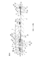
第1ベース絶縁層41と第2ベース絶縁層42と第1導体パターン21と第2導体パターン22とを備え、第1導体パターン21は、第1ベース絶縁層41の上、かつ、第2ベース絶縁層42の下に形成される素子側連絡部31と、それに連続する素子側端子25とを備え、第2導体パターン21は、第2ベース絶縁層42の上に形成されるヘッド側連絡部37と、それに連続するヘッド側端子35とを備え、2つのピエゾ素子4が、素子側端子25と電気的に接続されるように設けられており、素子側端子25は、間隔を隔てるように2対設けられており、各ピエゾ素子4を、2対の素子側端子25間に架設する。
【選択図】図3
Description
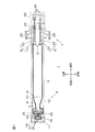
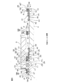
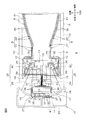
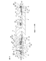
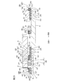
図1は、本発明の配線回路基板の第1実施形態としての回路付サスペンション基板(素子用配線供給側部分およびヘッド用配線外部側部分が第2ベース絶縁層の上に形成される態様)の平面図、図2は、図1に示す回路付サスペンション基板のジンバル部の拡大平面図、図3は、図2に示すジンバル部のA−A線に沿う断面図、図4は、図2に示すジンバル部の拡大平面図であって、カバー絶縁層が省略される平面図、図5は、図2に示すジンバル部の拡大平面図であって、第2ベース絶縁層と、その上に形成される第1導体パターンおよび第2導体パターンと、カバー絶縁層とが省略される平面図、図6および図7は、図1に示す回路付サスペンション基板の製造方法を説明するための工程図、図8は、図2に示すジンバル部のステージを揺動させた状態の平面図を示す。
(第2実施形態)
図9〜図13を参照して、回路付サスペンション基板の第2実施形態を説明する。なお、図9〜図13において、上記した第1実施形態と同様の部材については、同一の参照符号を付し、その詳細な説明を省略する。
(第3実施形態)
図14〜図16を参照して、回路付サスペンション基板の第3実施形態を説明する。なお、図14〜図16において、上記した第1実施形態と同様の部材については、同一の参照符号を付し、その詳細な説明を省略する。
(第4実施形態)
図17〜図19を参照して、回路付サスペンション基板の第4実施形態を説明する。なお、図17〜図19において、上記した第3実施形態と同様の部材については、同一の参照符号を付し、その詳細な説明を省略する。
(第5実施形態)
図20〜図22を参照して、回路付サスペンション基板の第5実施形態を説明する。なお、図20〜図22において、上記した第4実施形態と同様の部材については、同一の参照符号を付し、その詳細な説明を省略する。
(第6実施形態)
図21〜図23を参照して、回路付サスペンション基板の第6実施形態を説明する。なお、図21〜図23において、上記した第1実施形態と同様の部材については、同一の参照符号を付し、その詳細な説明を省略する。
(その他の変形例)
なお、上記した第1実施形態では、第1ベース絶縁層41を、本体部7およびジンバル部8にわたって設けているが、例えば、図5の仮想線で示すように、ジンバル部8における素子側連絡部31のみに対応するように、素子側連絡部31の下に形成することもできる。
2 磁気ヘッド
3 スライダ
4 ピエゾ素子(電子素子)
5 金属支持基板
6 導体層
16 第2基板開口部
21 第1導体パターン
22 第2導体パターン
25 素子側端子(第1端子)
31 素子側連絡部(第1連絡部)
32 素子用配線供給側部分(第1配線)
35 ヘッド側端子(第2端子)
37 ヘッド側連絡部(第2連絡部)
38 ヘッド用配線外部側部分(第2配線)
41 第1ベース絶縁層(第1絶縁層)
42 第2ベース絶縁層(第2絶縁層)
Claims (7)
- 絶縁層と、前記絶縁層の上に形成される導体層とを備える配線回路基板であり、
前記絶縁層は、第1絶縁層と、前記第1絶縁層の上に形成される第2絶縁層とを備え、前記導体層は、第1導体パターンと、第2導体パターンとを備え、
前記第1導体パターンは、
第1絶縁層の上、かつ、前記第2絶縁層の下に形成される第1連絡部と、
前記第1連絡部に連続して、外部の電子素子に対して電気的に接続されるように構成され、前記電子素子が架設されるように互いに間隔を隔てて設けられる少なくとも1対の第1端子と
を備え、
前記第2導体パターンは、
前記第2絶縁層の上に形成される第2連絡部と、
前記第2連絡部に連続して、外部のスライダに設けられる磁気ヘッドに電気的に接続されるように構成される第2端子と
を備えていることを特徴とする、配線回路基板。 - 前記第1導体パターンは、前記第1連絡部と電気的に接続される第1配線を備え、
前記第2導体パターンは、前記第2連絡部と電気的に接続される第2配線を備え、
前記第1配線および前記第2配線は、前記第2絶縁層の上に形成されていることを特徴とする、請求項1に記載の配線回路基板。 - 前記第1導体パターンは、前記第1連絡部と電気的に接続される第1配線を備え、
前記第2導体パターンは、前記第2連絡部と電気的に接続される第2配線を備え、
前記第1配線および前記第2配線は、前記第1絶縁層の上に形成されていることを特徴とする、請求項1に記載の配線回路基板。 - 前記第1絶縁層の下に形成される金属支持基板を備え、
前記金属支持基板には、内側に前記電子素子が配置されるように、厚み方向を貫通する開口部が形成されていることを特徴とする、請求項1〜3のいずれか一項に記載の配線回路基板。 - 前記開口部は、前記スライダの少なくとも一部と厚み方向に重複するように、形成されていることを特徴とする、請求項4に記載の配線回路基板。
- 前記電子素子が、ピエゾ素子であることを特徴とする、請求項1〜5のいずれか一項に記載の配線回路基板。
- 回路付サスペンション基板として用いられることを特徴とする、請求項1〜6のいずれか一項に記載の配線回路基板。
Priority Applications (1)
| Application Number | Priority Date | Filing Date | Title |
|---|---|---|---|
| JP2012151723A JP5896845B2 (ja) | 2011-08-22 | 2012-07-05 | 配線回路基板 |
Applications Claiming Priority (3)
| Application Number | Priority Date | Filing Date | Title |
|---|---|---|---|
| JP2011180971 | 2011-08-22 | ||
| JP2011180971 | 2011-08-22 | ||
| JP2012151723A JP5896845B2 (ja) | 2011-08-22 | 2012-07-05 | 配線回路基板 |
Publications (2)
| Publication Number | Publication Date |
|---|---|
| JP2013062012A true JP2013062012A (ja) | 2013-04-04 |
| JP5896845B2 JP5896845B2 (ja) | 2016-03-30 |
Family
ID=47534424
Family Applications (1)
| Application Number | Title | Priority Date | Filing Date |
|---|---|---|---|
| JP2012151723A Active JP5896845B2 (ja) | 2011-08-22 | 2012-07-05 | 配線回路基板 |
Country Status (3)
| Country | Link |
|---|---|
| US (1) | US8809691B2 (ja) |
| JP (1) | JP5896845B2 (ja) |
| CN (1) | CN102890938B (ja) |
Cited By (8)
| Publication number | Priority date | Publication date | Assignee | Title |
|---|---|---|---|---|
| JP2015076107A (ja) * | 2013-10-07 | 2015-04-20 | 大日本印刷株式会社 | サスペンション用基板、サスペンション、ヘッド付サスペンションおよびハードディスクドライブ |
| JP2015082328A (ja) * | 2013-10-21 | 2015-04-27 | 大日本印刷株式会社 | サスペンション用基板、サスペンション、ヘッド付サスペンションおよびハードディスクドライブ |
| US9147412B2 (en) | 2013-12-25 | 2015-09-29 | Nitto Denko Corporation | Head gimbal assembly |
| JP2016018570A (ja) * | 2014-07-07 | 2016-02-01 | 日東電工株式会社 | 回路付サスペンション基板 |
| US9693467B2 (en) | 2013-12-04 | 2017-06-27 | Nitto Denko Corporation | Producing method of suspension board with circuit |
| JP2018041521A (ja) * | 2016-09-07 | 2018-03-15 | 日東電工株式会社 | 回路付サスペンション基板および回路付サスペンション基板の製造方法 |
| JP2018041520A (ja) * | 2016-09-07 | 2018-03-15 | 日東電工株式会社 | 回路付サスペンション基板および回路付サスペンション基板の製造方法 |
| JP2022079213A (ja) * | 2020-11-16 | 2022-05-26 | 株式会社東芝 | サスペンションアッセンブリおよびディスク装置 |
Families Citing this family (23)
| Publication number | Priority date | Publication date | Assignee | Title |
|---|---|---|---|---|
| US8885299B1 (en) | 2010-05-24 | 2014-11-11 | Hutchinson Technology Incorporated | Low resistance ground joints for dual stage actuation disk drive suspensions |
| JP6251745B2 (ja) * | 2012-09-14 | 2017-12-20 | ハッチンソン テクノロジー インコーポレイテッドHutchinson Technology Incorporated | 2段始動構造部を有するジンバル形撓み部材及びサスペンション |
| WO2014059128A2 (en) | 2012-10-10 | 2014-04-17 | Hutchinson Technology Incorporated | Co-located gimbal-based dual stage actuation disk drive suspensions with dampers |
| US8891206B2 (en) | 2012-12-17 | 2014-11-18 | Hutchinson Technology Incorporated | Co-located gimbal-based dual stage actuation disk drive suspensions with motor stiffener |
| US8982513B1 (en) * | 2013-05-21 | 2015-03-17 | Western Digital Technologies, Inc. | Disk drive head suspension with dual piezoelectric elements adhered to rotary-actuated and non-actuated portions of a structural layer of a tongue of a laminated flexure |
| US8896969B1 (en) | 2013-05-23 | 2014-11-25 | Hutchinson Technology Incorporated | Two-motor co-located gimbal-based dual stage actuation disk drive suspensions with motor stiffeners |
| JP6169894B2 (ja) * | 2013-05-28 | 2017-07-26 | 日東電工株式会社 | 配線回路基板 |
| US8717712B1 (en) | 2013-07-15 | 2014-05-06 | Hutchinson Technology Incorporated | Disk drive suspension assembly having a partially flangeless load point dimple |
| JP6157968B2 (ja) * | 2013-07-25 | 2017-07-05 | 日東電工株式会社 | 配線回路基板およびその製造方法 |
| US8675314B1 (en) | 2013-08-21 | 2014-03-18 | Hutchinson Technology Incorporated | Co-located gimbal-based dual stage actuation disk drive suspensions with offset motors |
| KR101416159B1 (ko) * | 2013-09-06 | 2014-07-14 | 주식회사 기가레인 | 접촉 패드를 구비하는 인쇄회로기판 |
| US8896970B1 (en) | 2013-12-31 | 2014-11-25 | Hutchinson Technology Incorporated | Balanced co-located gimbal-based dual stage actuation disk drive suspensions |
| JP6370619B2 (ja) * | 2014-06-26 | 2018-08-08 | 日東電工株式会社 | 回路付サスペンション基板およびその製造方法 |
| JP6370666B2 (ja) * | 2014-10-15 | 2018-08-08 | 日東電工株式会社 | 回路付サスペンション基板 |
| US9070392B1 (en) * | 2014-12-16 | 2015-06-30 | Hutchinson Technology Incorporated | Piezoelectric disk drive suspension motors having plated stiffeners |
| US9318136B1 (en) * | 2014-12-22 | 2016-04-19 | Hutchinson Technology Incorporated | Multilayer disk drive motors having out-of-plane bending |
| US9296188B1 (en) | 2015-02-17 | 2016-03-29 | Hutchinson Technology Incorporated | Partial curing of a microactuator mounting adhesive in a disk drive suspension |
| JP6466747B2 (ja) * | 2015-03-12 | 2019-02-06 | 日東電工株式会社 | 回路付サスペンション基板およびその製造方法 |
| CN107735834B (zh) | 2015-06-30 | 2019-11-19 | 哈钦森技术股份有限公司 | 具有改进的可靠性的盘驱动器头部悬架结构 |
| JP2017021878A (ja) | 2015-07-13 | 2017-01-26 | 日東電工株式会社 | 回路付きサスペンション基板集合体シート、その製造方法およびその検査方法 |
| JP6646425B2 (ja) * | 2015-12-11 | 2020-02-14 | 日東電工株式会社 | 回路付サスペンション基板およびその製造方法 |
| US9646638B1 (en) | 2016-05-12 | 2017-05-09 | Hutchinson Technology Incorporated | Co-located gimbal-based DSA disk drive suspension with traces routed around slider pad |
| JP7004212B2 (ja) * | 2018-02-13 | 2022-01-21 | 住友電装株式会社 | 回路構成体及び電気接続箱 |
Citations (7)
| Publication number | Priority date | Publication date | Assignee | Title |
|---|---|---|---|---|
| JPH0922570A (ja) * | 1995-07-03 | 1997-01-21 | Fujitsu Ltd | ヘッドアセンブリ及び該ヘッドアセンブリを具備した磁気ディスク装置 |
| JPH103632A (ja) * | 1996-06-12 | 1998-01-06 | Dainippon Printing Co Ltd | 磁気ヘッドサスペンション |
| JP2009129490A (ja) * | 2007-11-21 | 2009-06-11 | Nitto Denko Corp | 配線回路基板 |
| JP2010108576A (ja) * | 2008-10-31 | 2010-05-13 | Nitto Denko Corp | 回路付サスペンション基板 |
| JP2010146631A (ja) * | 2008-12-18 | 2010-07-01 | Hitachi Global Storage Technologies Netherlands Bv | ヘッド・ジンバル・アセンブリ及びディスク・ドライブ |
| JP2010218626A (ja) * | 2009-03-17 | 2010-09-30 | Hitachi Global Storage Technologies Netherlands Bv | ヘッド・ジンバル・アセンブリ及びディスク・ドライブ |
| JP2011082302A (ja) * | 2009-10-06 | 2011-04-21 | Dainippon Printing Co Ltd | 配線回路基板、サスペンション、ヘッド付サスペンション、ハードディスクドライブおよび配線回路基板の製造方法 |
Family Cites Families (4)
| Publication number | Priority date | Publication date | Assignee | Title |
|---|---|---|---|---|
| JP3891912B2 (ja) * | 2002-10-09 | 2007-03-14 | 日本発条株式会社 | ディスクドライブ用サスペンション |
| JP4845227B2 (ja) | 2007-06-29 | 2011-12-28 | 東芝ストレージデバイス株式会社 | ヘッドサスペンションアセンブリおよび記憶媒体駆動装置 |
| JP2009246092A (ja) * | 2008-03-31 | 2009-10-22 | Nitto Denko Corp | 配線回路基板およびその製造方法 |
| JP5002574B2 (ja) * | 2008-11-11 | 2012-08-15 | 日東電工株式会社 | 回路付サスペンション基板およびその製造方法 |
-
2012
- 2012-07-05 JP JP2012151723A patent/JP5896845B2/ja active Active
- 2012-07-19 CN CN201210252194.5A patent/CN102890938B/zh not_active Expired - Fee Related
- 2012-07-20 US US13/554,799 patent/US8809691B2/en not_active Expired - Fee Related
Patent Citations (7)
| Publication number | Priority date | Publication date | Assignee | Title |
|---|---|---|---|---|
| JPH0922570A (ja) * | 1995-07-03 | 1997-01-21 | Fujitsu Ltd | ヘッドアセンブリ及び該ヘッドアセンブリを具備した磁気ディスク装置 |
| JPH103632A (ja) * | 1996-06-12 | 1998-01-06 | Dainippon Printing Co Ltd | 磁気ヘッドサスペンション |
| JP2009129490A (ja) * | 2007-11-21 | 2009-06-11 | Nitto Denko Corp | 配線回路基板 |
| JP2010108576A (ja) * | 2008-10-31 | 2010-05-13 | Nitto Denko Corp | 回路付サスペンション基板 |
| JP2010146631A (ja) * | 2008-12-18 | 2010-07-01 | Hitachi Global Storage Technologies Netherlands Bv | ヘッド・ジンバル・アセンブリ及びディスク・ドライブ |
| JP2010218626A (ja) * | 2009-03-17 | 2010-09-30 | Hitachi Global Storage Technologies Netherlands Bv | ヘッド・ジンバル・アセンブリ及びディスク・ドライブ |
| JP2011082302A (ja) * | 2009-10-06 | 2011-04-21 | Dainippon Printing Co Ltd | 配線回路基板、サスペンション、ヘッド付サスペンション、ハードディスクドライブおよび配線回路基板の製造方法 |
Cited By (9)
| Publication number | Priority date | Publication date | Assignee | Title |
|---|---|---|---|---|
| JP2015076107A (ja) * | 2013-10-07 | 2015-04-20 | 大日本印刷株式会社 | サスペンション用基板、サスペンション、ヘッド付サスペンションおよびハードディスクドライブ |
| JP2015082328A (ja) * | 2013-10-21 | 2015-04-27 | 大日本印刷株式会社 | サスペンション用基板、サスペンション、ヘッド付サスペンションおよびハードディスクドライブ |
| US9693467B2 (en) | 2013-12-04 | 2017-06-27 | Nitto Denko Corporation | Producing method of suspension board with circuit |
| US9147412B2 (en) | 2013-12-25 | 2015-09-29 | Nitto Denko Corporation | Head gimbal assembly |
| JP2016018570A (ja) * | 2014-07-07 | 2016-02-01 | 日東電工株式会社 | 回路付サスペンション基板 |
| JP2018041521A (ja) * | 2016-09-07 | 2018-03-15 | 日東電工株式会社 | 回路付サスペンション基板および回路付サスペンション基板の製造方法 |
| JP2018041520A (ja) * | 2016-09-07 | 2018-03-15 | 日東電工株式会社 | 回路付サスペンション基板および回路付サスペンション基板の製造方法 |
| JP2022079213A (ja) * | 2020-11-16 | 2022-05-26 | 株式会社東芝 | サスペンションアッセンブリおよびディスク装置 |
| JP7413237B2 (ja) | 2020-11-16 | 2024-01-15 | 株式会社東芝 | サスペンションアッセンブリおよびディスク装置 |
Also Published As
| Publication number | Publication date |
|---|---|
| CN102890938B (zh) | 2016-12-21 |
| US8809691B2 (en) | 2014-08-19 |
| JP5896845B2 (ja) | 2016-03-30 |
| US20130020112A1 (en) | 2013-01-24 |
| CN102890938A (zh) | 2013-01-23 |
Similar Documents
| Publication | Publication Date | Title |
|---|---|---|
| JP5896845B2 (ja) | 配線回路基板 | |
| JP6029813B2 (ja) | 回路付サスペンション基板 | |
| JP5896846B2 (ja) | 回路付サスペンション基板 | |
| JP6043613B2 (ja) | 回路付サスペンション基板 | |
| JP5989370B2 (ja) | 配線回路基板 | |
| US8854826B2 (en) | Suspension board with circuit | |
| JP5801085B2 (ja) | 回路付サスペンション基板 | |
| US8593823B2 (en) | Suspension board with circuit | |
| US20130014976A1 (en) | Wired circuit board and producing method thereof | |
| US9253879B2 (en) | Wired circuit board and producing method thereof | |
| JP2016081542A (ja) | 回路付サスペンション基板 | |
| US9992868B2 (en) | Wired circuit board having one of the conductive layers disposed in an opening formed in metal supporting board | |
| JP2017107628A (ja) | 回路付サスペンション基板およびその製造方法 | |
| JP6280828B2 (ja) | 回路付サスペンション基板 | |
| JP6539194B2 (ja) | 回路付サスペンション基板およびその製造方法 | |
| JP2015207330A (ja) | 回路付サスペンション基板 | |
| US20180358037A1 (en) | Suspension board with circuits | |
| US20180358040A1 (en) | Suspension board with circuits | |
| JP6818169B2 (ja) | 回路付サスペンション基板 | |
| JP2013137846A (ja) | 回路付サスペンション基板 |
Legal Events
| Date | Code | Title | Description |
|---|---|---|---|
| A621 | Written request for application examination |
Free format text: JAPANESE INTERMEDIATE CODE: A621 Effective date: 20150424 |
|
| A977 | Report on retrieval |
Free format text: JAPANESE INTERMEDIATE CODE: A971007 Effective date: 20151214 |
|
| TRDD | Decision of grant or rejection written | ||
| A01 | Written decision to grant a patent or to grant a registration (utility model) |
Free format text: JAPANESE INTERMEDIATE CODE: A01 Effective date: 20160209 |
|
| A61 | First payment of annual fees (during grant procedure) |
Free format text: JAPANESE INTERMEDIATE CODE: A61 Effective date: 20160301 |
|
| R150 | Certificate of patent or registration of utility model |
Ref document number: 5896845 Country of ref document: JP Free format text: JAPANESE INTERMEDIATE CODE: R150 |
|
| R250 | Receipt of annual fees |
Free format text: JAPANESE INTERMEDIATE CODE: R250 |
|
| R250 | Receipt of annual fees |
Free format text: JAPANESE INTERMEDIATE CODE: R250 |
|
| R250 | Receipt of annual fees |
Free format text: JAPANESE INTERMEDIATE CODE: R250 |
|
| R250 | Receipt of annual fees |
Free format text: JAPANESE INTERMEDIATE CODE: R250 |
|
| R250 | Receipt of annual fees |
Free format text: JAPANESE INTERMEDIATE CODE: R250 |
|
| R250 | Receipt of annual fees |
Free format text: JAPANESE INTERMEDIATE CODE: R250 |
|
| R250 | Receipt of annual fees |
Free format text: JAPANESE INTERMEDIATE CODE: R250 |
|
| R250 | Receipt of annual fees |
Free format text: JAPANESE INTERMEDIATE CODE: R250 |