JP2013065009A - タッチ・ディスプレイ装置及び製造方法 - Google Patents
タッチ・ディスプレイ装置及び製造方法 Download PDFInfo
- Publication number
- JP2013065009A JP2013065009A JP2012192809A JP2012192809A JP2013065009A JP 2013065009 A JP2013065009 A JP 2013065009A JP 2012192809 A JP2012192809 A JP 2012192809A JP 2012192809 A JP2012192809 A JP 2012192809A JP 2013065009 A JP2013065009 A JP 2013065009A
- Authority
- JP
- Japan
- Prior art keywords
- adhesive
- touch
- curable liquid
- display device
- induced
- Prior art date
- Legal status (The legal status is an assumption and is not a legal conclusion. Google has not performed a legal analysis and makes no representation as to the accuracy of the status listed.)
- Granted
Links
Images

Classifications
-
- G—PHYSICS
- G06—COMPUTING OR CALCULATING; COUNTING
- G06F—ELECTRIC DIGITAL DATA PROCESSING
- G06F3/00—Input arrangements for transferring data to be processed into a form capable of being handled by the computer; Output arrangements for transferring data from processing unit to output unit, e.g. interface arrangements
- G06F3/01—Input arrangements or combined input and output arrangements for interaction between user and computer
- G06F3/03—Arrangements for converting the position or the displacement of a member into a coded form
- G06F3/041—Digitisers, e.g. for touch screens or touch pads, characterised by the transducing means
-
- G—PHYSICS
- G06—COMPUTING OR CALCULATING; COUNTING
- G06F—ELECTRIC DIGITAL DATA PROCESSING
- G06F3/00—Input arrangements for transferring data to be processed into a form capable of being handled by the computer; Output arrangements for transferring data from processing unit to output unit, e.g. interface arrangements
- G06F3/01—Input arrangements or combined input and output arrangements for interaction between user and computer
- G06F3/03—Arrangements for converting the position or the displacement of a member into a coded form
- G06F3/041—Digitisers, e.g. for touch screens or touch pads, characterised by the transducing means
- G06F3/0412—Digitisers structurally integrated in a display
-
- B—PERFORMING OPERATIONS; TRANSPORTING
- B32—LAYERED PRODUCTS
- B32B—LAYERED PRODUCTS, i.e. PRODUCTS BUILT-UP OF STRATA OF FLAT OR NON-FLAT, e.g. CELLULAR OR HONEYCOMB, FORM
- B32B7/00—Layered products characterised by the relation between layers; Layered products characterised by the relative orientation of features between layers, or by the relative values of a measurable parameter between layers, i.e. products comprising layers having different physical, chemical or physicochemical properties; Layered products characterised by the interconnection of layers
- B32B7/04—Interconnection of layers
- B32B7/12—Interconnection of layers using interposed adhesives or interposed materials with bonding properties
-
- G—PHYSICS
- G09—EDUCATION; CRYPTOGRAPHY; DISPLAY; ADVERTISING; SEALS
- G09F—DISPLAYING; ADVERTISING; SIGNS; LABELS OR NAME-PLATES; SEALS
- G09F9/00—Indicating arrangements for variable information in which the information is built-up on a support by selection or combination of individual elements
-
- H—ELECTRICITY
- H05—ELECTRIC TECHNIQUES NOT OTHERWISE PROVIDED FOR
- H05K—PRINTED CIRCUITS; CASINGS OR CONSTRUCTIONAL DETAILS OF ELECTRIC APPARATUS; MANUFACTURE OF ASSEMBLAGES OF ELECTRICAL COMPONENTS
- H05K1/00—Printed circuits
- H05K1/02—Details
- H05K1/11—Printed elements for providing electric connections to or between printed circuits
- H05K1/118—Printed elements for providing electric connections to or between printed circuits specially for flexible printed circuits, e.g. using folded portions
-
- G—PHYSICS
- G06—COMPUTING OR CALCULATING; COUNTING
- G06F—ELECTRIC DIGITAL DATA PROCESSING
- G06F2203/00—Indexing scheme relating to G06F3/00 - G06F3/048
- G06F2203/041—Indexing scheme relating to G06F3/041 - G06F3/045
- G06F2203/04102—Flexible digitiser, i.e. constructional details for allowing the whole digitising part of a device to be flexed or rolled like a sheet of paper
-
- G—PHYSICS
- G06—COMPUTING OR CALCULATING; COUNTING
- G06F—ELECTRIC DIGITAL DATA PROCESSING
- G06F2203/00—Indexing scheme relating to G06F3/00 - G06F3/048
- G06F2203/041—Indexing scheme relating to G06F3/041 - G06F3/045
- G06F2203/04103—Manufacturing, i.e. details related to manufacturing processes specially suited for touch sensitive devices
-
- Y—GENERAL TAGGING OF NEW TECHNOLOGICAL DEVELOPMENTS; GENERAL TAGGING OF CROSS-SECTIONAL TECHNOLOGIES SPANNING OVER SEVERAL SECTIONS OF THE IPC; TECHNICAL SUBJECTS COVERED BY FORMER USPC CROSS-REFERENCE ART COLLECTIONS [XRACs] AND DIGESTS
- Y10—TECHNICAL SUBJECTS COVERED BY FORMER USPC
- Y10T—TECHNICAL SUBJECTS COVERED BY FORMER US CLASSIFICATION
- Y10T156/00—Adhesive bonding and miscellaneous chemical manufacture
- Y10T156/10—Methods of surface bonding and/or assembly therefor
Landscapes
- Engineering & Computer Science (AREA)
- Theoretical Computer Science (AREA)
- General Engineering & Computer Science (AREA)
- Physics & Mathematics (AREA)
- General Physics & Mathematics (AREA)
- Human Computer Interaction (AREA)
- Microelectronics & Electronic Packaging (AREA)
- Position Input By Displaying (AREA)
- Devices For Indicating Variable Information By Combining Individual Elements (AREA)
- Adhesives Or Adhesive Processes (AREA)
- Lining Or Joining Of Plastics Or The Like (AREA)
Abstract
【解決手段】タッチ・ディスプレイ装置とその製造方法を提供する。タッチ・ディスプレイ装置は、タッチパネル、ディスプレイモジュール、紫外線硬化液体接着剤により形成され、タッチパネルとディスプレイモジュールを貼合する第1の接着層を有する。該タッチ・ディスプレイ装置は、さらに、レンズと第2の接着層を有し、該第2の接着層は、レンズとタッチ基板を貼合する。本発明にかかる技術は、ディスプレイモジュール、タッチ基板、レンズの貼合順を調整することにより、第1の接着層と第2の接着層の硬化による遮光影響を克服し、タッチパネルとディスプレイモジュール間の貼合を強くする。
【選択図】図1
Description
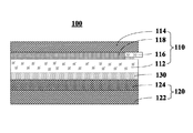
110 タッチパネル
112 タッチ基板
114 レンズ
116 フレキシブルプリント基板
118 第2の接着層
120 ディスプレイモジュール
122 ディスプレイパネル
124 ディフューザー
130 第1の接着層
Claims (13)
- 第1の接着剤により、ディスプレイモジュールをタッチ基板に貼合するステップ(a)と、
第2の接着剤により、レンズを前記ディスプレイモジュールの表面に貼合するステップ(b)とを有する、
タッチ・ディスプレイ装置の製造方法。 - 前記第1の接着剤及び/または前記第2の接着剤は、光硬化液体接着剤である、
請求項1に記載のタッチ・ディスプレイ装置の製造方法。 - 前記光硬化液体接着剤は、紫外線硬化液体接着剤と、熱誘発紫外線硬化液体接着剤と、水分誘発紫外線硬化液体接着剤と、これらの組合せから選択されたものである、
請求項2に記載のタッチ・ディスプレイ装置の製造方法。 - 前記ステップ(a)と前記ステップ(b)の間に、前記第1の接着剤に対して光硬化処理を施し、第1の接着層を形成するステップ(c)をさらに有する、
請求項1から3のいずれか1項に記載のタッチ・ディスプレイ装置の製造方法。 - 前記ステップ(b)の後に、前記第2の接着剤に対して光硬化処理を施し、第2の接着層を形成するステップ(d)をさらに有する、
請求項1から4のいずれか1項に記載のタッチ・ディスプレイ装置の製造方法。 - 前記第1の接着剤と前記第2の接着剤が熱誘発紫外線硬化液体接着剤であり、
前記光硬化処理は、さらに、
紫外線光により前記熱誘発紫外線硬化液体接着剤の光硬化を施し、
加熱工程により、前記熱誘発紫外線硬化液体接着剤の硬化を強化する処理を含む、
請求項4または5に記載のタッチ・ディスプレイ装置の製造方法。 - 前記第1の接着剤と前記第2の接着剤が水分誘発紫外線硬化液体接着剤であり、
前記光硬化処理は、さらに、
紫外線光により前記水分誘発紫外線硬化液体接着剤の光硬化を施し、
水分により、前記水分誘発紫外線硬化液体接着剤の硬化を強化する処理を含む、
請求項4または5に記載のタッチ・ディスプレイ装置の製造方法。 - フレキシブルプリント基板を前記タッチ基板に貼合するステップをさらに有する、
請求項1から7のいずれか1項に記載のタッチ・ディスプレイ装置の製造方法。 - タッチ基板と、
第1の接着層により前記タッチ基板に貼合されたディスプレイモジュールと、
第2の接着層により前記タッチ基板の表面に貼合されたレンズとを備える、
タッチ・ディスプレイ装置。 - 前記第1の接着層と前記第2の接着層は、紫外線硬化液体接着剤と、熱誘発紫外線硬化液体接着剤と、水分誘発紫外線硬化液体接着剤と、これらの組合せから選択されたものにより形成されている、
請求項9に記載のタッチ・ディスプレイ装置。 - 前記第1の接着層及び/または前記第2の接着層は、アクリルまたはシリコンベースの製品である、
請求項10に記載のタッチ・ディスプレイ装置。 - 前記レンズの回りに、不透光層が形成されている、
請求項9から11のいずれか1項に記載のタッチ・ディスプレイ装置。 - 前記タッチ基板上に、
タッチ感知層と、
前記タッチ感知層と電気的に接続された周辺回路層とが形成されている、
請求項9から12のいずれか1項に記載のタッチ・ディスプレイ装置。
Applications Claiming Priority (2)
| Application Number | Priority Date | Filing Date | Title |
|---|---|---|---|
| CN201110289572.2 | 2011-09-18 | ||
| CN2011102895722A CN102999200A (zh) | 2011-09-18 | 2011-09-18 | 触控显示装置及其制造方法 |
Publications (2)
| Publication Number | Publication Date |
|---|---|
| JP2013065009A true JP2013065009A (ja) | 2013-04-11 |
| JP5686777B2 JP5686777B2 (ja) | 2015-03-18 |
Family
ID=47178456
Family Applications (1)
| Application Number | Title | Priority Date | Filing Date |
|---|---|---|---|
| JP2012192809A Expired - Fee Related JP5686777B2 (ja) | 2011-09-18 | 2012-09-03 | タッチ・ディスプレイ装置及び製造方法 |
Country Status (6)
| Country | Link |
|---|---|
| US (1) | US20130069890A1 (ja) |
| EP (1) | EP2570899B1 (ja) |
| JP (1) | JP5686777B2 (ja) |
| KR (1) | KR101452954B1 (ja) |
| CN (1) | CN102999200A (ja) |
| TW (2) | TWI581133B (ja) |
Cited By (14)
| Publication number | Priority date | Publication date | Assignee | Title |
|---|---|---|---|---|
| JPWO2015033610A1 (ja) * | 2013-09-09 | 2017-03-02 | 日本化薬株式会社 | 光学部材の製造方法及びそれに用いる紫外線硬化型樹脂組成物 |
| WO2017183541A1 (ja) | 2016-04-22 | 2017-10-26 | 東レ・ダウコーニング株式会社 | 高誘電性フィルム、その用途および製造方法 |
| WO2018186161A1 (ja) | 2017-04-03 | 2018-10-11 | 東レ・ダウコーニング株式会社 | 硬化反応性のオルガノポリシロキサン組成物、それを用いた感圧接着剤組成物、およびその使用 |
| WO2019009175A1 (ja) | 2017-07-07 | 2019-01-10 | 東レ・ダウコーニング株式会社 | 感圧接着層形成性オルガノポリシロキサン組成物およびその使用 |
| US10357947B2 (en) | 2015-04-10 | 2019-07-23 | Dow Toray Co., Ltd. | Fluoroalkyl-containing curable organopolysiloxane composition, cured object obtained therefrom, and electronic component or display device including said cured object |
| WO2020032285A1 (ja) | 2018-08-10 | 2020-02-13 | ダウ・東レ株式会社 | 感圧接着層形成性オルガノポリシロキサン組成物およびその使用 |
| WO2020032286A1 (ja) | 2018-08-10 | 2020-02-13 | ダウ・東レ株式会社 | 感圧接着層形成性オルガノポリシロキサン組成物およびその使用 |
| WO2020032287A1 (ja) | 2018-08-10 | 2020-02-13 | ダウ・東レ株式会社 | 感圧接着層形成性オルガノポリシロキサン組成物およびその使用 |
| WO2020090797A1 (ja) | 2018-10-30 | 2020-05-07 | ダウ・東レ株式会社 | 硬化反応性シリコーン組成物及びその硬化物並びにそれらの用途 |
| WO2020121930A1 (ja) | 2018-12-13 | 2020-06-18 | ダウ・東レ株式会社 | シリコーン粘着剤組成物およびその用途 |
| WO2021029412A1 (ja) | 2019-08-13 | 2021-02-18 | ダウ・東レ株式会社 | 感圧接着層形成性オルガノポリシロキサン組成物およびその使用 |
| WO2021029414A1 (ja) | 2019-08-13 | 2021-02-18 | ダウ・東レ株式会社 | 感圧接着層形成性オルガノポリシロキサン組成物およびその使用 |
| WO2021029413A1 (ja) | 2019-08-13 | 2021-02-18 | ダウ・東レ株式会社 | 感圧接着層形成性オルガノポリシロキサン組成物およびその使用 |
| WO2022138345A1 (ja) | 2020-12-25 | 2022-06-30 | ダウ・東レ株式会社 | シリコーン粘着剤組成物およびその用途 |
Families Citing this family (13)
| Publication number | Priority date | Publication date | Assignee | Title |
|---|---|---|---|---|
| US20150062448A1 (en) * | 2013-08-30 | 2015-03-05 | Arvind S. | Touch screen displays |
| TW201512915A (zh) * | 2013-09-18 | 2015-04-01 | Silitech Technology Corp | 觸控面板 |
| CN104635963B (zh) * | 2013-11-07 | 2018-02-23 | 群创光电股份有限公司 | 触控显示装置与其制造方法 |
| US20160329562A1 (en) | 2014-12-16 | 2016-11-10 | Sanyo Electric Co., Ltd. | Negative electrode active material for nonaqueous electrolyte secondary batteries and nonaqueous electrolyte secondary battery containing negative electrode active material |
| CN105204686B (zh) * | 2015-09-23 | 2019-05-31 | 联想(北京)有限公司 | 一种电子设备 |
| US20170108959A1 (en) * | 2015-10-15 | 2017-04-20 | Richard Keith McMillan | Two piece lens assembly |
| CN105468199B (zh) * | 2015-12-26 | 2019-01-15 | 宸鸿科技(厦门)有限公司 | 一种具有压力感测的面板 |
| CN106873827B (zh) * | 2017-01-16 | 2020-04-17 | 业成科技(成都)有限公司 | 触控偏光单元、可挠性触控显示设备以及可挠性触控显示设备的制造方法 |
| CN110413154A (zh) * | 2019-07-25 | 2019-11-05 | 深圳市华星光电半导体显示技术有限公司 | 触控显示装置及其制造方法 |
| CN113359339A (zh) * | 2020-03-06 | 2021-09-07 | 北京小米移动软件有限公司 | 显示屏、显示屏防水处理工艺和终端设备 |
| CN111524939A (zh) * | 2020-04-26 | 2020-08-11 | 武汉华星光电半导体显示技术有限公司 | 柔性显示面板及其组装方法 |
| KR20220072927A (ko) * | 2020-11-25 | 2022-06-03 | 삼성디스플레이 주식회사 | 표시 장치 및 그 제조 방법 |
| TWI767665B (zh) * | 2021-04-22 | 2022-06-11 | 群光電子股份有限公司 | 觸控板裝置及其製造方法 |
Citations (3)
| Publication number | Priority date | Publication date | Assignee | Title |
|---|---|---|---|---|
| JP2008083491A (ja) * | 2006-09-28 | 2008-04-10 | Epson Imaging Devices Corp | 電気光学装置及び電子機器 |
| JP2010122563A (ja) * | 2008-11-21 | 2010-06-03 | Hitachi Displays Ltd | 表示装置及びその製造方法 |
| JP2010197692A (ja) * | 2009-02-25 | 2010-09-09 | Sekisui Chem Co Ltd | 光学部材用光硬化性樹脂組成物、接着剤、及び、タッチパネル |
Family Cites Families (14)
| Publication number | Priority date | Publication date | Assignee | Title |
|---|---|---|---|---|
| JP2005107655A (ja) * | 2003-09-29 | 2005-04-21 | Kawaguchiko Seimitsu Co Ltd | タッチパネル及びその製造方法 |
| JP2006235571A (ja) * | 2005-01-28 | 2006-09-07 | Victor Co Of Japan Ltd | 投射型表示装置 |
| JP2009163132A (ja) * | 2008-01-09 | 2009-07-23 | Seiko Instruments Inc | 液晶表示装置の製造方法、液晶表示装置、及び電子機器 |
| JP5243811B2 (ja) * | 2008-02-14 | 2013-07-24 | セイコーインスツル株式会社 | 表示装置 |
| CN201174007Y (zh) * | 2008-03-18 | 2008-12-31 | 宸鸿光电科技股份有限公司 | 电容式触控面板 |
| US9573346B2 (en) * | 2008-05-21 | 2017-02-21 | Manufacturing Resources International, Inc. | Photoinitiated optical adhesive and method for using same |
| JP5235769B2 (ja) * | 2009-04-27 | 2013-07-10 | 株式会社ジャパンディスプレイイースト | 液晶表示装置 |
| TWI412817B (zh) * | 2009-06-02 | 2013-10-21 | Wintek Corp | 觸控顯示裝置 |
| US20110005662A1 (en) * | 2009-07-10 | 2011-01-13 | Kuo-Hua Sung | Method for Fabricating Multilayer Panels |
| KR101229419B1 (ko) * | 2009-11-12 | 2013-02-05 | (주)멜파스 | 이방 전도성 접착제를 포함하는 접촉 감지 패널 및 그 제조 방법 |
| TW201102698A (en) * | 2010-01-26 | 2011-01-16 | Mastouch Optoelectronics Technologies Co Ltd | Single-layer projected capacitive touch panel and fabricating method thereof |
| WO2011112447A2 (en) * | 2010-03-09 | 2011-09-15 | 3M Innovative Properties Company | Heat activated optically clear adhesive for bonding display panels |
| CN101973155B (zh) * | 2010-08-24 | 2013-04-10 | 深圳市中显微电子有限公司 | 电容式触摸屏基板贴合方法以及触摸屏与显示模块的贴合方法 |
| CN202422050U (zh) * | 2011-09-18 | 2012-09-05 | 宸鸿科技(厦门)有限公司 | 触控显示装置 |
-
2011
- 2011-09-18 CN CN2011102895722A patent/CN102999200A/zh active Pending
-
2012
- 2012-04-03 TW TW101111765A patent/TWI581133B/zh not_active IP Right Cessation
- 2012-04-03 TW TW101206004U patent/TWM440475U/zh not_active IP Right Cessation
- 2012-07-26 US US13/559,532 patent/US20130069890A1/en not_active Abandoned
- 2012-08-30 KR KR1020120095756A patent/KR101452954B1/ko not_active Expired - Fee Related
- 2012-09-03 JP JP2012192809A patent/JP5686777B2/ja not_active Expired - Fee Related
- 2012-09-12 EP EP12183962.5A patent/EP2570899B1/en not_active Not-in-force
Patent Citations (3)
| Publication number | Priority date | Publication date | Assignee | Title |
|---|---|---|---|---|
| JP2008083491A (ja) * | 2006-09-28 | 2008-04-10 | Epson Imaging Devices Corp | 電気光学装置及び電子機器 |
| JP2010122563A (ja) * | 2008-11-21 | 2010-06-03 | Hitachi Displays Ltd | 表示装置及びその製造方法 |
| JP2010197692A (ja) * | 2009-02-25 | 2010-09-09 | Sekisui Chem Co Ltd | 光学部材用光硬化性樹脂組成物、接着剤、及び、タッチパネル |
Cited By (20)
| Publication number | Priority date | Publication date | Assignee | Title |
|---|---|---|---|---|
| JPWO2015033610A1 (ja) * | 2013-09-09 | 2017-03-02 | 日本化薬株式会社 | 光学部材の製造方法及びそれに用いる紫外線硬化型樹脂組成物 |
| US10357947B2 (en) | 2015-04-10 | 2019-07-23 | Dow Toray Co., Ltd. | Fluoroalkyl-containing curable organopolysiloxane composition, cured object obtained therefrom, and electronic component or display device including said cured object |
| WO2017183541A1 (ja) | 2016-04-22 | 2017-10-26 | 東レ・ダウコーニング株式会社 | 高誘電性フィルム、その用途および製造方法 |
| WO2018186161A1 (ja) | 2017-04-03 | 2018-10-11 | 東レ・ダウコーニング株式会社 | 硬化反応性のオルガノポリシロキサン組成物、それを用いた感圧接着剤組成物、およびその使用 |
| WO2019009175A1 (ja) | 2017-07-07 | 2019-01-10 | 東レ・ダウコーニング株式会社 | 感圧接着層形成性オルガノポリシロキサン組成物およびその使用 |
| US11987731B2 (en) | 2018-08-10 | 2024-05-21 | Dow Toray Co., Ltd. | Organopolysiloxane composition for forming pressure sensitive adhesive layer, and use of same |
| WO2020032285A1 (ja) | 2018-08-10 | 2020-02-13 | ダウ・東レ株式会社 | 感圧接着層形成性オルガノポリシロキサン組成物およびその使用 |
| WO2020032286A1 (ja) | 2018-08-10 | 2020-02-13 | ダウ・東レ株式会社 | 感圧接着層形成性オルガノポリシロキサン組成物およびその使用 |
| WO2020032287A1 (ja) | 2018-08-10 | 2020-02-13 | ダウ・東レ株式会社 | 感圧接着層形成性オルガノポリシロキサン組成物およびその使用 |
| US12509614B2 (en) | 2018-08-10 | 2025-12-30 | Dow Toray Co., Ltd. | Organopolysiloxane composition for forming pressure sensitive adhesive layer, and use of same |
| US12173197B2 (en) | 2018-08-10 | 2024-12-24 | Dow Toray Co., Ltd. | Organopolysiloxane composition for forming pressure sensitive adhesive layer, and use of same |
| WO2020090797A1 (ja) | 2018-10-30 | 2020-05-07 | ダウ・東レ株式会社 | 硬化反応性シリコーン組成物及びその硬化物並びにそれらの用途 |
| US12129407B2 (en) | 2018-12-13 | 2024-10-29 | Dow Silicones Corporation | Silicone adhesive composition and use thereof |
| WO2020121930A1 (ja) | 2018-12-13 | 2020-06-18 | ダウ・東レ株式会社 | シリコーン粘着剤組成物およびその用途 |
| WO2021029413A1 (ja) | 2019-08-13 | 2021-02-18 | ダウ・東レ株式会社 | 感圧接着層形成性オルガノポリシロキサン組成物およびその使用 |
| WO2021029414A1 (ja) | 2019-08-13 | 2021-02-18 | ダウ・東レ株式会社 | 感圧接着層形成性オルガノポリシロキサン組成物およびその使用 |
| WO2021029412A1 (ja) | 2019-08-13 | 2021-02-18 | ダウ・東レ株式会社 | 感圧接着層形成性オルガノポリシロキサン組成物およびその使用 |
| US12503630B2 (en) | 2019-08-13 | 2025-12-23 | Dow Toray Co., Ltd. | Organopolysiloxane composition having pressure-sensitive adhesive layer formation properties, and use of said composition |
| US12503626B2 (en) | 2019-08-13 | 2025-12-23 | Dow Toray Co., Ltd. | Organopolysiloxane composition for forming pressure sensitive adhesive layer and use of same |
| WO2022138345A1 (ja) | 2020-12-25 | 2022-06-30 | ダウ・東レ株式会社 | シリコーン粘着剤組成物およびその用途 |
Also Published As
| Publication number | Publication date |
|---|---|
| KR101452954B1 (ko) | 2014-10-21 |
| EP2570899A3 (en) | 2015-06-10 |
| EP2570899A2 (en) | 2013-03-20 |
| TWI581133B (zh) | 2017-05-01 |
| JP5686777B2 (ja) | 2015-03-18 |
| TW201314522A (zh) | 2013-04-01 |
| TWM440475U (en) | 2012-11-01 |
| KR20130030721A (ko) | 2013-03-27 |
| EP2570899B1 (en) | 2017-11-08 |
| US20130069890A1 (en) | 2013-03-21 |
| CN102999200A (zh) | 2013-03-27 |
Similar Documents
| Publication | Publication Date | Title |
|---|---|---|
| JP5686777B2 (ja) | タッチ・ディスプレイ装置及び製造方法 | |
| US10209546B2 (en) | Display panel and display device, and fabrication methods thereof | |
| CN101331529B (zh) | 显示设备以及显示设备的制造方法 | |
| CN105319778B (zh) | 显示设备及其制造方法 | |
| TWI565384B (zh) | 觸控面板 | |
| CN103338606B (zh) | 电子装置、电子装置盖板的组装方法及粘接结构 | |
| TWI537780B (zh) | Workpiece fit method and touch panel | |
| JPWO2014123165A1 (ja) | 透明面材およびそれを用いた表示装置 | |
| WO2012042822A1 (ja) | フレキシブルディスプレイ及びその製造方法 | |
| JP2010186068A (ja) | 電気光学装置、電気光学装置の製造方法および電子機器 | |
| JP2013131099A (ja) | 静電容量型タッチパネル | |
| JP2014013266A (ja) | 表示装置及びその製造方法 | |
| US9746599B2 (en) | Display device and method of fabricating the same | |
| KR101486118B1 (ko) | 점착제층을 포함하는 적층체 및 그 제조 방법 | |
| CN212312931U (zh) | 装饰膜、具备其的窗膜和窗口层压体 | |
| JP6664229B2 (ja) | 導光ブロックを有する表示装置 | |
| CN202422050U (zh) | 触控显示装置 | |
| JP2015036897A (ja) | タッチパネルの製造方法 | |
| CN201159888Y (zh) | 全平面触控面板 | |
| CN104021731A (zh) | 显示装置 | |
| WO2020143406A1 (zh) | 显示面板的制备方法、显示面板及显示装置 | |
| JP2015207058A (ja) | タッチパネルの製造方法及びタッチパネル | |
| CN203930736U (zh) | 触控显示装置 | |
| JP2022528242A (ja) | デコフィルム、これを有するウィンドウフィルムと積層体、及びその製造方法 | |
| JP2013142986A (ja) | タッチパネル部材の製造方法 |
Legal Events
| Date | Code | Title | Description |
|---|---|---|---|
| A977 | Report on retrieval |
Free format text: JAPANESE INTERMEDIATE CODE: A971007 Effective date: 20130814 |
|
| A131 | Notification of reasons for refusal |
Free format text: JAPANESE INTERMEDIATE CODE: A131 Effective date: 20130820 |
|
| A601 | Written request for extension of time |
Free format text: JAPANESE INTERMEDIATE CODE: A601 Effective date: 20131114 |
|
| A602 | Written permission of extension of time |
Free format text: JAPANESE INTERMEDIATE CODE: A602 Effective date: 20131119 |
|
| A601 | Written request for extension of time |
Free format text: JAPANESE INTERMEDIATE CODE: A601 Effective date: 20131216 |
|
| A602 | Written permission of extension of time |
Free format text: JAPANESE INTERMEDIATE CODE: A602 Effective date: 20131219 |
|
| A521 | Written amendment |
Free format text: JAPANESE INTERMEDIATE CODE: A523 Effective date: 20140120 |
|
| A131 | Notification of reasons for refusal |
Free format text: JAPANESE INTERMEDIATE CODE: A131 Effective date: 20140408 |
|
| A601 | Written request for extension of time |
Free format text: JAPANESE INTERMEDIATE CODE: A601 Effective date: 20140704 |
|
| A602 | Written permission of extension of time |
Free format text: JAPANESE INTERMEDIATE CODE: A602 Effective date: 20140709 |
|
| A521 | Written amendment |
Free format text: JAPANESE INTERMEDIATE CODE: A523 Effective date: 20140806 |
|
| TRDD | Decision of grant or rejection written | ||
| A01 | Written decision to grant a patent or to grant a registration (utility model) |
Free format text: JAPANESE INTERMEDIATE CODE: A01 Effective date: 20150113 |
|
| A61 | First payment of annual fees (during grant procedure) |
Free format text: JAPANESE INTERMEDIATE CODE: A61 Effective date: 20150120 |
|
| R150 | Certificate of patent or registration of utility model |
Ref document number: 5686777 Country of ref document: JP Free format text: JAPANESE INTERMEDIATE CODE: R150 |
|
| LAPS | Cancellation because of no payment of annual fees |