JP2013123763A - Polishing method for object to be polished - Google Patents
Polishing method for object to be polished Download PDFInfo
- Publication number
- JP2013123763A JP2013123763A JP2011272534A JP2011272534A JP2013123763A JP 2013123763 A JP2013123763 A JP 2013123763A JP 2011272534 A JP2011272534 A JP 2011272534A JP 2011272534 A JP2011272534 A JP 2011272534A JP 2013123763 A JP2013123763 A JP 2013123763A
- Authority
- JP
- Japan
- Prior art keywords
- polished
- polishing
- grinding
- chemical mechanical
- test
- Prior art date
- Legal status (The legal status is an assumption and is not a legal conclusion. Google has not performed a legal analysis and makes no representation as to the accuracy of the status listed.)
- Pending
Links
- 238000005498 polishing Methods 0.000 title claims abstract description 127
- 238000000034 method Methods 0.000 title claims abstract description 43
- 239000000126 substance Substances 0.000 claims abstract description 54
- 238000012360 testing method Methods 0.000 claims abstract description 41
- 239000013078 crystal Substances 0.000 claims description 24
- 238000012545 processing Methods 0.000 claims description 18
- WSMQKESQZFQMFW-UHFFFAOYSA-N 5-methyl-pyrazole-3-carboxylic acid Chemical compound CC1=CC(C(O)=O)=NN1 WSMQKESQZFQMFW-UHFFFAOYSA-N 0.000 claims description 9
- 238000010586 diagram Methods 0.000 description 13
- 239000002002 slurry Substances 0.000 description 12
- 230000000052 comparative effect Effects 0.000 description 5
- 239000010953 base metal Substances 0.000 description 4
- 230000002093 peripheral effect Effects 0.000 description 4
- 239000004065 semiconductor Substances 0.000 description 4
- VYPSYNLAJGMNEJ-UHFFFAOYSA-N Silicium dioxide Chemical compound O=[Si]=O VYPSYNLAJGMNEJ-UHFFFAOYSA-N 0.000 description 3
- 239000012530 fluid Substances 0.000 description 3
- 239000000463 material Substances 0.000 description 3
- 238000012986 modification Methods 0.000 description 3
- 230000004048 modification Effects 0.000 description 3
- GWEVSGVZZGPLCZ-UHFFFAOYSA-N Titan oxide Chemical compound O=[Ti]=O GWEVSGVZZGPLCZ-UHFFFAOYSA-N 0.000 description 2
- MCMNRKCIXSYSNV-UHFFFAOYSA-N Zirconium dioxide Chemical compound O=[Zr]=O MCMNRKCIXSYSNV-UHFFFAOYSA-N 0.000 description 2
- 239000008119 colloidal silica Substances 0.000 description 2
- 238000005520 cutting process Methods 0.000 description 2
- 230000007423 decrease Effects 0.000 description 2
- GQYHUHYESMUTHG-UHFFFAOYSA-N lithium niobate Chemical compound [Li+].[O-][Nb](=O)=O GQYHUHYESMUTHG-UHFFFAOYSA-N 0.000 description 2
- 238000003754 machining Methods 0.000 description 2
- 239000007800 oxidant agent Substances 0.000 description 2
- 239000003002 pH adjusting agent Substances 0.000 description 2
- 238000003825 pressing Methods 0.000 description 2
- JOYRKODLDBILNP-UHFFFAOYSA-N Ethyl urethane Chemical compound CCOC(N)=O JOYRKODLDBILNP-UHFFFAOYSA-N 0.000 description 1
- 241000428199 Mustelinae Species 0.000 description 1
- 229910002651 NO3 Inorganic materials 0.000 description 1
- NHNBFGGVMKEFGY-UHFFFAOYSA-N Nitrate Chemical compound [O-][N+]([O-])=O NHNBFGGVMKEFGY-UHFFFAOYSA-N 0.000 description 1
- 229910004298 SiO 2 Inorganic materials 0.000 description 1
- 238000002441 X-ray diffraction Methods 0.000 description 1
- 239000006061 abrasive grain Substances 0.000 description 1
- 239000002253 acid Substances 0.000 description 1
- 230000002378 acidificating effect Effects 0.000 description 1
- PNEYBMLMFCGWSK-UHFFFAOYSA-N aluminium oxide Inorganic materials [O-2].[O-2].[O-2].[Al+3].[Al+3] PNEYBMLMFCGWSK-UHFFFAOYSA-N 0.000 description 1
- 229910003460 diamond Inorganic materials 0.000 description 1
- 239000010432 diamond Substances 0.000 description 1
- 229910021485 fumed silica Inorganic materials 0.000 description 1
- 238000007542 hardness measurement Methods 0.000 description 1
- 238000004519 manufacturing process Methods 0.000 description 1
- 229910052751 metal Inorganic materials 0.000 description 1
- 239000002184 metal Substances 0.000 description 1
- 239000000203 mixture Substances 0.000 description 1
- 230000001590 oxidative effect Effects 0.000 description 1
- 150000002978 peroxides Chemical class 0.000 description 1
- 238000009832 plasma treatment Methods 0.000 description 1
- 238000007517 polishing process Methods 0.000 description 1
- 239000011347 resin Substances 0.000 description 1
- 229920005989 resin Polymers 0.000 description 1
- XLYOFNOQVPJJNP-UHFFFAOYSA-N water Substances O XLYOFNOQVPJJNP-UHFFFAOYSA-N 0.000 description 1
Images
Landscapes
- Grinding And Polishing Of Tertiary Curved Surfaces And Surfaces With Complex Shapes (AREA)
- Mechanical Treatment Of Semiconductor (AREA)
Abstract
Description
本発明は、被研磨物の表面を研磨する被研磨物の研磨方法に関する。さらに詳しくは、化学機械研磨を含む研磨方法に関する。 The present invention relates to a method for polishing an object to be polished for polishing the surface of the object to be polished. More specifically, the present invention relates to a polishing method including chemical mechanical polishing.
従来から、半導体ウェハなどの被研磨物の表面を平坦化するために化学機械研磨(chemical mechanical polishing:CMP)が行われている。CMPにおいては、被研磨物の表面の研磨量が面内において不均一となりやすく、均一に研磨して平坦性を向上しつつ、高い研磨速度が求められている。 Conventionally, chemical mechanical polishing (CMP) has been performed to flatten the surface of an object to be polished such as a semiconductor wafer. In CMP, the polishing amount of the surface of the object to be polished is likely to be non-uniform in the surface, and a high polishing rate is required while uniformly polishing to improve flatness.
特許文献1には、ウェハ表面の改質に用いる作動液が開示されている。また、特許文献2には、高い物質除去率を有する化学機械研磨パッドが開示されている。さらに、特許文献3には、プラズマ処理による表面改質について開示されている。
特許文献1の作動液や、特許文献2の化学機械研磨パッドについては、ウェハに合わせた作動液、パッドを準備する必要がある。また、特許文献3のプラズマ処理では、専用の装置が必要である。
For the hydraulic fluid of
本発明の課題は、被研磨物を速い研磨速度で研磨することができる被研磨物の研磨方法を提供することにある。 An object of the present invention is to provide a polishing method for an object that can polish the object to be polished at a high polishing rate.
本発明者は、ある特定の一方向に被研磨物と砥石とを相対移動させて研削を行うことにより、後工程の化学機械研磨の研磨速度を速くすることができることを見出した。すなわち、本発明によれば、以下の被研磨物の研磨方法が提供される。 The present inventor has found that the polishing rate of chemical mechanical polishing in the subsequent process can be increased by performing relative grinding in which a workpiece and a grindstone are moved relative to each other in a specific direction. That is, according to the present invention, the following polishing method for an object to be polished is provided.
[1] 一方向に試験被研磨物と砥石とを相対移動させることにより、中心軸を中心に回転する前記砥石にて、前記試験被研磨物の表面を研削し、前記試験被研磨物の前記表面を化学機械研磨して前記化学機械研磨の研磨速度を求め、または、前記表面の状態を調べ、前記試験被研磨物と前記砥石との相対移動の方向を変えて同様のことを繰り返して、前記化学機械研磨の前記研磨速度が速くなる研削方向を求める試験加工工程と、前記試験加工工程で求められた前記研削方向にて、被研磨物の前記表面を前記砥石で研削した後、前記被研磨物の前記表面を前記化学機械研磨する通常加工工程と、を含む被研磨物の研磨方法。 [1] By relatively moving the test object to be polished and the grindstone in one direction, the surface of the test object to be polished is ground with the grindstone rotating about a central axis, Determine the polishing rate of the chemical mechanical polishing by chemical mechanical polishing the surface, or examine the state of the surface, repeat the same by changing the direction of relative movement between the test workpiece and the grindstone, In the test processing step for obtaining a grinding direction in which the polishing speed of the chemical mechanical polishing is increased, and after grinding the surface of the workpiece with the grindstone in the grinding direction obtained in the test processing step, And a normal processing step of chemically and mechanically polishing the surface of the polished object.
[2] 前記被研磨物は、タンタル酸リチウムのY35〜55度面の単結晶ウェハであり、前記化学機械研磨の研磨速度が速くなる前記研削方向が、前記単結晶ウェハのオリエンテーションフラットに対して、100〜110度の方向であり、前記研削方向に前記被研磨物と前記砥石とを相対的に水平移動させて前記被研磨物の前記表面を研磨する前記[1]に記載の被研磨物の研磨方法。 [2] The object to be polished is a Y35 to 55 degree single crystal wafer of lithium tantalate, and the grinding direction in which the polishing speed of the chemical mechanical polishing is increased is relative to the orientation flat of the single crystal wafer. The object to be polished according to [1], wherein the object to be polished is a direction of 100 to 110 degrees, and the surface of the object to be polished is polished by relatively moving the object to be polished and the grindstone in the grinding direction. Polishing method.
ある特定の一方向に被研磨物と砥石とを相対移動させて研削を行うことにより、後工程の化学機械研磨の研磨速度を速くすることができる。 By performing the grinding by moving the workpiece and the grindstone relative to each other in a specific direction, the polishing rate of chemical mechanical polishing in the subsequent process can be increased.
以下、図面を参照しつつ本発明の実施の形態について説明する。本発明は、以下の実施形態に限定されるものではなく、発明の範囲を逸脱しない限りにおいて、変更、修正、改良を加え得るものである。 Hereinafter, embodiments of the present invention will be described with reference to the drawings. The present invention is not limited to the following embodiments, and changes, modifications, and improvements can be added without departing from the scope of the invention.
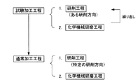
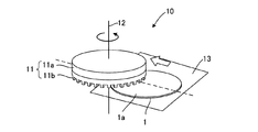
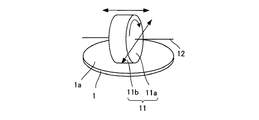
本発明の被研磨物の研磨方法は、半導体ウェハなどの被研磨物1の表面1aを研磨する化学機械研磨(chemical mechanical polishing:CMP)を含む研磨方法である。図1に示すように、本発明の被研磨物の研磨方法は、試験被研磨物1を用いて、化学機械研磨の研磨速度が速くなる、化学機械研磨の前工程の研削の研削方向を求める試験加工工程と、試験加工工程で求められた研削方向にて被研磨物1の表面1aを研削し、化学機械研磨する通常加工工程と、を含む。なお、研削として、例えば、カップ型の砥石11を用いて、クリープフィード研削を行うことができる(図2A参照)。クリープフィード研削は、大きな切り込み量で、送り速度を小さくし、1パスで目的形状に加工する研削である。あるいは、台金11aの外周面に砥層11bが設けられたストレート型の砥石11を用いて研削を行うこともできる(図2B参照)。研削は、一方向に一回行ってもよいし、一方向に複数回行ってもよい。
The method for polishing an object to be polished according to the present invention is a polishing method including chemical mechanical polishing (CMP) for polishing a
試験加工工程では、一方向に試験被研磨物1と砥石11とを相対移動させることにより、中心軸12を中心に回転する砥石11にて、試験被研磨物1の表面1aを研削する(研削工程:図2A参照)。その後、試験被研磨物1の表面1aを化学機械研磨して、化学機械研磨の研磨速度を求める(化学機械研磨工程:図4参照)。
In the test processing step, the
次に、異なる方向に試験被研磨物1と砥石11とを相対移動させて研削を行い試験被研磨物1の表面1aを化学機械研磨して、化学機械研磨の研磨速度を求める。このように試験被研磨物1と砥石11との相対移動の方向を変えて研削、化学機械研磨を繰り返して、化学機械研磨の研磨速度が速くなる研削方向を求める。
Next, the
なお、試験加工工程において、試験被研磨物1の表面1aがどのような場合に、化学機械研磨の研磨速度が速くなるか分かっている場合には、化学機械研磨をしないで、研削後の試験被研磨物1の表面1aの状態を調べてもよい。表面1aの状態を調べる方法としては、例えば、硬度測定、X線回折等が挙げられる。硬度が小さくなると化学機械研磨の研磨速度が速くなる材料の場合は、硬度が小さくなるような研削方向を求めればよい。
In the test processing step, when it is known what the
通常加工工程では、試験加工工程で求められた研削方向にて、被研磨物1の表面1aを砥石11で研削した後(研削工程:図2A参照)、被研磨物1の表面1aを化学機械研磨する(化学機械研磨工程:図4参照)。試験加工工程は、研削の条件を決める試験的な工程であり、通常加工工程は、製品の製造工程である。
In the normal machining process, after the
本発明の被研磨物の研磨方法では、化学機械研磨の前に被研磨物1の表面1aを一方向に研削するが、その研削方向を適正化することによって、表面1aの状態を改質する。つまり、化学機械研磨の前工程の研削工程において、ある結晶方位に沿って研削することで、被研磨物の表面全体を均一に改質(結晶の転位)できる。改質した表面1aは軟化または脆くなっており、後工程(ラップ、ポリッシュ、CMP)における加工が容易となり、結果として高速加工が実現できる。改質のパラメータは研削方向のみであり、専用の工具や装置が不要である。
In the polishing method for an object to be polished according to the present invention, the
本発明の被研磨物の研磨方法における被研磨物1は、例えば、Si、SiO2等の半導体ウェハや、LN(ニオブ酸リチウム)、LT(タンタル酸リチウム)、GaN等の単結晶ウェハなどである。 The object to be polished 1 in the method for polishing an object to be polished according to the present invention is, for example, a semiconductor wafer such as Si or SiO 2 or a single crystal wafer such as LN (lithium niobate), LT (lithium tantalate), or GaN. is there.
以下、さらに詳しく各工程について説明する。各工程は、試験加工工程においても、通常加工工程においても同様である。被研磨物1と記載しているところは、試験加工工程においては、試験被研磨物1の意味である。なお、試験被研磨物1とは、試験用の試料という意味で、被研磨物1と同じものを用いることができる。
Hereinafter, each process will be described in more detail. Each process is the same in both the test process and the normal process. In the test processing step, what is described as the
(研削工程)
図2Aに、研削装置10の模式図を示す。図2Aに示すように、研削装置10には、砥石11が中心軸12を中心に回転可能に備えられている。図2Aに示す砥石11は、台金11aの下面の外周縁に沿って砥層11bが設けられたカップ型の砥石11である。また、研削装置10は、被研磨物1を固定するためのテーブル13を備える。そして、被研磨物1と砥石11とを相対的に一方向に水平移動させて、被研磨物1を研削する。図2Aでは、砥石11を中心軸12を中心に回転させつつ、被研磨物1の単結晶ウェハをテーブル13にて一方向に水平移動させることにより、単結晶ウェハの表面1aを研削している。図2Aの実施形態では、中心軸12に対して垂直に、被研磨物1を移動させている。
(Grinding process)
FIG. 2A shows a schematic diagram of the grinding
図2Bに他の研削装置10の模式図を示す。図2Bに示す砥石11は、台金11aの外周面に砥層11bが設けられたストレート型の砥石11であり、外周面に設けられた砥層11bによって研削することができる。中心軸12を水平方向とし、中心軸12と被研磨物1とを平行に配置して、被研磨物1または砥石11を移動させて研削する。
FIG. 2B shows a schematic diagram of another grinding
本発明の被研磨物の研磨方法は、研削工程において、砥石11の回転数を500〜5000rpmとすることが好ましい。より好ましくは、2000〜4000rpm、さらに好ましくは、2500〜3500rpmである。砥石11の回転数をこの範囲とすることにより、被研磨物1の表面1aに均一な改質層(変質層)が得られる。被研磨物の研磨方法に用いる砥石11の種類としては、ビトリファイドボンド、メタルボンド、レジンボンド等が挙げられる。
In the method for polishing an object to be polished according to the present invention, the number of revolutions of the
被研磨物1を固定したテーブル13の送り速度は、1〜100mm/minとすることが好ましい。被研磨物1は、テーブル13上に固定されているため、テーブルの送り速度とは、被研磨物1の移動速度である。テーブル13の送り速度は、より好ましくは、10〜80mm/min、さらに好ましくは、20〜60mm/minである。テーブル13の送り速度をこの範囲とすることにより、被研磨物1の表面1aに均一な改質層(変質層)が得られる。
The feed rate of the table 13 to which the
研削工程における切り込み量は、0.1〜50μmとすることが好ましい。より好ましくは、1〜40μm、さらに好ましくは、10〜30μmである。切り込み量をこの範囲とすることにより、被研磨物1の表面1aに均一な改質層(変質層)が得られる。
The cutting amount in the grinding step is preferably 0.1 to 50 μm. More preferably, it is 1-40 micrometers, More preferably, it is 10-30 micrometers. By setting the cut amount within this range, a uniform modified layer (deformed layer) can be obtained on the
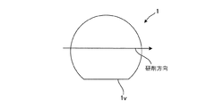
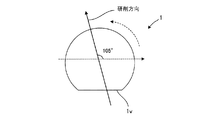
試験加工工程では、被研磨物1の研削方向をある一方向として研削し、それを化学機械研磨して、研磨速度を求める。ここで、研削方向について説明する。研削方向とは、被研磨物1が単結晶ウェハである場合には、オリエンテーションフラット1vに対する方向で定義することにする。図2Cに示すように、オリエンテーションフラット1vに平行に研削した場合を0度とする。図2Dに示すように、反時計方向に研削方向がずれた角度を、研削方向の角度とする。図2Dは、研削方向が105度の場合を示す。
In the test processing step, the grinding direction of the
被研磨物1が、タンタル酸リチウム(LT)のY35〜55度面の単結晶ウェハである場合、化学機械研磨の研磨速度が速くなる研削方向は、単結晶ウェハのオリエンテーションフラット1vに対して、100〜110度、好ましくは、105度の方向である(図2D参照)。この方向にタンタル酸リチウムの単結晶ウェハを研削することにより、化学機械研磨による研磨速度を速くすることができる。
When the
(ラップ工程)
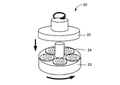
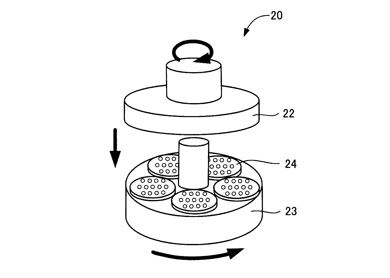
本発明の被研磨物の研磨方法は、図2Aの研削工程の後、化学機械研磨工程を行うが、研削工程の後、化学機械研磨工程の前にラップ工程を行ってもよい。図3にラップ工程を行うためのラップ加工装置を示す。図3に示すように、ラップ加工装置は、上定盤22と、この上定盤22に対向するように配置され、回転する下定盤23と、これらの間に挟み込まれる円盤形状のキャリア24と、を有する。キャリア24の下面に被研磨物1を配置し、上定盤22と下定盤23とで被研磨物1を挟み、砥粒で研磨して平坦性を高める。
(Lapping process)
In the polishing method for an object to be polished according to the present invention, a chemical mechanical polishing step is performed after the grinding step of FIG. 2A, but a lapping step may be performed after the grinding step and before the chemical mechanical polishing step. FIG. 3 shows a lapping apparatus for performing the lapping process. As shown in FIG. 3, the lapping apparatus includes an
(化学機械研磨工程)
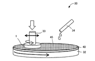
図4に、化学機械研磨に用いるCMP装置30の模式図を示す。CMP装置30は、定盤32、研磨ヘッド33、スラリー供給装置34を備える。定盤32には、研磨パッド40が取り付けられている。スラリー供給装置34からは、スラリーが研磨パッド40上に供給され、定盤32が回転するとともに、研磨ヘッド33が、研磨パッド40上に配置された被研磨物1を研磨パッド40に対して押しつけつつ定盤32と同方向に回転することにより、被研磨物1の表面1aを化学的及び機械的に研磨する。
(Chemical mechanical polishing process)
FIG. 4 shows a schematic diagram of a
本発明の研磨パッド40は、研磨パッド40は、円板状に形成され、その表面には、複数の溝45が加工されており、定盤32に取り付けられて被研磨物1を研磨するものである。研磨パッド40は、例えば、発泡硬質ウレタン、スウェード等で形成されている。溝45の数、深さ、幅等は、被研磨物1の種類、研磨目的などによって適宜選択することができる。しかしながら、例えば、溝45の幅は、0.2〜1.5mm、溝45のピッチ(溝45の中心間の距離)は、1〜20mm程度のものを利用することができる。
The
化学機械研磨工程における研磨パッド40の回転数は、10〜300rpmであることが好ましい。より好ましくは、20〜150rpm、さらに好ましくは、30〜100rpmである。研磨パッド40の回転数をこの範囲とすることにより、被研磨物1の研磨量を面内において均一にできる。
The number of rotations of the
化学機械研磨工程における被研磨物1の回転数は、10〜300rpmとすることが好ましい。より好ましくは、20〜150rpm、さらに好ましくは、30〜100rpmである。被研磨物1の回転数をこの範囲とすることにより、被研磨物1の研磨量を面内において均一にできる。
The number of rotations of the
被研磨物1を研磨パッド40に押しつける荷重は、0.5〜100kPaとすることが好ましい。より好ましくは、5〜50kPa、さらに好ましくは、10〜30kPaである。荷重をこの範囲とすることにより、被研磨物1の研磨量を面内において均一にできる。
The load for pressing the
スラリーは、CMP装置30のスラリー供給装置34から、研磨パッド40の表面上に供給する。スラリーは、研磨材、酸、酸化剤、および水を含む。研磨材としてコロイダルシリカ、ヒュームドシリカ、アルミナ、チタニア、ジルコニアおよびこれらの混合物等を利用することができる。また、酸化剤としては、過酸化物、硝酸塩等を利用することができる。さらに、スラリーには、pH調整剤を含んでもよい。pH調整剤は、スラリーのpHを所望の値に調整するために酸性物質又は塩基性物質を適宜使用する。
The slurry is supplied onto the surface of the
スラリー供給装置34から、スラリーを研磨パッド40上に供給し、定盤32が回転するとともに、研磨ヘッド33が、研磨パッド40上に配置された被研磨物1を研磨パッド40に対して押しつけつつ定盤32と同方向に回転することにより、被研磨物1の表面1aを化学的及び機械的に研磨する。
The slurry is supplied from the
以下、本発明を実施例に基づいてさらに詳細に説明するが、本発明はこれらの実施例に限定されるものではない。 EXAMPLES Hereinafter, although this invention is demonstrated further in detail based on an Example, this invention is not limited to these Examples.
被研磨物1として、Y40度タンタル酸リチウムの単結晶ウェハを用意した。
As the
(実施例1,比較例1)
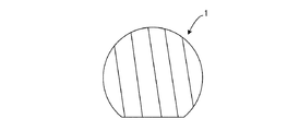
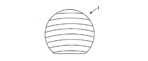
タンタル酸リチウムの単結晶ウェハの表面1aを、一方向に研削した。砥石11は、ダイヤモンド#1000、ビトリファイドボンド砥石を用いた。砥石11の回転数は、2500rpm、被研磨物1を固定したテーブルの送り速度は、20mm/min、切り込み量は、5μmとした。単結晶ウェハのオリエンテーションフラット1vに対する研削方向は、0,105度とした(図2C,2D参照)。図5に、研削方向が105度の場合の被研磨物1(単結晶ウェハ)の表面の加工痕、図6に、研削方向が0度の場合の被研磨物1(単結晶ウェハ)の表面の加工痕を示す。
(Example 1, Comparative Example 1)
The
(硬度)
研削後の単結晶ウェハの表面1aの硬度は、115°三角すい圧子によるマルテンス硬さ(HMT115)にて評価した。
(hardness)
The hardness of the
(化学機械研磨)
研削後の単結晶ウェハの表面1aを化学機械研磨した。化学機械研磨の条件は、次の通りである。研磨パッド40の回転数は、100rpmとした。単結晶ウェハの回転数は、100rpmとした。単結晶ウェハを研磨パッド40に押しつける荷重は、15kPaとした。スラリーは、研磨材としてコロイダルシリカを含むものを用いた。研磨前後の単結晶ウェハの厚みを測定することにより、化学機械研磨の研磨速度を求めた。
(Chemical mechanical polishing)
The
(比較例2)
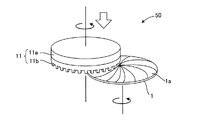
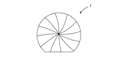
従来の研削装置50により研削した。図7Aに従来の研磨装置50を示す。中心軸12を中心に回転する砥石11にて被研磨物1を回転させながら研削した。実施例1と同様にしてその表面の状態や化学機械研磨の研磨速度を調べた。図7Bに、従来の研削装置による被研磨物の表面の加工痕を示す。
(Comparative Example 2)
Grinding was performed with a conventional
実施例1では、硬度が低くなり、化学機械研磨の研磨速度が、比較例1や比較例2よりも速くなった。研削方法を、一般的なインフィード研削(比較例2)から、クリープフィード研削とすることにより、単結晶ウェハの表面全体を均一に改質することができた。また、クリープフィード研削の研削方向をある特定の一方向とすることにより、後工程の化学機械研磨の研磨速度を速くすることができた。 In Example 1, the hardness was low, and the polishing rate of chemical mechanical polishing was faster than Comparative Example 1 and Comparative Example 2. By changing the grinding method from general in-feed grinding (Comparative Example 2) to creep feed grinding, the entire surface of the single crystal wafer could be uniformly modified. In addition, by setting the grinding direction of creep feed grinding to one specific direction, the polishing rate of chemical mechanical polishing in the subsequent process could be increased.
本発明の被研磨物の研磨方法は、半導体ウェハ等の被研磨物の表面の研磨に用いることができる。 The method for polishing an object to be polished according to the present invention can be used for polishing the surface of an object to be polished such as a semiconductor wafer.
1:(試験)被研磨物、1a:(被研磨物の)表面、1v:オリエンテーションフラット、10:研削装置、11:砥石、11a:台金、11b:砥層、12:中心軸、13:テーブル、20:ラップ加工装置、22:上定盤、23:下定盤、24:キャリア、30:CMP装置、32:定盤、33:研磨ヘッド、34:スラリー供給装置、40:研磨パッド、45:溝、50:研磨装置。 1: (test) object to be polished, 1a: surface (of object to be polished), 1v: orientation flat, 10: grinding device, 11: grinding wheel, 11a: base metal, 11b: abrasive layer, 12: central axis, 13: Table: 20: Lapping device, 22: Upper surface plate, 23: Lower surface plate, 24: Carrier, 30: CMP device, 32: Surface plate, 33: Polishing head, 34: Slurry supply device, 40: Polishing pad, 45 : Groove, 50: polishing apparatus.
Claims (2)
前記試験被研磨物の前記表面を化学機械研磨して前記化学機械研磨の研磨速度を求め、または、前記表面の状態を調べ、
前記試験被研磨物と前記砥石との相対移動の方向を変えて同様のことを繰り返して、前記化学機械研磨の前記研磨速度が速くなる研削方向を求める試験加工工程と、
前記試験加工工程で求められた前記研削方向にて、被研磨物の前記表面を前記砥石で研削した後、前記被研磨物の前記表面を前記化学機械研磨する通常加工工程と、
を含む被研磨物の研磨方法。 By relatively moving the test object and the grindstone in one direction, the surface of the test object is ground with the grindstone rotating around the central axis.
The surface of the test workpiece is chemically mechanically polished to determine the polishing rate of the chemical mechanical polishing, or the state of the surface is examined,
A test processing step for obtaining a grinding direction in which the polishing speed of the chemical mechanical polishing is increased by repeating the same by changing the direction of relative movement between the test workpiece and the grindstone,
In the grinding direction determined in the test processing step, after grinding the surface of the object to be polished with the grindstone, the normal processing step of chemical mechanical polishing the surface of the object to be polished;
A method for polishing an object to be polished.
前記化学機械研磨の研磨速度が速くなる前記研削方向が、前記単結晶ウェハのオリエンテーションフラットに対して、100〜110度の方向であり、
前記研削方向に前記被研磨物と前記砥石とを相対的に水平移動させて前記被研磨物の前記表面を研磨する請求項1に記載の被研磨物の研磨方法。 The object to be polished is a single crystal wafer having a Y35 to 55 degree plane of lithium tantalate,
The grinding direction in which the polishing rate of the chemical mechanical polishing is increased is a direction of 100 to 110 degrees with respect to the orientation flat of the single crystal wafer,
The method for polishing an object according to claim 1, wherein the surface of the object to be polished is polished by relatively horizontally moving the object to be polished and the grindstone in the grinding direction.
Priority Applications (1)
| Application Number | Priority Date | Filing Date | Title |
|---|---|---|---|
| JP2011272534A JP2013123763A (en) | 2011-12-13 | 2011-12-13 | Polishing method for object to be polished |
Applications Claiming Priority (1)
| Application Number | Priority Date | Filing Date | Title |
|---|---|---|---|
| JP2011272534A JP2013123763A (en) | 2011-12-13 | 2011-12-13 | Polishing method for object to be polished |
Publications (1)
| Publication Number | Publication Date |
|---|---|
| JP2013123763A true JP2013123763A (en) | 2013-06-24 |
Family
ID=48775336
Family Applications (1)
| Application Number | Title | Priority Date | Filing Date |
|---|---|---|---|
| JP2011272534A Pending JP2013123763A (en) | 2011-12-13 | 2011-12-13 | Polishing method for object to be polished |
Country Status (1)
| Country | Link |
|---|---|
| JP (1) | JP2013123763A (en) |
Cited By (2)
| Publication number | Priority date | Publication date | Assignee | Title |
|---|---|---|---|---|
| WO2023276036A1 (en) * | 2021-06-30 | 2023-01-05 | 京セラ株式会社 | Method for manufacturing gallium nitride single crystal substrate and method for manufacturing nitride single crystal substrate of group 13 element of periodic table |
| CN116352511A (en) * | 2023-04-10 | 2023-06-30 | 南通军盛机械模具有限公司 | Novel roller sanding process for container side plate |
-
2011
- 2011-12-13 JP JP2011272534A patent/JP2013123763A/en active Pending
Cited By (3)
| Publication number | Priority date | Publication date | Assignee | Title |
|---|---|---|---|---|
| WO2023276036A1 (en) * | 2021-06-30 | 2023-01-05 | 京セラ株式会社 | Method for manufacturing gallium nitride single crystal substrate and method for manufacturing nitride single crystal substrate of group 13 element of periodic table |
| US12290899B2 (en) | 2021-06-30 | 2025-05-06 | Kyocera Corporation | Method of manufacturing gallium nitride single-crystal substrate and method of manufacturing single-crystal substrate of nitride of group 13 element in periodic table |
| CN116352511A (en) * | 2023-04-10 | 2023-06-30 | 南通军盛机械模具有限公司 | Novel roller sanding process for container side plate |
Similar Documents
| Publication | Publication Date | Title |
|---|---|---|
| JP5635957B2 (en) | Polishing method of polishing object and polishing pad | |
| CN111630213B (en) | Seed crystal for growing single crystal 4H-SiC and processing method thereof | |
| KR100818683B1 (en) | Mirror chamfering wafer, mirror chamfering polishing cloth and mirror chamfering polishing device and method | |
| JP7045676B1 (en) | Semiconductor crystal wafer manufacturing equipment and manufacturing method | |
| JP3924641B2 (en) | Manufacturing method of semiconductor wafer | |
| JP2015082539A (en) | Semiconductor wafer manufacturing method | |
| JP2016203342A (en) | Method for manufacturing truer and method for manufacturing semiconductor wafer, and chamfering device for semiconductor wafer | |
| WO2001022484A1 (en) | Method of manufacturing semiconductor wafer | |
| JP2010021394A (en) | Method of manufacturing semiconductor wafer | |
| JP7072180B1 (en) | Manufacturing method and equipment for semiconductor crystal wafers | |
| CN114667594A (en) | Method for polishing wafer and silicon wafer | |
| KR20150073214A (en) | Method for producing polished article | |
| WO2023053476A1 (en) | Method and apparatus for producing semiconductor crystal wafer | |
| JP2002066905A (en) | Semiconductor device manufacturing method and device | |
| JP5944581B2 (en) | Semiconductor wafer grinding apparatus, semiconductor wafer manufacturing method, and semiconductor wafer grinding method | |
| JP7041932B1 (en) | Manufacturing method and equipment for semiconductor crystal wafers | |
| JP7104909B1 (en) | Semiconductor crystal wafer manufacturing method and manufacturing apparatus | |
| JP2010173016A (en) | Conditioner for semiconductor polishing cloth, method for manufacturing the conditioner for semiconductor polishing cloth, and semiconductor polishing apparatus | |
| US6866560B1 (en) | Method for thinning specimen | |
| JP2001007064A (en) | Grinding method of semiconductor wafer | |
| WO2000024548A1 (en) | Polishing apparatus and a semiconductor manufacturing method using the same | |
| JPH07100737A (en) | Method for polishing semiconductor wafer | |
| JP2023094222A (en) | Method for manufacturing semiconductor crystal wafer and manufacturing equipment | |
| JP7007625B1 (en) | Manufacturing method and equipment for semiconductor crystal wafers | |
| KR20170087300A (en) | Edge grinding apparatus |