JP2013200548A - 再帰性反射体成形型および再帰反射微細構造を製作するための方法およびその装置 - Google Patents
再帰性反射体成形型および再帰反射微細構造を製作するための方法およびその装置 Download PDFInfo
- Publication number
- JP2013200548A JP2013200548A JP2012213503A JP2012213503A JP2013200548A JP 2013200548 A JP2013200548 A JP 2013200548A JP 2012213503 A JP2012213503 A JP 2012213503A JP 2012213503 A JP2012213503 A JP 2012213503A JP 2013200548 A JP2013200548 A JP 2013200548A
- Authority
- JP
- Japan
- Prior art keywords
- retroreflective
- microstructured pattern
- retroreflector
- mold
- photosensitive coating
- Prior art date
- Legal status (The legal status is an assumption and is not a legal conclusion. Google has not performed a legal analysis and makes no representation as to the accuracy of the status listed.)
- Pending
Links
- 238000000034 method Methods 0.000 title claims abstract description 115
- 238000000576 coating method Methods 0.000 claims abstract description 62
- 239000011248 coating agent Substances 0.000 claims abstract description 61
- 239000000758 substrate Substances 0.000 claims abstract description 46
- 230000005670 electromagnetic radiation Effects 0.000 claims abstract description 18
- 238000004519 manufacturing process Methods 0.000 claims description 27
- 238000005516 engineering process Methods 0.000 description 25
- 239000000463 material Substances 0.000 description 23
- 230000008569 process Effects 0.000 description 18
- 238000013461 design Methods 0.000 description 14
- 229910003460 diamond Inorganic materials 0.000 description 9
- 239000010432 diamond Substances 0.000 description 9
- 238000003754 machining Methods 0.000 description 9
- 230000003287 optical effect Effects 0.000 description 8
- 229920002120 photoresistant polymer Polymers 0.000 description 7
- 238000005323 electroforming Methods 0.000 description 6
- 229920001296 polysiloxane Polymers 0.000 description 6
- 238000010586 diagram Methods 0.000 description 5
- PXHVJJICTQNCMI-UHFFFAOYSA-N Nickel Chemical compound [Ni] PXHVJJICTQNCMI-UHFFFAOYSA-N 0.000 description 4
- 238000004049 embossing Methods 0.000 description 4
- 229920005989 resin Polymers 0.000 description 4
- 239000011347 resin Substances 0.000 description 4
- 230000015572 biosynthetic process Effects 0.000 description 3
- 238000005266 casting Methods 0.000 description 3
- 238000005520 cutting process Methods 0.000 description 3
- 238000005530 etching Methods 0.000 description 3
- 239000010408 film Substances 0.000 description 3
- 230000010076 replication Effects 0.000 description 3
- 238000012546 transfer Methods 0.000 description 3
- BQCADISMDOOEFD-UHFFFAOYSA-N Silver Chemical compound [Ag] BQCADISMDOOEFD-UHFFFAOYSA-N 0.000 description 2
- 229910000831 Steel Inorganic materials 0.000 description 2
- 230000008901 benefit Effects 0.000 description 2
- 238000001723 curing Methods 0.000 description 2
- 238000011161 development Methods 0.000 description 2
- 230000000694 effects Effects 0.000 description 2
- 239000012467 final product Substances 0.000 description 2
- 238000001746 injection moulding Methods 0.000 description 2
- 238000010884 ion-beam technique Methods 0.000 description 2
- 230000007246 mechanism Effects 0.000 description 2
- 229910052751 metal Inorganic materials 0.000 description 2
- 239000002184 metal Substances 0.000 description 2
- 238000012986 modification Methods 0.000 description 2
- 230000004048 modification Effects 0.000 description 2
- 229910052759 nickel Inorganic materials 0.000 description 2
- 238000012545 processing Methods 0.000 description 2
- 229910052709 silver Inorganic materials 0.000 description 2
- 239000004332 silver Substances 0.000 description 2
- 239000000243 solution Substances 0.000 description 2
- 239000007921 spray Substances 0.000 description 2
- 239000003381 stabilizer Substances 0.000 description 2
- 239000010959 steel Substances 0.000 description 2
- 239000004593 Epoxy Substances 0.000 description 1
- 229920002396 Polyurea Polymers 0.000 description 1
- 229920006397 acrylic thermoplastic Polymers 0.000 description 1
- 229910052782 aluminium Inorganic materials 0.000 description 1
- XAGFODPZIPBFFR-UHFFFAOYSA-N aluminium Chemical compound [Al] XAGFODPZIPBFFR-UHFFFAOYSA-N 0.000 description 1
- 238000003491 array Methods 0.000 description 1
- 238000010420 art technique Methods 0.000 description 1
- 230000005540 biological transmission Effects 0.000 description 1
- 230000008859 change Effects 0.000 description 1
- 239000004020 conductor Substances 0.000 description 1
- 238000004132 cross linking Methods 0.000 description 1
- 230000007547 defect Effects 0.000 description 1
- 230000007812 deficiency Effects 0.000 description 1
- 238000003618 dip coating Methods 0.000 description 1
- 238000001312 dry etching Methods 0.000 description 1
- 239000002659 electrodeposit Substances 0.000 description 1
- 238000001227 electron beam curing Methods 0.000 description 1
- 125000003700 epoxy group Chemical group 0.000 description 1
- 230000006870 function Effects 0.000 description 1
- 239000011521 glass Substances 0.000 description 1
- 238000005304 joining Methods 0.000 description 1
- 230000005499 meniscus Effects 0.000 description 1
- 238000000465 moulding Methods 0.000 description 1
- NJPPVKZQTLUDBO-UHFFFAOYSA-N novaluron Chemical compound C1=C(Cl)C(OC(F)(F)C(OC(F)(F)F)F)=CC=C1NC(=O)NC(=O)C1=C(F)C=CC=C1F NJPPVKZQTLUDBO-UHFFFAOYSA-N 0.000 description 1
- 238000001020 plasma etching Methods 0.000 description 1
- 229920003023 plastic Polymers 0.000 description 1
- 239000004033 plastic Substances 0.000 description 1
- 229920003229 poly(methyl methacrylate) Polymers 0.000 description 1
- 229920000515 polycarbonate Polymers 0.000 description 1
- 239000004417 polycarbonate Substances 0.000 description 1
- 229920000647 polyepoxide Polymers 0.000 description 1
- 229920000728 polyester Polymers 0.000 description 1
- 229920000642 polymer Polymers 0.000 description 1
- 229920002635 polyurethane Polymers 0.000 description 1
- 239000004814 polyurethane Substances 0.000 description 1
- 239000000047 product Substances 0.000 description 1
- 230000005855 radiation Effects 0.000 description 1
- 239000007787 solid Substances 0.000 description 1
- 239000002904 solvent Substances 0.000 description 1
- 238000004528 spin coating Methods 0.000 description 1
- 238000009718 spray deposition Methods 0.000 description 1
- 238000005507 spraying Methods 0.000 description 1
- 238000000992 sputter etching Methods 0.000 description 1
- ISXSCDLOGDJUNJ-UHFFFAOYSA-N tert-butyl prop-2-enoate Chemical compound CC(C)(C)OC(=O)C=C ISXSCDLOGDJUNJ-UHFFFAOYSA-N 0.000 description 1
- 239000010409 thin film Substances 0.000 description 1
- XLYOFNOQVPJJNP-UHFFFAOYSA-N water Substances O XLYOFNOQVPJJNP-UHFFFAOYSA-N 0.000 description 1
Images


Classifications
-
- G—PHYSICS
- G03—PHOTOGRAPHY; CINEMATOGRAPHY; ANALOGOUS TECHNIQUES USING WAVES OTHER THAN OPTICAL WAVES; ELECTROGRAPHY; HOLOGRAPHY
- G03F—PHOTOMECHANICAL PRODUCTION OF TEXTURED OR PATTERNED SURFACES, e.g. FOR PRINTING, FOR PROCESSING OF SEMICONDUCTOR DEVICES; MATERIALS THEREFOR; ORIGINALS THEREFOR; APPARATUS SPECIALLY ADAPTED THEREFOR
- G03F7/00—Photomechanical, e.g. photolithographic, production of textured or patterned surfaces, e.g. printing surfaces; Materials therefor, e.g. comprising photoresists; Apparatus specially adapted therefor
- G03F7/20—Exposure; Apparatus therefor
- G03F7/2051—Exposure without an original mask, e.g. using a programmed deflection of a point source, by scanning, by drawing with a light beam, using an addressed light or corpuscular source
- G03F7/2059—Exposure without an original mask, e.g. using a programmed deflection of a point source, by scanning, by drawing with a light beam, using an addressed light or corpuscular source using a scanning corpuscular radiation beam, e.g. an electron beam
-
- B—PERFORMING OPERATIONS; TRANSPORTING
- B29—WORKING OF PLASTICS; WORKING OF SUBSTANCES IN A PLASTIC STATE IN GENERAL
- B29D—PRODUCING PARTICULAR ARTICLES FROM PLASTICS OR FROM SUBSTANCES IN A PLASTIC STATE
- B29D11/00—Producing optical elements, e.g. lenses or prisms
- B29D11/00605—Production of reflex reflectors
-
- G—PHYSICS
- G02—OPTICS
- G02B—OPTICAL ELEMENTS, SYSTEMS OR APPARATUS
- G02B5/00—Optical elements other than lenses
- G02B5/12—Reflex reflectors
- G02B5/122—Reflex reflectors cube corner, trihedral or triple reflector type
- G02B5/124—Reflex reflectors cube corner, trihedral or triple reflector type plural reflecting elements forming part of a unitary plate or sheet
-
- G—PHYSICS
- G03—PHOTOGRAPHY; CINEMATOGRAPHY; ANALOGOUS TECHNIQUES USING WAVES OTHER THAN OPTICAL WAVES; ELECTROGRAPHY; HOLOGRAPHY
- G03F—PHOTOMECHANICAL PRODUCTION OF TEXTURED OR PATTERNED SURFACES, e.g. FOR PRINTING, FOR PROCESSING OF SEMICONDUCTOR DEVICES; MATERIALS THEREFOR; ORIGINALS THEREFOR; APPARATUS SPECIALLY ADAPTED THEREFOR
- G03F7/00—Photomechanical, e.g. photolithographic, production of textured or patterned surfaces, e.g. printing surfaces; Materials therefor, e.g. comprising photoresists; Apparatus specially adapted therefor
- G03F7/0005—Production of optical devices or components in so far as characterised by the lithographic processes or materials used therefor
-
- G—PHYSICS
- G03—PHOTOGRAPHY; CINEMATOGRAPHY; ANALOGOUS TECHNIQUES USING WAVES OTHER THAN OPTICAL WAVES; ELECTROGRAPHY; HOLOGRAPHY
- G03F—PHOTOMECHANICAL PRODUCTION OF TEXTURED OR PATTERNED SURFACES, e.g. FOR PRINTING, FOR PROCESSING OF SEMICONDUCTOR DEVICES; MATERIALS THEREFOR; ORIGINALS THEREFOR; APPARATUS SPECIALLY ADAPTED THEREFOR
- G03F7/00—Photomechanical, e.g. photolithographic, production of textured or patterned surfaces, e.g. printing surfaces; Materials therefor, e.g. comprising photoresists; Apparatus specially adapted therefor
- G03F7/20—Exposure; Apparatus therefor
- G03F7/24—Curved surfaces
-
- G—PHYSICS
- G03—PHOTOGRAPHY; CINEMATOGRAPHY; ANALOGOUS TECHNIQUES USING WAVES OTHER THAN OPTICAL WAVES; ELECTROGRAPHY; HOLOGRAPHY
- G03F—PHOTOMECHANICAL PRODUCTION OF TEXTURED OR PATTERNED SURFACES, e.g. FOR PRINTING, FOR PROCESSING OF SEMICONDUCTOR DEVICES; MATERIALS THEREFOR; ORIGINALS THEREFOR; APPARATUS SPECIALLY ADAPTED THEREFOR
- G03F7/00—Photomechanical, e.g. photolithographic, production of textured or patterned surfaces, e.g. printing surfaces; Materials therefor, e.g. comprising photoresists; Apparatus specially adapted therefor
- G03F7/26—Processing photosensitive materials; Apparatus therefor
- G03F7/30—Imagewise removal using liquid means
Landscapes
- Physics & Mathematics (AREA)
- General Physics & Mathematics (AREA)
- Engineering & Computer Science (AREA)
- Health & Medical Sciences (AREA)
- Ophthalmology & Optometry (AREA)
- Mechanical Engineering (AREA)
- Manufacturing & Machinery (AREA)
- Toxicology (AREA)
- Optics & Photonics (AREA)
- Optical Elements Other Than Lenses (AREA)
- Moulds For Moulding Plastics Or The Like (AREA)
- Application Of Or Painting With Fluid Materials (AREA)
- Shaping Of Tube Ends By Bending Or Straightening (AREA)
Abstract
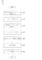
【解決手段】段階12で、表面上に感光性コーティングを有する基板が提供される。段階14で、表面レリーフ微細構造化パターンは、感光性コーティングを電磁放射線のビームに選択的に露光することによって感光性コーティングにおいて作り出される。段階16で、感光性コーティングの露光部分は現像されて、段階18で、基板の表面に再帰反射微細構造化パターンを形成する。段階20、22で、再帰反射微細構造化パターンは、その表面に再帰反射微細構造化パターンを備える再帰性反射体成形型に転写される。次いで段階24で、連続的な再帰反射微細構造化パターンに形成された複数の再帰性反射体を有する継ぎ目のない再帰反射シートが、再帰性反射体成形型から形成される。
【選択図】図1
Description
本発明(1)は、
その少なくとも1つの表面に感光性コーティングを有する基板を提供する工程と、
前記感光性コーティングを電磁放射線のビームに選択的に露光することによって前記感光性コーティングに表面レリーフ微細構造化パターンを作り出す工程と、
前記感光性コーティングの前記露光された部分を現像して、前記基板の表面に再帰反射微細構造化パターンを形成する工程と、
その表面に前記再帰反射微細構造化パターンを備える再帰性反射体成形型に前記再帰反射微細構造化パターンを転写する工程と
を含む、再帰性反射体成形型を製作するための方法である。
本発明(2)は、前記表面レリーフ微細構造化パターンを作り出す工程が、レーザによるパターン生成を含む、本発明(1)の方法である。
本発明(3)は、前記レーザによるパターン生成が、ロードされたビットマップファイルに基づいてコンピュータシステムによって制御される、本発明(2)の方法である。
本発明(4)は、前記再帰反射微細構造化パターンが、三角形、六角形、五角形、または矩形の突出開口再帰性反射体を備える、本発明(1)の方法である。
本発明(5)は、前記再帰反射微細構造化パターンが、複数の種類の再帰性反射体を備える、本発明(1)の方法である。
本発明(6)は、前記再帰反射微細構造化パターンが、傾き、回転、高さ、およびサイズにおいて変化を有する個々のプリズムを備える、本発明(5)の方法である。
本発明(7)は、前記再帰反射微細構造化パターンが、プリズム、レンズ、レンチキュラー、スタンドオフ、構造用部材、平らな領域、またはアールを備える、本発明(1)の方法である。
本発明(8)は、前記基板が、円筒形ドラムを含む、本発明(1)の方法である。
本発明(9)は、前記表面レリーフ微細構造化パターンを作り出す工程が、電磁放射線のビームが前記円筒形ドラムの回転軸に沿って前記感光性コーティングを選択的に露光する際に、前記円筒形ドラムを回転させることを含む、本発明(8)の方法である。
本発明(10)は、前記再帰反射微細構造化パターンを転写する工程が、円筒形の再帰性反射体成形型を形成する、本発明(1)の方法である。
本発明(11)は、
その表面に感光性コーティングを有する基板を提供する工程と、
前記感光性コーティングを電磁放射線のビームに選択的に露光することによって前記感光性コーティングに表面レリーフ微細構造化パターンを作り出す工程と、
前記感光性コーティングの前記露光された部分を現像して、前記基板の表面に再帰反射微細構造化パターンを形成する工程と、
その表面に前記再帰反射微細構造化パターンを備える再帰性反射体成形型に前記再帰反射微細構造化パターンを転写する工程と、
前記再帰性反射体成形型から、表面に前記再帰反射微細構造化パターンを含む再帰反射シートを形成する工程と
を含む、再帰反射シートを製作するための方法である。
本発明(12)は、前記表面レリーフ再帰反射微細構造化パターンを作り出す工程が、レーザによるパターン生成を含む、本発明(11)記載の方法である。
本発明(13)は、前記レーザによるパターン生成が、ロードされたビットマップファイルを有するコンピュータシステムによって制御される、本発明(12)の方法である。
本発明(14)は、前記再帰反射微細構造化パターンが、三角形、六角形、五角形、または矩形の突出開口再帰性反射体を備える、本発明(11)の方法である。
本発明(15)は、前記再帰反射微細構造化パターンが、複数の種類の再帰性反射体を備える、本発明(11)の方法である。
本発明(16)は、前記再帰反射微細構造化パターンが、傾き、回転、高さ、およびサイズにおいて変化を有する個々のプリズムを備える、本発明(15)の方法である。
本発明(17)は、前記再帰反射微細構造化パターンが、プリズム、レンズ、レンチキュラー、スタンドオフ、構造用部材、平らな領域、またはアールを備える、本発明(11)の方法である。
本発明(18)は、前記基板が、円筒形ドラムを含む、本発明(11)の方法である。
本発明(19)は、前記表面レリーフ微細構造化パターンを作り出す工程が、電磁放射線のビームが前記円筒形ドラムの回転軸に沿って前記感光性コーティングを選択的に露光する際に、前記円筒形ドラムを回転させることを含む、本発明(18)の方法である。
本発明(20)は、前記再帰反射微細構造化パターンを転写する工程が、円筒形の再帰性反射体成形型を形成する、本発明(11)の方法である。
本発明(21)は、前記再帰反射シートが、その表面上に前記再帰反射微細構造化パターンのある継ぎ目のないシートを含む、本発明(11)の方法である。
本発明(22)は、複数の再帰性反射体が連続的な再帰反射微細構造化パターンで形成されている、光を再帰反射するように構成された表面を有する複数の再帰性反射体を備える継ぎ目のない再帰反射シートである。
本発明(23)は、前記再帰反射微細構造化パターンが、三角形、六角形、五角形、または矩形の突出開口再帰性反射体を備える、本発明(22)の再帰反射シートである。
本発明(24)は、前記再帰反射微細構造化パターンが、複数の種類の再帰性反射体を備える、本発明(22)の再帰反射シートである。
本発明(25)は、前記再帰反射微細構造化パターンが、傾き、回転、高さ、およびサイズにおいて変化を有する個々のプリズムを備える、本発明(24)の再帰反射シートである。
本発明(26)は、前記再帰反射微細構造化パターンが、プリズム、レンズ、レンチキュラー、スタンドオフ、構造用部材、平らな領域、またはアールを備える、本発明(22)の再帰反射シートである。
本発明(27)は、前記複数の再帰性反射体が、非垂直壁を備える、本発明(22)の再帰反射シートである。
本発明(28)は、前記再帰反射微細構造化パターンが、個々の再帰性反射体を接続する1つまたは複数の流路を備える、本発明(22)の再帰反射シートである。
本技術は、再帰反射微細構造化パターンを含む再帰性反射体成形型および再帰反射シートを製作するための方法を提供する。
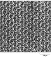
図5のフォーマットのプリズムアレイレイアウトを含んだ再帰性反射体が設計された。ビットマップファイルは、設計の高さに対応するように作成された。つまり、白は設計の一番上の位置にあり、黒は設計の最も深い、つまり一番下の位置にある。設計は、ドラムレーザライタ(DLW)上のレーザの出力設定値に等しい1マイクロメートルの解像度で設計のあらゆる要素を作ることによって工作機械フォーマットに変換された。特に、DLWは、YAGレーザを使用して、鋼円筒基板上に提供されたポジ型フォトレジストコーティングに表面レリーフ再帰反射微細構造化パターンを生成するために使用された。ドラムが回転され、かつレーザ出力が変調されて、設計に従ってフォトレジストを露光した。フォトレジストの現像後、図5の再帰反射微細構造化パターンがマスタシリンダ上に得られた。マスタシリンダは、シリコーンで鋳造された。シリコーンモールドは、次いで銀液吹き付けおよび電鋳プロセスを使用して複製され、図5の微細構造化パターンを含む継ぎ目のない再帰性反射体成形型を作り出した。
12:段階
14:段階
16:段階
18:段階
20:段階
22:段階
24:段階
26:円筒形ドラム
30:ドラムレーザライタ(DLW)
32:円筒形ドラム
34:回転軸
36:レーザ
38:トラック
40:ドラムレーザライタ(DLW)
42:円筒形基板
44:挿入図
46:再帰性反射体成形型
48:挿入図
50:露光源
52:強度安定装置
54:強度変調器
56:コンピュータ制御システム
58:プロセッサ
60:変調器ドライバ
62:台コントローラ
64:移動載物台
66:調時機構
68:ビームエキスパンダ
70:集束対物レンズ
72:検出器
74:オートフォーカスソース
Claims (28)
- その少なくとも1つの表面に感光性コーティングを有する基板を提供する工程と、
前記感光性コーティングを電磁放射線のビームに選択的に露光することによって前記感光性コーティングに表面レリーフ微細構造化パターンを作り出す工程と、
前記感光性コーティングの前記露光された部分を現像して、前記基板の表面に再帰反射微細構造化パターンを形成する工程と、
その表面に前記再帰反射微細構造化パターンを備える再帰性反射体成形型に前記再帰反射微細構造化パターンを転写する工程と
を含む、再帰性反射体成形型を製作するための方法。 - 前記表面レリーフ微細構造化パターンを作り出す工程が、レーザによるパターン生成を含む、請求項1に記載の方法。
- 前記レーザによるパターン生成が、ロードされたビットマップファイルに基づいてコンピュータシステムによって制御される、請求項2に記載の方法。
- 前記再帰反射微細構造化パターンが、三角形、六角形、五角形、または矩形の突出開口再帰性反射体を備える、請求項1に記載の方法。
- 前記再帰反射微細構造化パターンが、複数の種類の再帰性反射体を備える、請求項1に記載の方法。
- 前記再帰反射微細構造化パターンが、傾き、回転、高さ、およびサイズにおいて変化を有する個々のプリズムを備える、請求項5に記載の方法。
- 前記再帰反射微細構造化パターンが、プリズム、レンズ、レンチキュラー、スタンドオフ、構造用部材、平らな領域、またはアールを備える、請求項1に記載の方法。
- 前記基板が、円筒形ドラムを含む、請求項1に記載の方法。
- 前記表面レリーフ微細構造化パターンを作り出す工程が、電磁放射線のビームが前記円筒形ドラムの回転軸に沿って前記感光性コーティングを選択的に露光する際に、前記円筒形ドラムを回転させることを含む、請求項8に記載の方法。
- 前記再帰反射微細構造化パターンを転写する工程が、円筒形の再帰性反射体成形型を形成する、請求項1に記載の方法。
- その表面に感光性コーティングを有する基板を提供する工程と、
前記感光性コーティングを電磁放射線のビームに選択的に露光することによって前記感光性コーティングに表面レリーフ微細構造化パターンを作り出す工程と、
前記感光性コーティングの前記露光された部分を現像して、前記基板の表面に再帰反射微細構造化パターンを形成する工程と、
その表面に前記再帰反射微細構造化パターンを備える再帰性反射体成形型に前記再帰反射微細構造化パターンを転写する工程と、
前記再帰性反射体成形型から、表面に前記再帰反射微細構造化パターンを含む再帰反射シートを形成する工程と
を含む、再帰反射シートを製作するための方法。 - 前記表面レリーフ再帰反射微細構造化パターンを作り出す工程が、レーザによるパターン生成を含む、請求項11記載の方法。
- 前記レーザによるパターン生成が、ロードされたビットマップファイルを有するコンピュータシステムによって制御される、請求項12に記載の方法。
- 前記再帰反射微細構造化パターンが、三角形、六角形、五角形、または矩形の突出開口再帰性反射体を備える、請求項11に記載の方法。
- 前記再帰反射微細構造化パターンが、複数の種類の再帰性反射体を備える、請求項11に記載の方法。
- 前記再帰反射微細構造化パターンが、傾き、回転、高さ、およびサイズにおいて変化を有する個々のプリズムを備える、請求項15に記載の方法。
- 前記再帰反射微細構造化パターンが、プリズム、レンズ、レンチキュラー、スタンドオフ、構造用部材、平らな領域、またはアールを備える、請求項11に記載の方法。
- 前記基板が、円筒形ドラムを含む、請求項11に記載の方法。
- 前記表面レリーフ微細構造化パターンを作り出す工程が、電磁放射線のビームが前記円筒形ドラムの回転軸に沿って前記感光性コーティングを選択的に露光する際に、前記円筒形ドラムを回転させることを含む、請求項18に記載の方法。
- 前記再帰反射微細構造化パターンを転写する工程が、円筒形の再帰性反射体成形型を形成する、請求項11に記載の方法。
- 前記再帰反射シートが、その表面上に前記再帰反射微細構造化パターンのある継ぎ目のないシートを含む、請求項11に記載の方法。
- 複数の再帰性反射体が連続的な再帰反射微細構造化パターンで形成されている、光を再帰反射するように構成された表面を有する複数の再帰性反射体を備える継ぎ目のない再帰反射シート。
- 前記再帰反射微細構造化パターンが、三角形、六角形、五角形、または矩形の突出開口再帰性反射体を備える、請求項22に記載の再帰反射シート。
- 前記再帰反射微細構造化パターンが、複数の種類の再帰性反射体を備える、請求項22に記載の再帰反射シート。
- 前記再帰反射微細構造化パターンが、傾き、回転、高さ、およびサイズにおいて変化を有する個々のプリズムを備える、請求項24に記載の再帰反射シート。
- 前記再帰反射微細構造化パターンが、プリズム、レンズ、レンチキュラー、スタンドオフ、構造用部材、平らな領域、またはアールを備える、請求項22に記載の再帰反射シート。
- 前記複数の再帰性反射体が、非垂直壁を備える、請求項22に記載の再帰反射シート。
- 前記再帰反射微細構造化パターンが、個々の再帰性反射体を接続する1つまたは複数の流路を備える、請求項22に記載の再帰反射シート。
Applications Claiming Priority (2)
| Application Number | Priority Date | Filing Date | Title |
|---|---|---|---|
| US13/428,882 US9050762B2 (en) | 2012-03-23 | 2012-03-23 | Methods for fabricating retroreflector tooling and retroreflective microstructures and devices thereof |
| US13/428,882 | 2012-03-23 |
Publications (2)
| Publication Number | Publication Date |
|---|---|
| JP2013200548A true JP2013200548A (ja) | 2013-10-03 |
| JP2013200548A5 JP2013200548A5 (ja) | 2015-11-12 |
Family
ID=47598692
Family Applications (1)
| Application Number | Title | Priority Date | Filing Date |
|---|---|---|---|
| JP2012213503A Pending JP2013200548A (ja) | 2012-03-23 | 2012-09-27 | 再帰性反射体成形型および再帰反射微細構造を製作するための方法およびその装置 |
Country Status (4)
| Country | Link |
|---|---|
| US (2) | US9050762B2 (ja) |
| EP (1) | EP2641730A3 (ja) |
| JP (1) | JP2013200548A (ja) |
| CN (1) | CN103317627A (ja) |
Cited By (1)
| Publication number | Priority date | Publication date | Assignee | Title |
|---|---|---|---|---|
| JP2018513401A (ja) * | 2015-03-09 | 2018-05-24 | オラフォル アメリカズ インコーポレイテッド | 部分的再帰反射体ツール及びシートを形成する方法並びにその装置 |
Families Citing this family (4)
| Publication number | Priority date | Publication date | Assignee | Title |
|---|---|---|---|---|
| WO2018151964A1 (en) * | 2017-02-14 | 2018-08-23 | 3M Innovative Properties Company | Security articles comprising groups of microstructures made by end milling |
| TWI756466B (zh) | 2017-08-29 | 2022-03-01 | 美商艾維利 丹尼森公司 | 用於基於投影機的顯示系統的回射片 |
| US10969600B2 (en) * | 2018-03-08 | 2021-04-06 | Apple Inc. | Electronic devices with optical markers |
| WO2020242385A1 (en) * | 2019-05-31 | 2020-12-03 | Ams Sensors Singapore Pte. Ltd. | Method of manufacturing a master for a replication process |
Citations (5)
| Publication number | Priority date | Publication date | Assignee | Title |
|---|---|---|---|---|
| JPH1039124A (ja) * | 1996-07-22 | 1998-02-13 | Dainippon Printing Co Ltd | 再帰反射体及びその製造方法 |
| JP2004106320A (ja) * | 2002-09-18 | 2004-04-08 | Ricoh Opt Ind Co Ltd | 微細表面構造をもつ物品の製造方法 |
| JP2005035119A (ja) * | 2003-07-18 | 2005-02-10 | Fuji Photo Film Co Ltd | エンボスロールの製法及び該エンボスロールを使用した転写シートの製法 |
| JP2006315347A (ja) * | 2005-05-13 | 2006-11-24 | Toppan Printing Co Ltd | 光学部品用金型の製造方法およびそれに用いる光学部品用金型の製造装置 |
| JP2007309960A (ja) * | 2006-05-16 | 2007-11-29 | Toppan Printing Co Ltd | ディスプレイ及びその製造方法 |
Family Cites Families (31)
| Publication number | Priority date | Publication date | Assignee | Title |
|---|---|---|---|---|
| US4243618A (en) | 1978-10-23 | 1981-01-06 | Avery International Corporation | Method for forming retroreflective sheeting |
| US5156863A (en) | 1982-09-30 | 1992-10-20 | Stimsonite Corporation | Continuous embossing belt |
| US6258443B1 (en) * | 1994-09-28 | 2001-07-10 | Reflexite Corporation | Textured retroreflective prism structures and molds for forming same |
| US6015214A (en) | 1996-05-30 | 2000-01-18 | Stimsonite Corporation | Retroreflective articles having microcubes, and tools and methods for forming microcubes |
| US6021559A (en) * | 1996-11-01 | 2000-02-08 | 3M Innovative Properties Company | Methods of making a cube corner article master mold |
| US6253442B1 (en) | 1997-07-02 | 2001-07-03 | 3M Innovative Properties Company | Retroreflective cube corner sheeting mold and method for making the same |
| US6120636A (en) * | 1998-01-26 | 2000-09-19 | Reflexite Corporation | Apparatus and method for producing retroreflective material having printed patterns thereon |
| US6410213B1 (en) | 1998-06-09 | 2002-06-25 | Corning Incorporated | Method for making optical microstructures having profile heights exceeding fifteen microns |
| US6322652B1 (en) * | 1998-09-04 | 2001-11-27 | 3M Innovative Properties Company | Method of making a patterned surface articles |
| US6967053B1 (en) * | 1999-01-21 | 2005-11-22 | Reflexite Corporation | Durable, open-faced retroreflective prismatic construction |
| US20050185279A1 (en) * | 1999-01-21 | 2005-08-25 | Reflexite Corporation | Durable, open-faced retroreflective prismatic construction |
| US6576406B1 (en) * | 2000-06-29 | 2003-06-10 | Sarcos Investments Lc | Micro-lithographic method and apparatus using three-dimensional mask |
| US7364314B2 (en) * | 2002-05-15 | 2008-04-29 | Reflexite Corporation | Optical structures |
| US6843571B2 (en) * | 2002-06-11 | 2005-01-18 | 3M Innovative Properties Company | Methods of making a master and replicas thereof |
| US7092160B2 (en) * | 2002-09-12 | 2006-08-15 | Illumina, Inc. | Method of manufacturing of diffraction grating-based optical identification element |
| US7195732B2 (en) | 2002-09-18 | 2007-03-27 | Ricoh Optical Industries Co., Ltd. | Method and mold for fabricating article having fine surface structure |
| US7156527B2 (en) * | 2003-03-06 | 2007-01-02 | 3M Innovative Properties Company | Lamina comprising cube corner elements and retroreflective sheeting |
| US6884371B2 (en) * | 2003-03-06 | 2005-04-26 | 3M Innovative Properties Company | Method of making retroreflective sheeting and articles |
| US7618564B2 (en) * | 2003-03-21 | 2009-11-17 | Ovd Kinegram Ag | Microstructure and method for producing microstructures |
| US7867695B2 (en) * | 2003-09-11 | 2011-01-11 | Bright View Technologies Corporation | Methods for mastering microstructures through a substrate using negative photoresist |
| US20050112472A1 (en) * | 2003-11-20 | 2005-05-26 | Kutsch Wilhelm P. | Seamless holographic embossing substrate produced by laser ablation |
| WO2005114268A2 (en) | 2004-05-12 | 2005-12-01 | Reflexite Corporation | Retroreflective structures |
| US7449280B2 (en) | 2004-05-26 | 2008-11-11 | Microchem Corp. | Photoimageable coating composition and composite article thereof |
| US9272568B2 (en) * | 2005-03-24 | 2016-03-01 | Ryan McDonnell | Method and device for producing registered holographic microstructure refractive and reflective effects |
| US8133644B2 (en) * | 2007-10-31 | 2012-03-13 | 3M Innovative Properties Company | Method of forming an image having multiple phases |
| US8316764B1 (en) * | 2008-05-22 | 2012-11-27 | Teh Ming Eric Wu | Apparatus and method for adding a registered image on a sheeted substrate |
| CN102387915A (zh) * | 2009-02-17 | 2012-03-21 | 伊利诺伊大学评议会 | 柔性微结构超疏水材料 |
| US20120126458A1 (en) * | 2009-05-26 | 2012-05-24 | King William P | Casting microstructures into stiff and durable materials from a flexible and reusable mold |
| WO2011020727A1 (en) * | 2009-08-21 | 2011-02-24 | Basf Se | Apparatus and method for a sub microscopic and optically variable image carrying device |
| JP2012003026A (ja) * | 2010-06-16 | 2012-01-05 | Sony Corp | 光学体、窓材、建具および日射遮蔽装置 |
| US8841119B2 (en) * | 2010-07-22 | 2014-09-23 | Mridangam Research Intellectual Property Trust | Sensor for fast detection of E-coli |
-
2012
- 2012-03-23 US US13/428,882 patent/US9050762B2/en not_active Expired - Fee Related
- 2012-09-27 JP JP2012213503A patent/JP2013200548A/ja active Pending
- 2012-11-22 CN CN2012104802267A patent/CN103317627A/zh active Pending
-
2013
- 2013-01-16 EP EP13151527.2A patent/EP2641730A3/en not_active Withdrawn
-
2015
- 2015-04-30 US US14/701,040 patent/US9910357B2/en not_active Expired - Fee Related
Patent Citations (5)
| Publication number | Priority date | Publication date | Assignee | Title |
|---|---|---|---|---|
| JPH1039124A (ja) * | 1996-07-22 | 1998-02-13 | Dainippon Printing Co Ltd | 再帰反射体及びその製造方法 |
| JP2004106320A (ja) * | 2002-09-18 | 2004-04-08 | Ricoh Opt Ind Co Ltd | 微細表面構造をもつ物品の製造方法 |
| JP2005035119A (ja) * | 2003-07-18 | 2005-02-10 | Fuji Photo Film Co Ltd | エンボスロールの製法及び該エンボスロールを使用した転写シートの製法 |
| JP2006315347A (ja) * | 2005-05-13 | 2006-11-24 | Toppan Printing Co Ltd | 光学部品用金型の製造方法およびそれに用いる光学部品用金型の製造装置 |
| JP2007309960A (ja) * | 2006-05-16 | 2007-11-29 | Toppan Printing Co Ltd | ディスプレイ及びその製造方法 |
Cited By (1)
| Publication number | Priority date | Publication date | Assignee | Title |
|---|---|---|---|---|
| JP2018513401A (ja) * | 2015-03-09 | 2018-05-24 | オラフォル アメリカズ インコーポレイテッド | 部分的再帰反射体ツール及びシートを形成する方法並びにその装置 |
Also Published As
| Publication number | Publication date |
|---|---|
| US9910357B2 (en) | 2018-03-06 |
| US9050762B2 (en) | 2015-06-09 |
| US20130250418A1 (en) | 2013-09-26 |
| US20150234284A1 (en) | 2015-08-20 |
| EP2641730A2 (en) | 2013-09-25 |
| CN103317627A (zh) | 2013-09-25 |
| EP2641730A3 (en) | 2016-09-07 |
Similar Documents
| Publication | Publication Date | Title |
|---|---|---|
| JP5406203B2 (ja) | 浮遊する合成画像を有するシートの形成方法及びマスターツール | |
| JP4401383B2 (ja) | 構造化された素子の製造 | |
| US9910357B2 (en) | Methods for fabricating tooling and sheeting | |
| EP0724740B1 (en) | Retroreflective sheeting material, a method of its production and its use | |
| JP2018513401A (ja) | 部分的再帰反射体ツール及びシートを形成する方法並びにその装置 | |
| CN111065487B (zh) | 制造具有多边形光阑的回射器棱镜的方法及其装置 | |
| WO2001074560A2 (en) | Technique for microstructuring replication moulds | |
| CN104375227A (zh) | 一种多次曝光拼接制作大面积全息光栅的方法 | |
| TW200817834A (en) | Manufacturing a replication tool, sub-master or replica | |
| JP2006171753A (ja) | 微細加工技術を用いたマイクロレンズアレイシート及びその製造方法 | |
| JP4712857B2 (ja) | 傾斜構造体の製造方法、レンズ金型の製造方法およびレンズの製造方法 | |
| JP5595397B2 (ja) | 構造化された対象物の作製および構造化された対象物のための方法および装置 | |
| Fan et al. | 3D printed diffractive optical elements for rapid prototyping | |
| Niesler et al. | 3D Printers for the Fabrication of Micro‐Optical Elements: Disruptive technology enables the way for unprecedented applications | |
| JP2008268451A (ja) | 光学素子、マスター原器、樹脂マスター、樹脂成形品および金型 | |
| JP2013200548A5 (ja) | 成形型および微細構造を製作するための方法およびその装置 | |
| CN218332292U (zh) | 一种激光干涉光刻系统 | |
| JP4296277B2 (ja) | 傾斜構造体の製造方法およびこの方法で製造される金型用母型 | |
| US7092165B2 (en) | Microlens arrays having high focusing efficiency | |
| KR100701355B1 (ko) | 마이크로렌즈 어레이 및 이 마이크로렌즈 어레이의 복제용음각틀의 제작방법 | |
| CN100371738C (zh) | 半色调掩模光刻热熔成形微透镜阵列方法 | |
| Rodríguez et al. | 3D Micro‐Printing Goes Macro: Tailor‐made materials enable pioneering developments and applications | |
| WO2002010805A1 (en) | Microlens arrays having high focusing efficiency | |
| KR20080062154A (ko) | 마이크로 렌즈 제조방법 및 마이크로 렌즈용 마스터제조방법 | |
| Saito et al. | Fabrication process of Morpho-type optical diffuser using feasible double-step design |
Legal Events
| Date | Code | Title | Description |
|---|---|---|---|
| RD04 | Notification of resignation of power of attorney |
Free format text: JAPANESE INTERMEDIATE CODE: A7424 Effective date: 20150515 |
|
| A521 | Request for written amendment filed |
Free format text: JAPANESE INTERMEDIATE CODE: A523 Effective date: 20150925 |
|
| A621 | Written request for application examination |
Free format text: JAPANESE INTERMEDIATE CODE: A621 Effective date: 20150925 |
|
| A977 | Report on retrieval |
Free format text: JAPANESE INTERMEDIATE CODE: A971007 Effective date: 20160629 |
|
| A131 | Notification of reasons for refusal |
Free format text: JAPANESE INTERMEDIATE CODE: A131 Effective date: 20160705 |
|
| A02 | Decision of refusal |
Free format text: JAPANESE INTERMEDIATE CODE: A02 Effective date: 20170216 |