JP2013201210A - 固体撮像装置 - Google Patents
固体撮像装置 Download PDFInfo
- Publication number
- JP2013201210A JP2013201210A JP2012067661A JP2012067661A JP2013201210A JP 2013201210 A JP2013201210 A JP 2013201210A JP 2012067661 A JP2012067661 A JP 2012067661A JP 2012067661 A JP2012067661 A JP 2012067661A JP 2013201210 A JP2013201210 A JP 2013201210A
- Authority
- JP
- Japan
- Prior art keywords
- semiconductor layer
- photoelectric conversion
- imaging device
- state imaging
- solid
- Prior art date
- Legal status (The legal status is an assumption and is not a legal conclusion. Google has not performed a legal analysis and makes no representation as to the accuracy of the status listed.)
- Pending
Links
Images








Classifications
-
- H—ELECTRICITY
- H10—SEMICONDUCTOR DEVICES; ELECTRIC SOLID-STATE DEVICES NOT OTHERWISE PROVIDED FOR
- H10F—INORGANIC SEMICONDUCTOR DEVICES SENSITIVE TO INFRARED RADIATION, LIGHT, ELECTROMAGNETIC RADIATION OF SHORTER WAVELENGTH OR CORPUSCULAR RADIATION
- H10F30/00—Individual radiation-sensitive semiconductor devices in which radiation controls the flow of current through the devices, e.g. photodetectors
- H10F30/20—Individual radiation-sensitive semiconductor devices in which radiation controls the flow of current through the devices, e.g. photodetectors the devices having potential barriers, e.g. phototransistors
- H10F30/21—Individual radiation-sensitive semiconductor devices in which radiation controls the flow of current through the devices, e.g. photodetectors the devices having potential barriers, e.g. phototransistors the devices being sensitive to infrared, visible or ultraviolet radiation
- H10F30/22—Individual radiation-sensitive semiconductor devices in which radiation controls the flow of current through the devices, e.g. photodetectors the devices having potential barriers, e.g. phototransistors the devices being sensitive to infrared, visible or ultraviolet radiation the devices having only one potential barrier, e.g. photodiodes
- H10F30/223—Individual radiation-sensitive semiconductor devices in which radiation controls the flow of current through the devices, e.g. photodetectors the devices having potential barriers, e.g. phototransistors the devices being sensitive to infrared, visible or ultraviolet radiation the devices having only one potential barrier, e.g. photodiodes the potential barrier being a PIN barrier
- H10F30/2235—Individual radiation-sensitive semiconductor devices in which radiation controls the flow of current through the devices, e.g. photodetectors the devices having potential barriers, e.g. phototransistors the devices being sensitive to infrared, visible or ultraviolet radiation the devices having only one potential barrier, e.g. photodiodes the potential barrier being a PIN barrier the devices comprising Group IV amorphous materials
-
- H—ELECTRICITY
- H10—SEMICONDUCTOR DEVICES; ELECTRIC SOLID-STATE DEVICES NOT OTHERWISE PROVIDED FOR
- H10F—INORGANIC SEMICONDUCTOR DEVICES SENSITIVE TO INFRARED RADIATION, LIGHT, ELECTROMAGNETIC RADIATION OF SHORTER WAVELENGTH OR CORPUSCULAR RADIATION
- H10F30/00—Individual radiation-sensitive semiconductor devices in which radiation controls the flow of current through the devices, e.g. photodetectors
- H10F30/20—Individual radiation-sensitive semiconductor devices in which radiation controls the flow of current through the devices, e.g. photodetectors the devices having potential barriers, e.g. phototransistors
- H10F30/21—Individual radiation-sensitive semiconductor devices in which radiation controls the flow of current through the devices, e.g. photodetectors the devices having potential barriers, e.g. phototransistors the devices being sensitive to infrared, visible or ultraviolet radiation
- H10F30/22—Individual radiation-sensitive semiconductor devices in which radiation controls the flow of current through the devices, e.g. photodetectors the devices having potential barriers, e.g. phototransistors the devices being sensitive to infrared, visible or ultraviolet radiation the devices having only one potential barrier, e.g. photodiodes
- H10F30/222—Individual radiation-sensitive semiconductor devices in which radiation controls the flow of current through the devices, e.g. photodetectors the devices having potential barriers, e.g. phototransistors the devices being sensitive to infrared, visible or ultraviolet radiation the devices having only one potential barrier, e.g. photodiodes the potential barrier being a PN heterojunction
-
- H—ELECTRICITY
- H10—SEMICONDUCTOR DEVICES; ELECTRIC SOLID-STATE DEVICES NOT OTHERWISE PROVIDED FOR
- H10F—INORGANIC SEMICONDUCTOR DEVICES SENSITIVE TO INFRARED RADIATION, LIGHT, ELECTROMAGNETIC RADIATION OF SHORTER WAVELENGTH OR CORPUSCULAR RADIATION
- H10F39/00—Integrated devices, or assemblies of multiple devices, comprising at least one element covered by group H10F30/00, e.g. radiation detectors comprising photodiode arrays
- H10F39/10—Integrated devices
- H10F39/12—Image sensors
- H10F39/18—Complementary metal-oxide-semiconductor [CMOS] image sensors; Photodiode array image sensors
-
- H—ELECTRICITY
- H10—SEMICONDUCTOR DEVICES; ELECTRIC SOLID-STATE DEVICES NOT OTHERWISE PROVIDED FOR
- H10F—INORGANIC SEMICONDUCTOR DEVICES SENSITIVE TO INFRARED RADIATION, LIGHT, ELECTROMAGNETIC RADIATION OF SHORTER WAVELENGTH OR CORPUSCULAR RADIATION
- H10F39/00—Integrated devices, or assemblies of multiple devices, comprising at least one element covered by group H10F30/00, e.g. radiation detectors comprising photodiode arrays
- H10F39/80—Constructional details of image sensors
- H10F39/803—Pixels having integrated switching, control, storage or amplification elements
- H10F39/8033—Photosensitive area
Landscapes
- Light Receiving Elements (AREA)
- Solid State Image Pick-Up Elements (AREA)
- Transforming Light Signals Into Electric Signals (AREA)
Abstract
【解決手段】1つの実施形態によれば、光電変換部を有する固体撮像装置が提供される。光電変換部は、第1の半導体層、第2の半導体層、及び第3の半導体層を有する。固体撮像装置では、D2m3/L2m3×ni3 2/N2<D1M2/L1M2×ni2 2/N2かつ、D1m1/L1m1×ni1 2/N1<D1m2/L1m2×ni2 2/N1が成り立つ。
【選択図】図1
Description
実施形態にかかる固体撮像装置SISについて説明する。
Jrev=Jdiff+JGR
=q√(D/τ)×ni 2/Ndope+qniW/τg
=(少数キャリア拡散項)+(トラップ起因生成電流項)・・・数式1
D=μkBT/q=qτ/m*×kBT/q, L=√(Dτ)・・・数式2
が成立することに注意すれば、数式1の第一項の少数キャリアの拡散に関する項は、
Jdiff=q×Dp/Lp×ni 2/ND+q×Dn/Ln×ni 2/NA
=q{√(kBT/m* p)×ni 2/ND
+√(kBT/m* n)×ni 2/NA} ・・・数式3
のように整理される。ここでkBはボルツマン定数、Tは動作温度を意味する。また、下付きの添え字n,pはそれぞれ電子、ホールを意味する。
ni∝exp(−Eg/(2kBT))・・・数式4
つまり、図26(b)に示すフォトダイオードPD900における例えばP型の半導体層902の材料、すなわちSiよりも光吸収効率が高い材料として、SiよりもバンドギャップEgが小さい材料(例えば、Si1−xGex、0<x≦1)を導入すると、P型の半導体層902において、キャリアの有効質量が小さくなることと、真性キャリア濃度niが増加することで、数式3に示される少数キャリアの拡散に応じた暗電流成分Jdiffが大きな値になり、すべてSiで作られたフォトダイオードPD800(図26(a)参照)よりも暗電流が増加する傾向にある。
√(kBT/m* p)×ni 2/NA∝√(μn)ni 2/NA
≒√(μn)/NA×exp(−Eg/(kBT))・・・数式5
である。数式5に、Siのbulk真性電子移動度μnSiには1450cm2/Vsecを、SiGeの真性電子移動度には、Geのbulk真性電子移動度を3900cm2/VsecとしてGe分率に対して移動度の線形関係を仮定したμnSiGe=1450*0.7+3900*0.3=2185cm2/Vsecを代入する。そして、同様に線形関係を仮定して、SiのバンドギャップEgsi=1.12eVに対して、SiGeのバンドギャップEgSiGe=1.12*0.7+0.69*0.3=0.99eVを数式5に代入する。SiとSiGeの移動度比が不純物濃度Ndopeによらないという粗い見積りでは、少数キャリア拡散に関する積の数式3の比は、数式5の比に還元され、
√(μnSiGe)×exp(−EgSiGe/(kBT))/√(μnSi)×exp(−Egsi/(kBT))=180=(2桁)・・・数式6
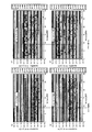
となるので、数式見積り上は、暗電流比は二桁程度増大してしまうと予想される。一方、図27を見ると、SiGeを導入することで3桁程度(1000倍程度)増大してしまうことが認められる。すなわち、SiGeを導入することで、実験的にも理論的にも暗電流は増大することが確認された。
D/L×ni 2/Ndope・・・数式7
の大小関係である。数式7の関係式が、例えば全てSiで作成した場合よりも大きいと、やはり全てSiで作成したよりも暗電流が増加してしまうことに注意したい。
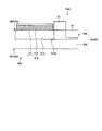
この固体撮像装置SISでは、
D2m3/L2m3×ni3 2/N2<D1M2/L1M2×ni2 2/N2・・・数式8
かつ、
D1m1/L1m1×ni1 2/N1<D1m2/L1m2×ni2 2/N1・・・数式9
が成り立つ。
√(μ2m3)×ni3 2/N2<√(μ1M2)×ni2 2/N2・・・数式10
かつ、
√(μ1m1)×ni1 2/N1<√(μ1m2)×ni2 2/N1・・・数式11
が成り立つ。
Dp3/Lp3×ni3 2/ND<Dp2/Lp2×ni2 2/ND・・・数式12
かつ、
Dn1/Ln1×ni1 2/NA<Dn2/Ln2×ni2 2/NA・・・数式13
が成り立つ。
√(μp3)×ni3 2/ND<√(μp2)×ni2 2/ND・・・数式14
かつ、
√(μn1)×ni1 2/NA<√(μn2)×ni2 2/NA・・・数式15
が成り立つ。
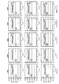
まず、ダングリングボンド等によるキャリアのトラップがない場合(=数式1の少数キャリア拡散項のみに着目する場合)についてシミュレーションを行った。
さて、数式1に記したトラップ起因の電流に関する生成項のうちni/τgの部分(次元1/cm3sec)は、Shockley−Read−Hall(SRH model)によれば、
ni/τg=GRSRH
=(pn−nie 2)/{τgn(p+nieexp(Etrap/kBT))
+τgp(n+nieexp(−Etrap/kBT))}・・・数式16
のように書き下すことができることが知られている。ここで、p、nは、ホール、電子の濃度、τgはトラップに捕獲されたキャリアの寿命で、添え字n、pはそれぞれ電子、ホールのものを意味する。Etrapはトラップの禁制帯内のエネルギー準位で、nieは平衡状態の真性キャリア濃度である。τgは、トラップの濃度Ntrapに反比例することが知られる(1/τg∝Ntrap)。
pn=nie 2・・・数式17
という質量作用則(pn積一定)が成立し、数式16の分子が0になることから容易に理解される。逆に言うと、このpn積一定から著しくずれるところ(=バンドが曲がっているところ)にトラップが大量にあると(トラップ寿命が短いと)、トラップ起因の生成電流が増えるということを意味する。そして、バンドが曲がっている所とは、PD動作時に、バイアスと空間電荷の関数によって空乏層が広がっている領域に他ならない。
L1>√{(kBT/q)μ1m1τ1m1}・・・数式18
を満たすことが好ましい。数式18では、第1の半導体層1のバルク物性の少数キャリアの移動度をμ1m1とし、固体撮像装置SISの動作温度(例えば、最大動作補償運度)をTとし、第1の半導体層1のバルク物性の少数キャリアの運動量緩和時間をτ1m1としている。これは、電流経路長L1が少数キャリア拡散長に比して十分に長いと、アノード電極から弾道的に射出される少数キャリア電流(この場合電子電流)に起因する暗電流が十分無視できるようになるからである。言い換えると、第1の半導体層1の厚さをTH1とした場合、第1の半導体層1の厚さTH1は
TH1>√{(kBT/q)μ1m1τ1m1}・・・数式19
を満たすことが好ましい。L1の具体的な長さのオーダは、図17にLの表として示す。
L3>√{(kBT/q)μ3m3τ3m3}・・・数式20
を満たすことが好ましい。数式20では、第3の半導体層3のバルク物性の少数キャリアの移動度をμ3m3とし、固体撮像装置SISの動作温度(例えば、最大動作補償運度)をTとし、第3の半導体層3のバルク物性の少数キャリアの運動量緩和時間をτ3m3としている。やはり、電流経路長L3が少数キャリア拡散長に比して十分に長いと、カソード電極から弾道的に射出される少数キャリア電流(この場合ホール電流)に起因する暗電流が十分無視できるようになるからである。言い換えると、第3の半導体層3の厚さをTH3とした場合、第3の半導体層3の厚さTH3は
TH3>√{(kBT/q)μ3m3τ3m3}・・・数式21
を満たすことが好ましい。
Dn3/Ln3×ni3 2/NA<Dn2/Ln2×ni2 2/NA・・・数式22
かつ、
Dp1/Lp1×ni1 2/ND<Dp2/Lp2×ni2 2/ND・・・数式23
が成り立つ。
あるいは、上記のように置き換えると、数式10、11は、下記の数式24、25のようになる。固体撮像装置SISでは、
√(μn3)×ni3 2/NA<√(μn2)×ni2 2/NA・・・数式24
かつ、
√(μp1)×ni1 2/ND<√(μp2)×ni2 2/ND・・・数式25
が成り立つ。
次に、実施形態における光電変換部PDの実装形態について図19〜図23を用いて説明する。図19〜図23は、それぞれ、実施形態における光電変換部を適用した固体撮像装置の構成を示す図である。
光電変換部110は、導かれた光に対してPN接合領域で光電変換を行い、光の応じた電荷を発生させて例えば半導体領域113に蓄積する。
Claims (7)
- 光電変換部を備え、
前記光電変換部は、
第1の導電型の第1の半導体層と、
前記第1の半導体層に隣接して配された前記第1の導電型の第2の半導体層と、
前記第2の半導体層に隣接して配された、前記第1の導電型と反対導電型である第2の導電型の第3の半導体層と、
を有し、
前記第2の半導体層の材料の可視光に対する吸収係数は、前記第3の半導体層の材料の可視光に対する吸収係数より高く、
前記第1の半導体層の少数キャリアの拡散係数をD1m1とし、前記第1の半導体層の少数キャリアの拡散長をL1m1とし、前記第1の半導体層の真性キャリア濃度をni1とし、前記第1の半導体層の不純物濃度をN1とし、前記第2の半導体層の少数キャリアの拡散係数をD1m2とし、前記第2の半導体層の多数キャリアの拡散係数をD1M2とし、前記第2の半導体層の少数キャリアの拡散長をL1m2とし、前記第2の半導体層の多数キャリアの拡散長をL1M2とし、前記第2の半導体層の真性キャリア濃度をni2とし、前記第3の半導体層の少数キャリアの拡散係数をD2m3とし、前記第3の半導体層の少数キャリアの拡散長をL2m3とし、前記第3の半導体層の真性キャリア濃度をni3とし、前記第3の半導体層の不純物濃度をN2とするとき、
D2m3/L2m3×ni3 2/N2<D1M2/L1M2×ni2 2/N2
かつ、
D1m1/L1m1×ni1 2/N1<D1m2/L1m2×ni2 2/N1
が成り立つ
ことを特徴とする固体撮像装置。 - 前記光電変換部は、前記第2の半導体層が前記第3の半導体層内に埋め込まれている場合、前記第1の導電型がN型であり前記第2の導電型がP型であり、前記第2の半導体層が前記第3の半導体層の上に設けられている場合、前記第1の導電型がP型であり前記第2の導電型がN型である
ことを特徴とする請求項1に記載の固体撮像装置。 - 前記第2の半導体層の材料のバンドギャップは、前記第1の半導体層の材料のバンドギャップより小さく、かつ、前記第3の半導体層の材料のバンドギャップより小さい
ことを特徴とする請求項1又は2に記載の固体撮像装置。 - 前記第1の半導体層の材料のバンドギャップと前記第3の半導体層の材料のバンドギャップとは、均等である
ことを特徴とする請求項3に記載の固体撮像装置。 - 前記第1の半導体層は、
前記第2の半導体層に隣接する第1の領域と、
前記第1の領域の反対側で前記第2の半導体層に隣接する第2の領域と、
を有し、
前記第3の半導体層は、前記第2の半導体層における前記第1の領域と前記第2の領域との間の部分で前記第2の半導体層に隣接している
ことを特徴とする請求項1から4のいずれか1項に記載の固体撮像装置。 - 前記第2の半導体層は、第1の主面と、前記第1の主面の反対側の第2の主面とを有し、
前記第1の半導体層は、前記第1の主面に配され、
前記第3の半導体層は、前記第2の主面に配され、
前記第1の導電型の不純物の不純物プロファイルは、前記光電変換部において、前記第1の半導体層に近づくことに応じて増加し、前記第1の半導体層内で平坦になっている
ことを特徴とする請求項1から4のいずれか1項に記載の固体撮像装置。 - 前記第1の半導体層の厚さをTH1とし、ボルツマン定数をkBとし、電荷素量をqとし、前記固体撮像装置の動作温度をTとし、前記第1の半導体層における少数キャリアの移動度をμ1m1とし、前記第1の半導体層における少数キャリアの運動量緩和時間をτ1m1とすると、
TH1>√{(kBT/q)μ1m1τ1m1}
を満たす
ことを特徴とする請求項1から6のいずれか1項に記載の固体撮像装置。
Priority Applications (2)
| Application Number | Priority Date | Filing Date | Title |
|---|---|---|---|
| JP2012067661A JP2013201210A (ja) | 2012-03-23 | 2012-03-23 | 固体撮像装置 |
| US13/729,140 US8791542B2 (en) | 2012-03-23 | 2012-12-28 | Solid-state imaging device |
Applications Claiming Priority (1)
| Application Number | Priority Date | Filing Date | Title |
|---|---|---|---|
| JP2012067661A JP2013201210A (ja) | 2012-03-23 | 2012-03-23 | 固体撮像装置 |
Publications (1)
| Publication Number | Publication Date |
|---|---|
| JP2013201210A true JP2013201210A (ja) | 2013-10-03 |
Family
ID=49210930
Family Applications (1)
| Application Number | Title | Priority Date | Filing Date |
|---|---|---|---|
| JP2012067661A Pending JP2013201210A (ja) | 2012-03-23 | 2012-03-23 | 固体撮像装置 |
Country Status (2)
| Country | Link |
|---|---|
| US (1) | US8791542B2 (ja) |
| JP (1) | JP2013201210A (ja) |
Families Citing this family (20)
| Publication number | Priority date | Publication date | Assignee | Title |
|---|---|---|---|---|
| JP2013201210A (ja) * | 2012-03-23 | 2013-10-03 | Toshiba Corp | 固体撮像装置 |
| US9153717B2 (en) * | 2013-08-09 | 2015-10-06 | Taiwan Semiconductor Manufacturing Company, Ltd. | Backside illuminated photo-sensitive device with gradated buffer layer |
| JP2015220339A (ja) * | 2014-05-16 | 2015-12-07 | 株式会社東芝 | 固体撮像装置 |
| US9786715B2 (en) | 2015-07-23 | 2017-10-10 | Artilux Corporation | High efficiency wide spectrum sensor |
| US10707260B2 (en) | 2015-08-04 | 2020-07-07 | Artilux, Inc. | Circuit for operating a multi-gate VIS/IR photodiode |
| TWI723890B (zh) | 2015-08-04 | 2021-04-01 | 光澄科技股份有限公司 | 製造影像感測陣列之方法 |
| US10761599B2 (en) | 2015-08-04 | 2020-09-01 | Artilux, Inc. | Eye gesture tracking |
| US10861888B2 (en) | 2015-08-04 | 2020-12-08 | Artilux, Inc. | Silicon germanium imager with photodiode in trench |
| EP3341970B1 (en) | 2015-08-27 | 2020-10-07 | Artilux Inc. | Wide spectrum optical sensor |
| US10254389B2 (en) | 2015-11-06 | 2019-04-09 | Artilux Corporation | High-speed light sensing apparatus |
| US10741598B2 (en) | 2015-11-06 | 2020-08-11 | Atrilux, Inc. | High-speed light sensing apparatus II |
| US10418407B2 (en) | 2015-11-06 | 2019-09-17 | Artilux, Inc. | High-speed light sensing apparatus III |
| US10886309B2 (en) | 2015-11-06 | 2021-01-05 | Artilux, Inc. | High-speed light sensing apparatus II |
| US10739443B2 (en) | 2015-11-06 | 2020-08-11 | Artilux, Inc. | High-speed light sensing apparatus II |
| US9954133B1 (en) * | 2016-01-15 | 2018-04-24 | Hrl Laboratories, Llc | P-type chalcogenide and N-type silicon heterojunction infrared photodiodes and method of manufacturing thereof |
| TWI788246B (zh) | 2018-02-23 | 2022-12-21 | 美商光程研創股份有限公司 | 光偵測裝置 |
| US11105928B2 (en) | 2018-02-23 | 2021-08-31 | Artilux, Inc. | Light-sensing apparatus and light-sensing method thereof |
| US10886311B2 (en) | 2018-04-08 | 2021-01-05 | Artilux, Inc. | Photo-detecting apparatus |
| US10854770B2 (en) | 2018-05-07 | 2020-12-01 | Artilux, Inc. | Avalanche photo-transistor |
| US10969877B2 (en) | 2018-05-08 | 2021-04-06 | Artilux, Inc. | Display apparatus |
Citations (1)
| Publication number | Priority date | Publication date | Assignee | Title |
|---|---|---|---|---|
| JP2003163361A (ja) * | 2001-11-29 | 2003-06-06 | Mitsubishi Electric Corp | 受光素子および光通信デバイス |
Family Cites Families (3)
| Publication number | Priority date | Publication date | Assignee | Title |
|---|---|---|---|---|
| CA2307745A1 (en) * | 1999-07-15 | 2001-01-15 | Sumitomo Electric Industries, Ltd. | Photodiode |
| JP4639212B2 (ja) | 2006-09-20 | 2011-02-23 | 富士フイルム株式会社 | 裏面照射型撮像素子の製造方法 |
| JP2013201210A (ja) * | 2012-03-23 | 2013-10-03 | Toshiba Corp | 固体撮像装置 |
-
2012
- 2012-03-23 JP JP2012067661A patent/JP2013201210A/ja active Pending
- 2012-12-28 US US13/729,140 patent/US8791542B2/en not_active Expired - Fee Related
Patent Citations (1)
| Publication number | Priority date | Publication date | Assignee | Title |
|---|---|---|---|---|
| JP2003163361A (ja) * | 2001-11-29 | 2003-06-06 | Mitsubishi Electric Corp | 受光素子および光通信デバイス |
Also Published As
| Publication number | Publication date |
|---|---|
| US20130248865A1 (en) | 2013-09-26 |
| US8791542B2 (en) | 2014-07-29 |
Similar Documents
| Publication | Publication Date | Title |
|---|---|---|
| JP2013201210A (ja) | 固体撮像装置 | |
| Rogalski et al. | InAs/GaSb type-II superlattice infrared detectors: Future prospect | |
| CN104412387B (zh) | 固体摄像装置 | |
| US9437641B2 (en) | Solid-state imaging device | |
| CN104517983B (zh) | 固态成像装置、其制造方法和成像系统 | |
| JP2014127519A (ja) | 固体撮像素子、及び、電子機器 | |
| JP2011253963A (ja) | 固体撮像素子の製造方法、固体撮像素子、撮像装置 | |
| CN105280660B (zh) | 成像设备 | |
| JP5814818B2 (ja) | 固体撮像装置 | |
| CN103779365B (zh) | 宽动态范围像素单元、其制造方法及其构成的图像传感器 | |
| CN115336255A (zh) | 固体摄像元件以及摄像系统 | |
| JPWO2013080769A1 (ja) | 固体撮像素子 | |
| US8841707B2 (en) | Solid-state imaging device and method of controlling the same | |
| JP5108369B2 (ja) | 撮像素子の製造方法及び撮像素子の駆動方法 | |
| US20150021731A1 (en) | Solid-state imaging device and manufacturing method thereof | |
| JP2012216727A (ja) | 受光素子、その製造方法および検出装置 | |
| Mori et al. | Back side illuminated high dynamic range 3.0 μm pixel featuring vertical pn junction capacitance in a deep pinned photodiode | |
| JP2010118538A (ja) | 固体撮像装置 | |
| US12501727B2 (en) | Light-receiving element, x-ray imaging element, and electronic apparatus | |
| CN114287060B (zh) | 像素结构及像素结构的制造方法 | |
| JPWO2020170658A1 (ja) | 撮像装置 | |
| US20110278689A1 (en) | Solid-state imaging device and manufacturing method thereof | |
| CN112885931B (zh) | 一种光电转换装置的形成方法 | |
| CN102856337B (zh) | 像素单元、cmos图像传感器及像素单元的制作方法 | |
| JP2021163820A (ja) | 光学センサ及び撮像装置 |
Legal Events
| Date | Code | Title | Description |
|---|---|---|---|
| A621 | Written request for application examination |
Free format text: JAPANESE INTERMEDIATE CODE: A621 Effective date: 20140131 |
|
| A131 | Notification of reasons for refusal |
Free format text: JAPANESE INTERMEDIATE CODE: A131 Effective date: 20140430 |
|
| A977 | Report on retrieval |
Free format text: JAPANESE INTERMEDIATE CODE: A971007 Effective date: 20140430 |
|
| A521 | Request for written amendment filed |
Free format text: JAPANESE INTERMEDIATE CODE: A523 Effective date: 20140630 |
|
| A02 | Decision of refusal |
Free format text: JAPANESE INTERMEDIATE CODE: A02 Effective date: 20150106 |