JP2013242561A - Circuit and method for controlling microscope - Google Patents
Circuit and method for controlling microscope Download PDFInfo
- Publication number
- JP2013242561A JP2013242561A JP2013101048A JP2013101048A JP2013242561A JP 2013242561 A JP2013242561 A JP 2013242561A JP 2013101048 A JP2013101048 A JP 2013101048A JP 2013101048 A JP2013101048 A JP 2013101048A JP 2013242561 A JP2013242561 A JP 2013242561A
- Authority
- JP
- Japan
- Prior art keywords
- control information
- controller
- microscope
- data loader
- speed memory
- Prior art date
- Legal status (The legal status is an assumption and is not a legal conclusion. Google has not performed a legal analysis and makes no representation as to the accuracy of the status listed.)
- Granted
Links
Images
Classifications
-
- G—PHYSICS
- G02—OPTICS
- G02B—OPTICAL ELEMENTS, SYSTEMS OR APPARATUS
- G02B21/00—Microscopes
- G02B21/36—Microscopes arranged for photographic purposes or projection purposes or digital imaging or video purposes including associated control and data processing arrangements
- G02B21/365—Control or image processing arrangements for digital or video microscopes
-
- G—PHYSICS
- G02—OPTICS
- G02B—OPTICAL ELEMENTS, SYSTEMS OR APPARATUS
- G02B21/00—Microscopes
- G02B21/0004—Microscopes specially adapted for specific applications
- G02B21/002—Scanning microscopes
- G02B21/0024—Confocal scanning microscopes (CSOMs) or confocal "macroscopes"; Accessories which are not restricted to use with CSOMs, e.g. sample holders
- G02B21/008—Details of detection or image processing, including general computer control
-
- H—ELECTRICITY
- H01—ELECTRIC ELEMENTS
- H01J—ELECTRIC DISCHARGE TUBES OR DISCHARGE LAMPS
- H01J37/00—Discharge tubes with provision for introducing objects or material to be exposed to the discharge, e.g. for the purpose of examination or processing thereof
- H01J37/02—Details
- H01J37/22—Optical, image processing or photographic arrangements associated with the tube
- H01J37/224—Luminescent screens or photographic plates for imaging; Apparatus specially adapted therefor, e. g. cameras, TV-cameras, photographic equipment or exposure control; Optical subsystems specially adapted therefor, e. g. microscopes for observing image on luminescent screen
-
- H—ELECTRICITY
- H01—ELECTRIC ELEMENTS
- H01J—ELECTRIC DISCHARGE TUBES OR DISCHARGE LAMPS
- H01J37/00—Discharge tubes with provision for introducing objects or material to be exposed to the discharge, e.g. for the purpose of examination or processing thereof
- H01J37/26—Electron or ion microscopes; Electron or ion diffraction tubes
- H01J37/28—Electron or ion microscopes; Electron or ion diffraction tubes with scanning beams
Landscapes
- Physics & Mathematics (AREA)
- Engineering & Computer Science (AREA)
- Multimedia (AREA)
- Computer Vision & Pattern Recognition (AREA)
- Chemical & Material Sciences (AREA)
- Analytical Chemistry (AREA)
- General Physics & Mathematics (AREA)
- Optics & Photonics (AREA)
- General Engineering & Computer Science (AREA)
- Microscoopes, Condenser (AREA)
- Information Transfer Systems (AREA)
- Memory System (AREA)
Abstract
【課題】顕微鏡を制御するための回路と方法の提供。
【解決手段】コントローラによって顕微鏡を制御するため、制御情報を記憶する低速メモリ1、制御情報に基づき顕微鏡パラメータを制御するコントローラ7が構成される回路において、データスループットを最大化するため、回路がデータローダ3と少なくとも2つの高速メモリ4.1、4.2とマルチプレクサ5を有し、データローダ3が、低速メモリ1から少なくとも2つの高速メモリ4.1、4.2の1つに制御情報を交互に書き込むよう構成され、かつ少なくとも2つの高速メモリ4.1、4.2の1つにコントローラ7が交互にアクセスできるようにするデータローダ3による書き込み動作とコントローラ7による読み出し動作が、同じ高速メモリ4.1、4.2に対して同時に行われないようマルチプレクサ5を制御するようにデータローダ3が構成されること。
【選択図】図2A circuit and method for controlling a microscope are provided.
In order to maximize the data throughput in a circuit comprising a low-speed memory 1 for storing control information and a controller 7 for controlling a microscope parameter based on the control information in order to control the microscope by the controller, The loader 3 has at least two high-speed memories 4.1, 4.2 and a multiplexer 5. The data loader 3 sends control information from the low-speed memory 1 to one of the at least two high-speed memories 4.1, 4.2. The write operation by the data loader 3 and the read operation by the controller 7 are configured so as to be alternately written and the controller 7 can alternately access one of at least two high-speed memories 4.1 and 4.2. Control multiplexer 5 so that it does not occur simultaneously for memory 4.1, 4.2 The data loader 3 is configured.
[Selection] Figure 2
Description
本発明は、コントローラによって顕微鏡を制御するための回路であって、回路が、制御情報を記憶するための低速メモリを有し、コントローラが、制御情報に基づいて顕微鏡パラメータを制御するように構成される回路に関する。制御情報項目は、n本のラインを介し、コントローラによってアクセスすることができる。各ラインは、制御情報用の1チャネルを提供する。 The present invention is a circuit for controlling a microscope by a controller, the circuit having a low-speed memory for storing control information, and the controller is configured to control a microscope parameter based on the control information. Related to the circuit. Control information items can be accessed by the controller via n lines. Each line provides one channel for control information.
本発明は、さらに、コントローラによって顕微鏡を制御するための方法に関する。 The invention further relates to a method for controlling a microscope by a controller.
現在、一般に用いられる顕微鏡は、顕微鏡を制御できるコントローラを有することが多い。制御可能なパラメータには、例えば、顕微鏡の照明レーザビーム、照明レーザビームの個別波長または波長帯域、顕微鏡の光路における制御可能なビームスプリッタ、および検出装置が含まれる。パラメータのいくつかが、比較的長い期間にわたって一定のままであるのに対して、非常に速く変化するパラメータもある。 Currently, commonly used microscopes often have a controller that can control the microscope. Controllable parameters include, for example, the illumination laser beam of the microscope, the individual wavelength or wavelength band of the illumination laser beam, the controllable beam splitter in the optical path of the microscope, and the detection device. Some of the parameters remain constant over a relatively long period, while others change very quickly.
特定の用途の1つは、共焦点顕微鏡にある。共焦点顕微鏡において、試料は、典型的には、画像ラインに沿って蛇行パターンで走査される。この目的のために、照明レーザビームが、試料上に導かれ、試料から来る検出光ビームは、検出装置によって検出される。検出光ビームは、試料における照明レーザビームの反射によっても、蛍光効果によっても生成され得る。試料が、一方向に走査される場合に、検出光ビームは、一方向における照明レーザビームの移動中にのみ検出される。走査が、双方向に実行される場合に、検出光ビームは、両方向における照明レーザビームの移動中に検出される。共焦点顕微鏡の設計に依存して、毎秒8,000ライン(以上)までが、一方向モードで走査可能であり、毎秒16,000ライン(以上)までが、双方向モードで走査可能である。 One particular application is in confocal microscopy. In a confocal microscope, the sample is typically scanned in a serpentine pattern along the image line. For this purpose, an illumination laser beam is directed onto the sample, and a detection light beam coming from the sample is detected by a detection device. The detection light beam can be generated either by reflection of the illumination laser beam at the sample or by a fluorescent effect. When the sample is scanned in one direction, the detection light beam is detected only during the movement of the illumination laser beam in one direction. When scanning is performed in both directions, the detection light beam is detected during the movement of the illumination laser beam in both directions. Depending on the design of the confocal microscope, up to 8,000 lines (or more) per second can be scanned in the unidirectional mode and up to 16,000 lines (or more) per second can be scanned in the bidirectional mode.
生体試料が検査される場合に、試料を破壊しないために、走査動作中に試料に過度のエネルギを送らないように注意しなければならない。したがって、いわゆる関心領域(ROI)は、興味深いと期待される、かつ照明光ビームが活性化される試料領域において画定される。コントローラが、照明される画像点の位置に基づいて照明レーザビームを活性化する。この目的のために、制御情報が、コントローラに利用可能にされ、それに基づいて、コントローラは、顕微鏡のパラメータ、この場合には照明レーザビームを制御する。 When a biological sample is examined, care must be taken not to send excessive energy to the sample during the scanning operation so as not to destroy the sample. Thus, the so-called region of interest (ROI) is defined in the sample region where it is expected to be interesting and where the illumination light beam is activated. A controller activates the illumination laser beam based on the position of the illuminated image point. For this purpose, control information is made available to the controller, on the basis of which the controller controls the parameters of the microscope, in this case the illumination laser beam.
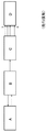
先行技術において周知のような、顕微鏡を制御するための回路が、図1に概略的に示されている。図1の回路は、例えばダブルデータレートランダムアクセスメモリ(DDR−RAM)の形態をした低速メモリを有する。データローダBが、低速メモリAにアドレスを送信して、そのアドレスに記憶された制御情報を要求し、かつ低速メモリAから制御情報を受信する。この制御情報は、高速メモリCに記憶されるが、高速メモリCは、ハードウェアレジスタの形態をしていてもよい。高速メモリCは、典型的には、ラインバッファとして実現される。すなわち、高速メモリCには、試料の照明中に画像ラインにおける全ての画像点用の制御情報が含まれる。高速メモリCに記憶された制御情報は、コントローラDによって検索することができ、かつ顕微鏡を制御するために使用することができる。高速メモリへの書き込みは、原則として、高速メモリが読み出されていない場合にのみ可能である。 A circuit for controlling the microscope, as is well known in the prior art, is schematically shown in FIG. The circuit of FIG. 1 has a low speed memory, for example in the form of a double data rate random access memory (DDR-RAM). The data loader B transmits an address to the low-speed memory A, requests control information stored at the address, and receives control information from the low-speed memory A. This control information is stored in the high-speed memory C, but the high-speed memory C may be in the form of a hardware register. The high speed memory C is typically realized as a line buffer. That is, the high-speed memory C includes control information for all image points in the image line during sample illumination. Control information stored in the high speed memory C can be retrieved by the controller D and used to control the microscope. In principle, writing to the high-speed memory is possible only when the high-speed memory is not read.
1つの画像点用の制御情報には、典型的には複数の要素が含まれる。本出願人によって販売されている共焦点顕微鏡において、64の個別ビットが、1つの画像点用の制御情報として記憶され、コントローラによって評価される。1ビットにより、例えば、照明レーザビームまたは照明レーザラインが、画像点においてオンまたはオフかどうかを制御してもよい。 The control information for one image point typically includes a plurality of elements. In the confocal microscope sold by the applicant, 64 individual bits are stored as control information for one image point and evaluated by the controller. One bit may control, for example, whether the illumination laser beam or illumination laser line is on or off at the image point.
図1に示す回路の動作中に、1つのライン用の制御情報は、2つの画像ラインの活性段階間に低速メモリから高速メモリにロードされる。一般に、照明レーザビームは、走査領域内で、一定の速度で試料にわたって走査される。照明レーザビームが走査領域から出る場合に、照明レーザビームは、減速され、走査領域の初めに対して次の画像ライン上に反対方向に戻る。走査が双方向で実行される場合に、次の画像ラインは、照明レーザビームが試料を横切って戻るときに走査される。走査が一方向の場合に、レーザビームは、オフ状態の間に戻され、方向が変更され、次の画像ラインは、照明レーザビームが戻るまでは走査されない。これは、画像ラインの走査の完了と、照明レーザビームの再配置との間の走査停止に帰着する。これらの走査停止は、制御情報を高速メモリにロードするために用いられる。 During operation of the circuit shown in FIG. 1, control information for one line is loaded from the low speed memory to the high speed memory during the active phase of the two image lines. In general, the illuminating laser beam is scanned across the sample at a constant speed within the scanning region. As the illumination laser beam exits the scan area, the illumination laser beam is decelerated and returns in the opposite direction onto the next image line relative to the beginning of the scan area. If scanning is performed in both directions, the next image line is scanned as the illumination laser beam returns across the sample. If the scan is in one direction, the laser beam is returned during the off state, the direction is changed, and the next image line is not scanned until the illumination laser beam returns. This results in a scan stop between the completion of scanning of the image line and the repositioning of the illumination laser beam. These scan stops are used to load control information into the high speed memory.
先行技術の回路は、大量のデータが、短い期間内に低速メモリから高速メモリにロードされなければならないので、問題がある。この目的のために、回路の個別要素は、ロードされた制御情報が次の画像ラインの初めでアクセスされることになるときにローディング動作が完了しているように、十分に速くなければならない。チャネルによって処理される制御情報が、2進情報であるだけでなく、それどころか数ビットの解像度を有する制御情報であるので、例えば、ロードされるデータ量が増加した場合に、先行技術の回路は働かなくなる。回路の速度をさらに向上させることができないか、向上させるべきでない場合に、走査速度は、低下されなければならない。すなわち、ローディング動作用の時間は、2つの画像ラインにおける走査間のより長い停止によって増加させなければならない。 Prior art circuits are problematic because large amounts of data must be loaded from low speed memory to high speed memory within a short period of time. For this purpose, the individual elements of the circuit must be fast enough so that the loading operation is complete when the loaded control information is to be accessed at the beginning of the next image line. Since the control information processed by the channel is not only binary information, but rather control information with a resolution of several bits, for example, when the amount of data loaded increases, the prior art circuit works. Disappear. If the speed of the circuit cannot be further improved or should not be improved, the scanning speed must be reduced. That is, the time for the loading operation must be increased by a longer pause between scans in the two image lines.
したがって、本発明の目的は、短い期間内に大量のデータを処理し、かつコントローラに利用可能にすることができるような方法で、上記のタイプの回路および方法を改善することである。さらに、本明細書で開示される回路および方法は、できるだけスケーラブルであるべきである。 Accordingly, it is an object of the present invention to improve the above types of circuits and methods in such a way that large amounts of data can be processed and made available to the controller within a short period of time. Furthermore, the circuits and methods disclosed herein should be as scalable as possible.
上記の目的は、本発明の基礎となる概念の実施形態に関する請求項1の特徴により、本発明に従って達成される。したがって、問題の回路は、それが、データローダおよび少なくとも2つの高速メモリを含み、データローダが、低速メモリから少なくとも2つの高速メモリの1つに交互に制御情報が書き込まれるように構成されることと、
回路が、制御情報を読み出すために少なくとも2つの高速メモリの1つにコントローラが交互にアクセスできるようにするマルチプレクサを有することと、
データローダによる書き込み動作およびコントローラによる読み出し動作が、同じ高速メモリに対して同時に行われないような方法でマルチプレクサを制御するように、データローダが構成されることと、を特徴とする。
The above object is achieved according to the invention by the features of
The circuit has a multiplexer that allows the controller to alternately access one of at least two high-speed memories to read control information;
The data loader is configured to control the multiplexer in such a way that the write operation by the data loader and the read operation by the controller are not performed simultaneously on the same high-speed memory.
本発明の基礎となる概念の別の実施形態において、上記の目的は、請求項6の特徴によって達成される。したがって、問題の回路は、m個の別個のデータローダが設けられ、各データローダが、それに関連付けられた高速メモリを有し、1≦m<nであり、データローダのそれぞれが、制御される1つの顕微鏡パラメータに割り当てられることと、
それぞれの高速メモリにロードされる制御情報の部分が、それぞれのデータローダによって制御されることになる顕微鏡パラメータを表す部分であるように、データローダが構成されることと、
回路が、m個の高速メモリに記憶された制御情報をn本のラインを介してコントローラによってアクセスできるようにするスイッチングマトリックスを有することと、を特徴とする。
In another embodiment of the concept underlying the present invention, the above object is achieved by the features of
The data loader is configured such that the portion of the control information loaded into each high speed memory is a portion representing the microscope parameters to be controlled by the respective data loader;
The circuit has a switching matrix that allows control information stored in m high-speed memories to be accessed by a controller via n lines.
方法に関して、上記の目的は、本発明の基礎となる概念の実施形態に関する請求項14の特徴によって達成される。したがって、当該方法には、
データローダによって、低速メモリから制御情報をロードするステップと、
データローダによって、少なくとも2つの高速メモリの1つに制御情報を交互に書き込むステップと、
データローダがそれぞれの高速メモリに同時に書き込まないような方法で、少なくとも2つの高速メモリの1つへの読み出しアクセスがイネーブルされるようにマルチプレクサを切り替えるステップと、
コントローラによって、選択された高速メモリにマルチプレクサを介してアクセスし、かつ記憶された制御情報を読み出すステップと、
読み出した制御情報に基づいて顕微鏡をコントローラによって制御するステップと、が含まれる。
With regard to the method, the above object is achieved by the features of claim 14 relating to the conceptual embodiment underlying the invention. Therefore, the method includes
Loading control information from low-speed memory by a data loader;
Alternately writing control information to one of at least two high-speed memories by a data loader;
Switching the multiplexer to enable read access to one of the at least two high speed memories in such a way that the data loader does not write to each high speed memory simultaneously;
Accessing a selected high-speed memory through a multiplexer and reading stored control information by a controller;
Controlling the microscope with a controller based on the read control information.
本発明の方法の別の実施形態において、上記の目的は、請求項15の特徴によって達成される。したがって、当該方法には、
制御されるm個の顕微鏡パラメータのそれぞれの1つに関する制御情報を、m個の別個のデータローダのそれぞれによってロードするステップと、
それぞれのデータローダに関連付けられた高速メモリに制御情報を、それぞれのデータローダによって書き込むステップと、
高速メモリに記憶された制御情報に、スイッチングマトリックスを介してコントローラによってアクセスするステップと、
スイッチングマトリックスを介して、高速メモリから制御情報をコントローラによって読み出すステップと、
読み出した制御情報に基づき、コントローラによって顕微鏡を制御するステップと、が含まれる。
In another embodiment of the method of the present invention, the above object is achieved by the features of claim 15. Therefore, the method includes
Loading control information for each one of the m microscope parameters to be controlled by each of the m separate data loaders;
Writing control information to the high speed memory associated with each data loader by each data loader;
Accessing control information stored in high-speed memory by a controller via a switching matrix;
Reading control information from the high-speed memory by the controller via the switching matrix;
And controlling the microscope by the controller based on the read control information.
本発明によれば、低速メモリから高速メモリに制御情報をロードするための動作が、複数の高速メモリ間に分散されるという点で、データスループットを改善できることが第1に分かった。したがって、ローディング動作は、最適化され、より効率的に制御することができる。この概念は、本発明の基礎を形成するが、2つの異なる方法で実現することができる。第1に、複数の高速メモリのために1つの共通データローダが働いてもよい。第2に、複数の個別のデータローダを設け、それぞれが、それに関連付けられた高速メモリを有してもよい。 According to the present invention, it was first found that the data throughput can be improved in that the operation for loading control information from the low-speed memory to the high-speed memory is distributed among a plurality of high-speed memories. Thus, the loading operation is optimized and can be controlled more efficiently. This concept forms the basis of the present invention, but can be realized in two different ways. First, one common data loader may work for multiple high speed memories. Second, a plurality of individual data loaders may be provided, each having a high speed memory associated therewith.
第1の実施形態において、回路には、少なくとも2つの高速メモリに通信可能に接続される1つのデータローダが含まれる。データローダは、低速メモリに記憶された制御情報を複数の高速メモリの1つに交互に書き込むように構成される。それぞれの高速メモリに記憶された制御情報が高速メモリから読み出されるように、回路には、制御情報を読み出すためにコントローラが少なくとも2つの高速メモリの1つに交互にアクセスできるようにするマルチプレクサが含まれる。データローダは、データローダによる書き込み動作およびコントローラによる読み出し動作が、同じ高速メモリに対して同時に行われないような方法で、高速メモリおよびマルチプレクサへの書き込み動作を制御する。書き込みおよび読み出し動作を調和させることによって、データローダは、コントローラが、(例えば画像ライン用の)正確な制御情報を読み出し得ること、および制御情報が、単に高速メモリに書き込まれるだけで、一方でコントローラが、この高速メモリからデータを読み出すことができないことを常に保証することができる。したがって、書き込みおよび読み出し動作は、互いに分離され、より長い停止は、制御情報をロードするために使用することができる。また、2つの連続画像ラインの活性段階間の短い期間だけを、制御情報を高速メモリにロードするために使用する代わりに、制御情報は、照明レーザビームを再配置するために、(高速メモリの数に依存して)少なくとも1つの画像ラインを走査するために、および照明レーザビームをさらに再配置するために必要とされる期間中に、高速メモリにロードすることができる。これは、低速メモリを対象にしたロード要求のかなりの分散に帰着する。 In the first embodiment, the circuit includes one data loader communicatively connected to at least two high speed memories. The data loader is configured to alternately write control information stored in the low speed memory to one of the plurality of high speed memories. The circuit includes a multiplexer that allows the controller to alternately access one of the at least two high speed memories to read the control information so that the control information stored in each high speed memory is read from the high speed memory. It is. The data loader controls the writing operation to the high speed memory and the multiplexer in such a way that the writing operation by the data loader and the reading operation by the controller are not performed simultaneously on the same high speed memory. By coordinating write and read operations, the data loader allows the controller to read accurate control information (eg for image lines) and that the control information is simply written to high speed memory while the controller However, it can always be guaranteed that data cannot be read from this high speed memory. Thus, the write and read operations are separated from each other and a longer pause can be used to load control information. Also, instead of using only a short period between the active phases of two consecutive image lines to load the control information into the high-speed memory, the control information is used to relocate the illumination laser beam (of the high-speed memory). Depending on the number (depending on the number), it can be loaded into the high-speed memory during the period required to scan at least one image line and during further repositioning of the illumination laser beam. This results in a considerable distribution of load requests for slow memory.
できるだけ簡単に制御情報にアクセスするために、データローダは、グループ化できる制御情報項目が共通高速メモリに記憶されるような方法で、個別高速メモリへのローディング動作を制御するのが好ましい。これは、例えば、顕微鏡によって走査される画像の1つのライン用の制御情報が、いつでも高速メモリの1つに記憶されるという点で、達成可能である。したがって、第1に、ローディングおよび書き込み動作中のアドレス指定は単純化され、第2に、マルチプレクサは、より低速の回路要素を用いて実現することができ、個別高速メモリ間を非常に高い頻度であちこち切り替わる必要がない。他方で、書き込み動作は、より容易に調和させることができる。なぜなら、データローダが、コントローラによって現在要求されている制御情報に関する詳細情報を有する必要がないからである。 In order to access the control information as simply as possible, the data loader preferably controls the loading operation to the individual high-speed memory in such a way that control information items that can be grouped are stored in the common high-speed memory. This can be achieved, for example, in that control information for one line of the image scanned by the microscope is always stored in one of the high-speed memories. Thus, firstly, addressing during loading and writing operations is simplified, and secondly, multiplexers can be implemented using slower circuit elements and very frequently between individual high speed memories. There is no need to switch around. On the other hand, the write operations can be more easily coordinated. This is because the data loader does not need to have detailed information about the control information currently requested by the controller.
顕微鏡パラメータの要求された設定を定義する制御情報は、顕微鏡によって走査される各画像点用の高速メモリに記憶されるのが好ましい。個別パラメータは、「ON」または「OFF」などの2進情報の形態をしていてもよい。他方で、パラメータ用の制御情報には、数ビットの幅を有する情報項目の形態をした様々な中間状態を含んでもよい。したがって、例えば、4ビットまたは8ビット幅の情報項目を制御情報チャネルに記憶してもよい。原則として、異なるビット幅を有する制御情報項目が、個別チャネルに記憶されることがまた可能である。 Control information defining the required settings of the microscope parameters is preferably stored in a high speed memory for each image point scanned by the microscope. The individual parameter may be in the form of binary information such as “ON” or “OFF”. On the other hand, the control information for parameters may include various intermediate states in the form of information items having a width of several bits. Thus, for example, a 4-bit or 8-bit wide information item may be stored in the control information channel. In principle, it is also possible for control information items with different bit widths to be stored in individual channels.
マルチプレクサのローディング動作およびスイッチングを調和させるために、データローダは、入力部、すなわち、それを介して、走査動作の現在の状態に関する情報がデータローダに転送される入力部を有することが可能である。このようにして、データローダは、画像の初め、画像の終わり、ラインの初め、および/またはラインの終わりを示す情報を受信することが可能である。 In order to coordinate the multiplexer loading operation and switching, the data loader may have an input, ie an input through which information about the current state of the scanning operation is transferred to the data loader. . In this way, the data loader can receive information indicating the beginning of the image, the end of the image, the beginning of the line, and / or the end of the line.
したがって、例えば、ラインの終わりを信号で伝えることによって、データローダは、マルチプレクサによって現在選択されている高速メモリにおける制御情報が、もはや必要とされず、したがって低速メモリからロードされる新しい制御情報によって上書きされてもよいことを通知され得る。ラインの終わりはまた、マルチプレクサが、定義された期間内に、すなわち次の走査ラインが始まるまでの時間内に、別の高速メモリに切り替えられなければならないことを示す。 Thus, for example, by signaling the end of the line, the data loader will no longer require the control information in the high speed memory currently selected by the multiplexer to be overwritten by new control information loaded from the low speed memory. May be notified that it may be. The end of the line also indicates that the multiplexer must be switched to another fast memory within a defined period of time, i.e., the time until the next scan line begins.
ラインの初めを信号で伝えることによって、データローダは、高速メモリ、すなわちマルチプレクサによって現在アドレス指定されている高速メモリは、もはや書き込まれることができないことを示す情報を受信する。その理由は、ラインの初めに、コントローラが、マルチプレクサによって現在アドレス指定されている高速メモリにアクセスし、かつ高速メモリから現在の走査ライン用の制御情報を読み出すからである。回路によって満たされる比較的厳密なリアルタイム要件ゆえに、同時の書き込みおよび読み出し動作は許可されず、データローダは、それぞれの高速メモリにもはや書き込むことができない。 By signaling the beginning of the line, the data loader receives information indicating that the high speed memory, ie the high speed memory currently addressed by the multiplexer, can no longer be written. The reason is that at the beginning of the line, the controller accesses the high speed memory currently addressed by the multiplexer and reads the control information for the current scan line from the high speed memory. Due to the relatively strict real-time requirements met by the circuit, simultaneous write and read operations are not allowed and the data loader can no longer write to the respective high speed memory.
画像の終わりを信号で伝えることによって、データローダは、制御情報が、比較的長い期間にわたりコントローラによって読み出されないことを通知される。この比較的長い期間は、新しい画像の走査が始まる始点への照明レーザビームの移動ゆえである。この期間中に、データローダは、できるだけ多くの制御情報を低速メモリから高速メモリにロードしようと試みることができる。このように、複数のメモリは、画像の走査中に、恐らく連続的に、再び「一杯に満たし」かつ空にすることができる。例えば、画像の走査の終わりごろ、データローダによる高速メモリの充填が、このメモリへのアクセスが開始する直前までに完了しないこと、および複数の高速メモリの全てが、更新された制御情報で満たされるわけではないことが起こり得る。特に3つ以上の高速メモリが用いられる場合に、個別高速メモリが、画像の走査中に「古臭くなる」ことさえ起こり得る。 By signaling the end of the image, the data loader is informed that the control information is not read by the controller for a relatively long period of time. This relatively long period is due to the movement of the illumination laser beam to the starting point at which a new image scan begins. During this period, the data loader can attempt to load as much control information as possible from the slow memory to the fast memory. In this way, the plurality of memories can be “full” and empty again, perhaps continuously, during the scanning of the image. For example, at the end of an image scan, the high speed memory filling by the data loader will not be completed by just before access to this memory begins, and all of the multiple high speed memories will be filled with updated control information. Not necessarily. It can even happen that individual high speed memories are “stale” during image scanning, especially when more than two high speed memories are used.
画像の初めを信号で伝えることによって、データローダは、新しい走査動作が開始されたことを通知され得る。 By signaling the beginning of the image, the data loader can be notified that a new scanning operation has started.
制御される1つの顕微鏡パラメータは、レーザ光源またはレーザ光源のレーザラインであることが好ましい。制御される顕微鏡は、例えば、異なる波長を備えた複数のレーザ光源または複数の異なる波長を備えた1つのレーザ光源を有してもよい。次に、1つのパラメータは、例えば、恐らくどの強度で、1つまたは複数のレーザ光源がオンされるか、または1つのレーザ光源の1つもしくは複数のレーザラインが活性化されるかどうかということになろう。 One microscope parameter to be controlled is preferably a laser light source or a laser line of a laser light source. The controlled microscope may have, for example, multiple laser light sources with different wavelengths or one laser light source with multiple different wavelengths. Next, one parameter is, for example, at what intensity one or more laser light sources are turned on or one or more laser lines of one laser light source are activated. Would.
これは、同様に、本発明の基礎となる概念の第2の実施形態に当てはまる。この第2の実施形態によれば、回路には、高速メモリにそれぞれがアクセスできる複数の別個のデータローダが含まれる。普通の顕微鏡実験のほとんどにおいて、制御情報を介して原則として制御可能なnパラメータの全てが、実際に用いられるわけではない。代わりに、実験中には顕微鏡用のm個のパラメータを制御することで通常は十分である。したがって、制御されるこれらの顕微鏡パラメータのそれぞれに対して、別個のデータローダが、回路において用いられる。したがって、各データローダは、制御される1つの定義可能な顕微鏡パラメータに割り当てられる。データローダへの個別パラメータの割り当ては、実験の初めに柔軟に定義することができる。データローダは、特定のデータローダによって制御される顕微鏡パラメータを表す制御情報の部分だけが、それぞれの高速メモリにロードされるように構成される。このように、情報項目の全セットからm個の情報項目だけがロードされ、その結果、データ量は、低減され、かつまたm個の異なる高速メモリ間に分散される。したがって、複数の高速メモリ間における分散の概念は、本発明の基礎を形成するが、このようにまた実行される。 This applies likewise to the second embodiment of the concept underlying the present invention. According to this second embodiment, the circuit includes a plurality of separate data loaders each capable of accessing a high speed memory. In most common microscope experiments, not all of the n parameters that can be controlled in principle via control information are actually used. Instead, it is usually sufficient to control m parameters for the microscope during the experiment. Thus, a separate data loader is used in the circuit for each of these microscope parameters to be controlled. Each data loader is therefore assigned to one definable microscope parameter to be controlled. The assignment of individual parameters to the data loader can be flexibly defined at the beginning of the experiment. The data loader is configured such that only the portion of the control information representing the microscope parameters controlled by a particular data loader is loaded into the respective high speed memory. In this way, only m information items are loaded from the entire set of information items, so that the amount of data is reduced and also distributed among m different high speed memories. Thus, the concept of distribution among multiple high speed memories forms the basis of the present invention, but is also implemented in this way.
コントローラが、n本のラインを介して制御情報を受信することを期待するので、第2の実施形態の回路には、コントローラが、m個の高速メモリに記憶された制御情報にアクセスできるようにするスイッチングマトリックスが含まれる。したがって、制御情報のローディングは、完全に透明にし、かつまたコントローラにとって非常に柔軟にすることができる。本発明の回路の機能に関して、コントローラは、先行技術の回路と本発明による回路との間のどんな差にも気づくことができない。しかしながら、制御データのローディングが、よりよく構造化された方法で実行されるので、本発明の回路は、著しく一層速く、より柔軟である。 Since the controller expects to receive control information via n lines, the circuit of the second embodiment allows the controller to access control information stored in m high-speed memories. A switching matrix is included. Thus, the loading of control information can be completely transparent and also very flexible for the controller. With regard to the function of the circuit according to the invention, the controller is not aware of any difference between the prior art circuit and the circuit according to the invention. However, the circuit of the present invention is significantly faster and more flexible because the loading of control data is performed in a better structured way.
スイッチングマトリックスの好ましい実施形態において、スイッチングマトリックスをm個の高速メモリの1つに接続するラインは、スイッチングマトリックスによって、コントローラへのn本のラインの1つまたは複数に接続される。このように、m個の制御情報項目は、n制御チャンネルの1つまたは複数へ切り替えることができる。これによって、さらなる柔軟性が追加される。 In a preferred embodiment of the switching matrix, the line connecting the switching matrix to one of the m high-speed memories is connected to one or more of the n lines to the controller by the switching matrix. In this way, m control information items can be switched to one or more of the n control channels. This adds additional flexibility.
スイッチングマトリックスは、プログラム可能であるのが好ましく、その結果、m個の高速メモリの1つへのラインと、コントローラへのn本のラインの1つまたは複数との間の相互接続を変更することができる。したがって、制御されるパラメータは、2つの走査動作間で変更し、かつ特定の実験に適合させることができる。 The switching matrix is preferably programmable so that the interconnection between one line of m high speed memories and one or more of the n lines to the controller is changed. Can do. Thus, the controlled parameters can be changed between two scanning operations and adapted to a particular experiment.
低速メモリへのm個のデータローダによる競合アクセスを制御するために、個別読み出しアクセスを制御するアービタを設けることが可能である。単純な実施形態において、アービタは、個別読み出し要求をキューにおいて整理し、それらを次々に処理することが可能である。したがって、読み出し要求は、全ての以前に受信された読み出し要求が処理されるまで、キューに置かれることになろう。これによって、低速メモリへの多数の同次アクセスを防ぐ、非常に単純な方法が提供される。他方で、アービタは、負荷バランシング戦略を遂行することができ、それによって、低速メモリへのアクセスは、定義されるある優先権に従って制御することができる。 In order to control contention access by m data loaders to the low-speed memory, an arbiter for controlling individual read access can be provided. In a simple embodiment, the arbiter can organize individual read requests in a queue and process them one after another. Thus, read requests will be queued until all previously received read requests are processed. This provides a very simple way to prevent multiple simultaneous accesses to slow memory. On the other hand, the arbiter can perform a load balancing strategy, whereby access to the slow memory can be controlled according to certain defined priorities.
高速メモリにおける制御情報へのコントローラのアクセス用に、32以上のチャネルが設けられるのが好ましい。これによって、n=32ラインを介して、制御情報を受信することが可能になる。特に好ましくは、nは、n≧64として選択され、その結果、64チャネルが、制御情報を受信するために設けられる。特に好ましい実施形態において、74のかかる制御チャンネルが設けられる。 More than 32 channels are preferably provided for controller access to control information in high speed memory. As a result, control information can be received via n = 32 lines. Particularly preferably, n is selected as n ≧ 64, so that 64 channels are provided for receiving control information. In a particularly preferred embodiment, 74 such control channels are provided.
他方でm、すなわち制御されるパラメータの数は、16以上であるように選択されるのが好ましい。特に好ましくは、同時に制御されるパラメータの数は、12以下であり、特に好ましい実施形態において、8以下である。 On the other hand, m, ie the number of parameters to be controlled, is preferably chosen to be 16 or more. Particularly preferably, the number of simultaneously controlled parameters is 12 or less, and in a particularly preferred embodiment is 8 or less.
データローダは、制御情報のローディングが、走査プロセスの活性段階間に行われるように構成してもよい。活性段階は、2つの画像ラインの走査によって生成される。ローディング時間は、画像ラインの走査の終了後にレーザが、次の画像または次の画像ラインを走査するために再配置される期間によって定義される。この時間の間に、高速メモリのどれもアクセスされないことを保証することが可能である。 The data loader may be configured such that the loading of control information occurs during the active phase of the scanning process. The active stage is generated by scanning two image lines. The loading time is defined by the period during which the laser is repositioned to scan the next image or next image line after the end of scanning of the image line. During this time, it is possible to ensure that none of the high speed memory is accessed.
本発明の基礎となる概念の第2の実施形態において、制御される顕微鏡パラメータにはまた、レーザ光源またはレーザ光源のレーザラインを含んでもよい。 In a second embodiment of the concept underlying the present invention, the controlled microscope parameters may also include a laser light source or a laser line of a laser light source.
本発明概念の別の好ましい実施形態において、第1および第2の実施形態を組み合わせてもよい。この実施形態によれば、各データローダは、それに関連付けられた少なくとも2つの高速メモリを有することになり、各データローダは、高速メモリの1つに交互に書き込むように構成される。データローダによって制御されるマルチプレクサは、コントローラが、データローダに関連付けられた少なくとも2つの高速メモリの1つに交互にアクセスできるようにする。そのプロセスにおいて、コントローラは、スイッチングマトリックスおよびマルチプレクサを介して、特定のアドレス指定された高速メモリにアクセスする。データローダは、それぞれのデータローダによる書き込みアクセスおよびコントローラによる読み出しアクセスが、同じ高速メモリに対して同時に行われないような方法で、マルチプレクサを制御するように構成される。したがって、ローディング動作は、さらに最適化することができ、低速メモリは、より効率的に読み出すことができる。 In another preferred embodiment of the inventive concept, the first and second embodiments may be combined. According to this embodiment, each data loader will have at least two high speed memories associated with it, and each data loader is configured to alternately write to one of the high speed memories. A multiplexer controlled by the data loader allows the controller to alternately access one of the at least two high speed memories associated with the data loader. In that process, the controller accesses a specific addressed high-speed memory through the switching matrix and multiplexer. The data loader is configured to control the multiplexer in such a way that write access by each data loader and read access by the controller are not made simultaneously to the same high speed memory. Thus, the loading operation can be further optimized and the low speed memory can be read more efficiently.
本発明の教示は、様々な方法で有利に具体化し改良することが可能である。この点において、一方で請求項1および6に従属する請求項が、他方で図面に触れた本発明の好ましい例示的な実施形態の以下の説明が参照される。図面を参照する本発明の好ましい例示的な実施形態の説明に関連して、教示の一般に好ましい実施形態および改良形態の説明がまた提供される。
The teachings of the present invention can be advantageously embodied and improved in various ways. In this respect, reference is made to the claims subordinate to
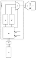
図2は、本発明の両方の態様を組み合わせた、本発明による、顕微鏡を制御するための回路を概略形式で示す。第1に、複数のデータローダが実現され、第2に、各データローダは、それに関連付けられた2つの高速メモリを有する。 FIG. 2 shows in schematic form a circuit for controlling a microscope according to the invention, combining both aspects of the invention. First, multiple data loaders are implemented, and second, each data loader has two high-speed memories associated with it.
図2の回路は、顕微鏡(図示せず)を制御するための制御情報が記憶された低速メモリ1を有する。低速メモリ1は、全ての読み出し要求をキューに入れることによってm個のデータローダ3からの競合アクセスを解決するアービタ2を介してアクセスされる。はっきりさせるために、1つのデータローダ3だけが、関連する要素と共に示されている。しかしながら、破線内の全ての要素は、m回存在し、これらのユニットのそれぞれは、顕微鏡パラメータ用の制御情報にアクセスするように構成される。
The circuit of FIG. 2 has a low-
各データローダ3は、2つの高速メモリ4.1および4.2に接続され、データローダ3は、これらの高速メモリ4.1および4.2に、低速メモリ1からの制御情報を交互に書き込む。2つの高速メモリ4.1および4.2は、今度は、マルチプレクサ5に接続され、マルチプレクサ5は、データローダ3によって制御され、かつ2つの高速メモリ4.1および4.2の1つへの読み出しアクセスを交互に可能にする。m個のデータローダの各1つに接続される全てのm個のマルチプレクサは、スイッチングマトリックス6を介して組み合わされ、制御情報項目は、n出力ラインのいくつかで利用可能にされる。スイッチングマトリックス6の構成は、どの制御情報項目が、n本のラインのどれに存在するかを定義する。単純化された用語では、スイッチングマトリックス6は、m×n本のラインのマトリックスである。個別の交差ライン間の接続が、m個の入力部のどれが、n出力部のどれに適用されるかを定義する。n出力ラインを介して、コントローラ7は、高速メモリ4.1および4.2の1つにおけるm個の顕微鏡パラメータの1つのための制御情報にアクセスすることができる。
Each
データローダは、さらに、2つの入力部8および9を有し、それらを介して、データローダ3には、画像の終わり(入力部8)またはラインの終わり(入力部9)に達したことを通知してもよい。
The data loader further has two
図2の回路の動作中に、m個の顕微鏡パラメータ用の制御情報は、低速メモリ1に記憶される。これに関連して、一方で、メモリは、そこに、制御されるそれぞれのm個のパラメータ用に予め選択された制御情報項目を記憶しておいてもよい。他方で、データローダは、nの可能な制御情報項目の全てから、所望のm個のパラメータ用に必要とされる制御情報項目をフィルタアウトしてもよい。対応する制御情報項目をロードするために、データローダ3は、所望の制御情報項目のアドレスを含む要求をアービタ2に送信し、アービタ2は、その要求をキューに挿入し、かついつでも、最初に受信した要求を低速メモリ1に転送する。低速メモリ1は、要求された制御情報をアービタ2に返し、今度は、アービタ2は、要求しているデータローダ3に受信データを送信する。データローダ3は、受信した制御情報を高速メモリ4.1および4.2の1つに記憶する。
During the operation of the circuit of FIG. 2, control information for m microscope parameters is stored in the
マルチプレクサの出力部で(すなわちスイッチングマトリックス6の方向において)高速メモリ4.2がアクセスされ得るように、データローダ3が、今はマルチプレクサ5を切り替えてあると仮定すると、データローダは、個別制御情報項目を高速メモリ4.1に記憶する。そうする際に、走査される画像のラインにおける各ポイント用に、データローダ3に割り当てられる顕微鏡パラメータを定義する全ての制御情報項目は、高速メモリ4.1に記憶される。ひとたび、それぞれのパラメータ用の全ての制御情報が高速メモリ4.1に記憶されると、データローダ3は、マルチプレクサを切り替える準備ができている。ひとたび入力部9が、走査されるラインの終わりを示す信号を受信すると、データローダ3は、制御信号をマルチプレクサ5に送出し、次に、マルチプレクサ5は、高速メモリ4.1へのアクセスを提供するために、その出力部を切り替える。続いて、データローダ3は、高速メモリ4.2を制御情報で満たすことができる。高速メモリ4.2に既に含まれていたデータは、上書きされる。
Assuming that the
ひとたび入力部8が、画像の終わりを示す信号を受信すると、すなわち、走査動作内の最後のラインおよび最後の画像点が走査されると、データローダは、低速メモリ1からの新しい制御情報で、両方のメモリ4.1および4.2の内容に上書きする。個別データローダー3のバッファリング能力をさらに向上させるために、データローダ3のそれぞれは、追加の高速メモリ4に関連付けてもよい。回路の動作原理は、同じままである。結局、ただ1つの制限要因は、アービタと低速メモリ1との間で利用可能な帯域幅である。しかしながら、利用可能な帯域幅は、はるかに効率的に用いることができる。なぜなら、個別制御情報項目のローディングが、よりよく分散され、かつ今や、帯域幅が、平均で十分である必要があるだけだからである。これは、回路全体によって満たされるリアルタイム要件におけるかなりのシフトに帰着し、スループットは、著しく向上させ最適化することができる。
Once the
本発明による回路および方法のさらなる有利な実施形態に関して、かつ繰り返しを回避するために、説明の一般的部分および添付の特許請求の範囲が参照される。 With regard to further advantageous embodiments of the circuit and method according to the invention and to avoid repetition, reference is made to the general part of the description and the appended claims.
最後に、本発明による回路の上記の例示的な実施形態が、単に、請求される教示を例示するように意図され、その教示をかかる実施形態に限定するように意図されていないことに、特に留意されたい。 Finally, the above-described exemplary embodiments of the circuit according to the present invention are merely intended to illustrate the claimed teachings and not to limit the teachings to such embodiments in particular. Please keep in mind.
A 低速メモリ
B データローダ
C 高速メモリ
D コントローラ
1 低速メモリ
2 アービタ
3 データローダ
4 高速メモリ
5 マルチプレクサ
6 スイッチングマトリックス
7 コントローラ
8 入力部(画像の終わり)
9 入力部(ラインの終わり)
A Low-speed memory B Data loader C High-speed
9 Input section (end of line)
Claims (15)
前記回路が、データローダ(3)と少なくとも2つの高速メモリ(4.1、4.2)とを有し、前記データローダ(3)が、前記低速メモリ(1)から前記少なくとも2つの高速メモリ(4.1、4.2)の1つに交互に前記制御情報が書き込まれるように構成されること、
前記回路が、前記制御情報を読み出すために前記少なくとも2つの高速メモリ(4.1、4.2)の1つに前記コントローラ(7)が交互にアクセスできるようにするマルチプレクサ(5)を有すること、
前記データローダ(3)による書き込み動作および前記コントローラ(7)による読み出し動作が、同じ高速メモリ(4.1、4.2)に対して同時に行われないよう、前記マルチプレクサ(5)を制御するように、前記データローダ(3)が構成されること、を特徴とする制御回路。 A control circuit for controlling a microscope by a controller, the circuit having a low-speed memory (1) for storing control information, wherein the controller (7) sets a microscope parameter based on the control information. In a control circuit configured to control,
The circuit comprises a data loader (3) and at least two high-speed memories (4.1, 4.2), the data loader (3) from the low-speed memory (1) to the at least two high-speed memories The control information is alternately written in one of (4.1, 4.2),
The circuit comprises a multiplexer (5) that allows the controller (7) to alternately access one of the at least two high-speed memories (4.1, 4.2) for reading the control information ,
The multiplexer (5) is controlled so that the write operation by the data loader (3) and the read operation by the controller (7) are not performed simultaneously for the same high-speed memory (4.1, 4.2). And the data loader (3).
m個の別個のデータローダ(3)が設けられ、各データローダ(3)が、それに関連付けられた高速メモリ(4.1、4.2)を有し(1≦m<n)、前記データローダ(3)のそれぞれが、制御されるべき1つの顕微鏡パラメータに割り当てられること、
前記それぞれの高速メモリ(4.1、4.2)にロードされる制御情報の部分が、前記それぞれのデータローダ(3)によって制御されるべき前記顕微鏡パラメータを表す部分であるよう、前記データローダ(3)が構成されること、
前記回路が、前記m個の高速メモリ(4.1、4.2)に記憶された前記制御情報に、n本のラインを介して前記コントローラ(7)によってアクセスできるようにするスイッチングマトリックス(6)を有すること、を特徴とする制御回路。 A control circuit for controlling a microscope by a controller, the circuit having a low-speed memory (1) for storing control information, and the controller (7) controls the control via n lines In a control circuit configured to control a microscope parameter based on the control information so that the information is accessed,
m separate data loaders (3) are provided, each data loader (3) having a high-speed memory (4.1, 4.2) associated with it (1 ≦ m <n), said data That each of the loaders (3) is assigned to one microscope parameter to be controlled,
The data loader so that the part of the control information loaded into the respective high-speed memory (4.1, 4.2) is the part representing the microscope parameters to be controlled by the respective data loader (3) (3) is configured,
A switching matrix (6) enabling the circuit to access the control information stored in the m high-speed memories (4.1, 4.2) by the controller (7) via n lines. A control circuit.
前記回路が、制御情報を読み出すために前記スイッチングマトリックス(6)を介して前記コントローラ(7)が、前記少なくとも2つの高速メモリ(4.1、4.2)の1つに交互にアクセスできるようにするマルチプレクサ(5)を有し、
前記データローダ(3)が、前記データローダ(3)による書き込み動作および前記コントローラ(7)による読み出し動作が同じ高速メモリ(4.1、4.2)に対して同時に行われないよう、前記マルチプレクサを制御するように構成される、請求項6〜11のいずれか一項に記載の制御回路。 Each data loader (3) is connected to at least two high speed memories (4.1, 4.2) and each data loader (3) alternates with one of the high speed memories (4.1, 4.2). Is configured to write to
The circuit allows the controller (7) to alternately access one of the at least two high-speed memories (4.1, 4.2) via the switching matrix (6) to read control information A multiplexer (5)
The multiplexer so that the data loader (3) does not simultaneously perform the write operation by the data loader (3) and the read operation by the controller (7) to the same high-speed memory (4.1, 4.2). 12. A control circuit according to any one of claims 6 to 11 configured to control
前記データローダ(3)によって、低速メモリ(1)から制御情報をロードするステップと、
前記データローダ(3)によって、少なくとも2つの高速メモリ(4.1、4.2)の1つに前記制御情報を交互に書き込むステップと、
前記データローダ(3)が前記それぞれの高速メモリ(4.1、4.2)に同時に書き込まないよう、前記少なくとも2つの高速メモリ(4.1、4.2)の1つへの読み出しアクセスが可能になるようにマルチプレクサ(5)を切り替えるステップと、
選択された高速メモリ(4.1、4.2)に、コントローラ(7)によって前記マルチプレクサ(5)を介してアクセスし、かつ記憶された制御情報を読み出すステップと、
読み出した制御情報に基づいて前記顕微鏡を前記コントローラ(7)によって制御するステップと、を含む制御方法。 A control method for controlling a microscope by a controller,
Loading control information from the low speed memory (1) by the data loader (3);
Alternately writing the control information to one of at least two high-speed memories (4.1, 4.2) by the data loader (3);
Read access to one of the at least two high speed memories (4.1, 4.2) is prevented so that the data loader (3) does not write to the respective high speed memories (4.1, 4.2) simultaneously. Switching the multiplexer (5) to be possible;
Accessing the selected high speed memory (4.1, 4.2) via the multiplexer (5) by the controller (7) and reading the stored control information;
Controlling the microscope with the controller (7) based on the read control information.
制御されるべきm個の顕微鏡パラメータのそれぞれ1つに関する制御情報を、m個の別個のデータローダ(3)のそれぞれによって、ロードするステップと、
前記それぞれのデータローダ(3)に関連付けられた高速メモリ(4.1、4.2)に前記制御情報を、前記それぞれのデータローダ(3)によって書き込むステップと、
前記高速メモリ(4.1、4.2)に記憶された前記制御情報に、スイッチングマトリックス(6)を介してコントローラ(7)によってアクセスするステップと、
前記高速メモリ(4.1、4.2)から前記制御情報を、前記スイッチングマトリックス(6)を介して前記コントローラ(7)によって読み出すステップと、
読み出した制御情報に基づいて、前記顕微鏡を前記コントローラ(7)によって制御するステップと、を含む方法。
A control method for controlling a microscope by a controller,
Loading control information for each one of the m microscope parameters to be controlled by each of the m separate data loaders (3);
Writing the control information to the high speed memory (4.1, 4.2) associated with the respective data loader (3) by the respective data loader (3);
Accessing the control information stored in the high-speed memory (4.1, 4.2) by a controller (7) via a switching matrix (6);
Reading the control information from the high-speed memory (4.1, 4.2) by the controller (7) via the switching matrix (6);
Controlling the microscope with the controller (7) based on the read control information.
Applications Claiming Priority (2)
| Application Number | Priority Date | Filing Date | Title |
|---|---|---|---|
| DE102012208324A DE102012208324B3 (en) | 2012-05-18 | 2012-05-18 | Circuit and method for controlling a microscope |
| DE102012208324.3 | 2012-05-18 |
Publications (2)
| Publication Number | Publication Date |
|---|---|
| JP2013242561A true JP2013242561A (en) | 2013-12-05 |
| JP6364158B2 JP6364158B2 (en) | 2018-07-25 |
Family
ID=49511193
Family Applications (1)
| Application Number | Title | Priority Date | Filing Date |
|---|---|---|---|
| JP2013101048A Expired - Fee Related JP6364158B2 (en) | 2012-05-18 | 2013-05-13 | Circuit and method for controlling a microscope |
Country Status (4)
| Country | Link |
|---|---|
| US (1) | US9612429B2 (en) |
| JP (1) | JP6364158B2 (en) |
| CN (1) | CN103424860B (en) |
| DE (1) | DE102012208324B3 (en) |
Citations (7)
| Publication number | Priority date | Publication date | Assignee | Title |
|---|---|---|---|---|
| JPS57200136A (en) * | 1981-06-01 | 1982-12-08 | Stanford Res Inst Int | Endoscopic method and apparatus including ultrasonic b scanning image treatment |
| JP2003524999A (en) * | 2000-02-23 | 2003-08-19 | サン・マイクロシステムズ・インコーポレイテッド | Method and apparatus for dynamically class-based packet scheduling |
| US20030155494A1 (en) * | 2002-02-20 | 2003-08-21 | Frank Olschewski | Method for user training for a scanning microscope, scanning microscope, and software program for user training for a scanning microscope |
| US20050110994A1 (en) * | 2001-07-23 | 2005-05-26 | Foster Thomas H. | Method for operating a laser scanning confocal microscope system and a system thereof |
| JP2005234435A (en) * | 2004-02-23 | 2005-09-02 | Olympus Corp | Microobservation apparatus, microobservation method and microobservation program |
| JP2008530651A (en) * | 2005-02-08 | 2008-08-07 | エヌエックスピー ビー ヴィ | A low-power register array for high-speed shift operations. |
| JP2009145566A (en) * | 2007-12-13 | 2009-07-02 | Nikon Corp | Laser scanning microscope and scanner driving device |
Family Cites Families (8)
| Publication number | Priority date | Publication date | Assignee | Title |
|---|---|---|---|---|
| JPH05191873A (en) * | 1991-07-31 | 1993-07-30 | Canon Inc | Remote control device |
| US5889982A (en) | 1995-07-01 | 1999-03-30 | Intel Corporation | Method and apparatus for generating event handler vectors based on both operating mode and event type |
| US5889985A (en) * | 1996-08-07 | 1999-03-30 | Elbrus International | Array prefetch apparatus and method |
| US6529510B1 (en) * | 1997-12-19 | 2003-03-04 | Lg Information & Communications, Ltd. | ATM switching apparatus and method thereof |
| US6987561B2 (en) * | 2002-04-24 | 2006-01-17 | Analog Devices, Inc. | System and apparatus for testing a micromachined optical device |
| JP4388318B2 (en) * | 2003-06-27 | 2009-12-24 | オリンパス株式会社 | Image processing device |
| JP2009063637A (en) * | 2007-09-04 | 2009-03-26 | Fujifilm Corp | Optical scanning probe, optical scanning probe device, and optical scanning probe control method |
| CN202133817U (en) * | 2011-07-04 | 2012-02-01 | 上海理工大学 | A multi-channel frequency division multiplexing fluorescence confocal microscopy imaging device |
-
2012
- 2012-05-18 DE DE102012208324A patent/DE102012208324B3/en not_active Expired - Fee Related
-
2013
- 2013-05-13 JP JP2013101048A patent/JP6364158B2/en not_active Expired - Fee Related
- 2013-05-15 US US13/894,503 patent/US9612429B2/en not_active Expired - Fee Related
- 2013-05-17 CN CN201310183408.2A patent/CN103424860B/en active Active
Patent Citations (7)
| Publication number | Priority date | Publication date | Assignee | Title |
|---|---|---|---|---|
| JPS57200136A (en) * | 1981-06-01 | 1982-12-08 | Stanford Res Inst Int | Endoscopic method and apparatus including ultrasonic b scanning image treatment |
| JP2003524999A (en) * | 2000-02-23 | 2003-08-19 | サン・マイクロシステムズ・インコーポレイテッド | Method and apparatus for dynamically class-based packet scheduling |
| US20050110994A1 (en) * | 2001-07-23 | 2005-05-26 | Foster Thomas H. | Method for operating a laser scanning confocal microscope system and a system thereof |
| US20030155494A1 (en) * | 2002-02-20 | 2003-08-21 | Frank Olschewski | Method for user training for a scanning microscope, scanning microscope, and software program for user training for a scanning microscope |
| JP2005234435A (en) * | 2004-02-23 | 2005-09-02 | Olympus Corp | Microobservation apparatus, microobservation method and microobservation program |
| JP2008530651A (en) * | 2005-02-08 | 2008-08-07 | エヌエックスピー ビー ヴィ | A low-power register array for high-speed shift operations. |
| JP2009145566A (en) * | 2007-12-13 | 2009-07-02 | Nikon Corp | Laser scanning microscope and scanner driving device |
Also Published As
| Publication number | Publication date |
|---|---|
| US20130307958A1 (en) | 2013-11-21 |
| JP6364158B2 (en) | 2018-07-25 |
| US9612429B2 (en) | 2017-04-04 |
| CN103424860A (en) | 2013-12-04 |
| CN103424860B (en) | 2017-05-17 |
| DE102012208324B3 (en) | 2013-11-21 |
Similar Documents
| Publication | Publication Date | Title |
|---|---|---|
| JP5504985B2 (en) | Data processing device | |
| CN105320608B (en) | Memory controller and method for controlling a memory device to process access requests | |
| US6002412A (en) | Increased performance of graphics memory using page sorting fifos | |
| JP5841142B2 (en) | System and method for allocating parts of a shared stack | |
| JP6254603B2 (en) | Message signal interrupt communication | |
| JP2002500395A (en) | Optimal multi-channel storage control system | |
| JP5552692B2 (en) | Multimode accessible storage device | |
| US10042773B2 (en) | Advance cache allocator | |
| US20170168723A1 (en) | Host interface controller and control method for storage device | |
| JP6364158B2 (en) | Circuit and method for controlling a microscope | |
| US7664922B2 (en) | Data transfer arbitration apparatus and data transfer arbitration method | |
| US8261023B2 (en) | Data processor | |
| KR102408350B1 (en) | Memory controller of graphic processing unit capable of improving energy efficiency and method for controlling memory thereof | |
| US7047391B2 (en) | System and method for re-ordering memory references for access to memory | |
| US7725623B2 (en) | Command transfer controlling apparatus and command transfer controlling method | |
| US20140204108A1 (en) | Pixel cache, method of operating pixel cache, and image processing device including pixel cache | |
| TWI354252B (en) | Liquid crystal display, timing controller thereof | |
| JPH10157218A5 (en) | ||
| GB2538605B (en) | Digital display | |
| US20050038961A1 (en) | Cache and memory architecture for fast program space access | |
| US8943228B2 (en) | Peripheral interface, data stream, and data transfer method | |
| KR100674712B1 (en) | Scanning system or method of data using DDR | |
| JP4776742B1 (en) | Semiconductor memory device and control method thereof | |
| CN121414945A (en) | A GPU fragment stream processing method | |
| JP2009182438A (en) | Reconfigurable logic circuit device and circuit switching control method |
Legal Events
| Date | Code | Title | Description |
|---|---|---|---|
| A621 | Written request for application examination |
Free format text: JAPANESE INTERMEDIATE CODE: A621 Effective date: 20160506 |
|
| A977 | Report on retrieval |
Free format text: JAPANESE INTERMEDIATE CODE: A971007 Effective date: 20170217 |
|
| A131 | Notification of reasons for refusal |
Free format text: JAPANESE INTERMEDIATE CODE: A131 Effective date: 20170404 |
|
| A601 | Written request for extension of time |
Free format text: JAPANESE INTERMEDIATE CODE: A601 Effective date: 20170703 |
|
| A521 | Request for written amendment filed |
Free format text: JAPANESE INTERMEDIATE CODE: A523 Effective date: 20170901 |
|
| A131 | Notification of reasons for refusal |
Free format text: JAPANESE INTERMEDIATE CODE: A131 Effective date: 20171031 |
|
| A521 | Request for written amendment filed |
Free format text: JAPANESE INTERMEDIATE CODE: A523 Effective date: 20180126 |
|
| TRDD | Decision of grant or rejection written | ||
| A01 | Written decision to grant a patent or to grant a registration (utility model) |
Free format text: JAPANESE INTERMEDIATE CODE: A01 Effective date: 20180605 |
|
| A61 | First payment of annual fees (during grant procedure) |
Free format text: JAPANESE INTERMEDIATE CODE: A61 Effective date: 20180702 |
|
| R150 | Certificate of patent or registration of utility model |
Ref document number: 6364158 Country of ref document: JP Free format text: JAPANESE INTERMEDIATE CODE: R150 |
|
| R250 | Receipt of annual fees |
Free format text: JAPANESE INTERMEDIATE CODE: R250 |
|
| R250 | Receipt of annual fees |
Free format text: JAPANESE INTERMEDIATE CODE: R250 |
|
| R250 | Receipt of annual fees |
Free format text: JAPANESE INTERMEDIATE CODE: R250 |
|
| R250 | Receipt of annual fees |
Free format text: JAPANESE INTERMEDIATE CODE: R250 |
|
| LAPS | Cancellation because of no payment of annual fees |