JP2013242588A - Optical shutter for miniature camera - Google Patents
Optical shutter for miniature camera Download PDFInfo
- Publication number
- JP2013242588A JP2013242588A JP2013149587A JP2013149587A JP2013242588A JP 2013242588 A JP2013242588 A JP 2013242588A JP 2013149587 A JP2013149587 A JP 2013149587A JP 2013149587 A JP2013149587 A JP 2013149587A JP 2013242588 A JP2013242588 A JP 2013242588A
- Authority
- JP
- Japan
- Prior art keywords
- fluid
- shutter
- effective area
- interface
- operating state
- Prior art date
- Legal status (The legal status is an assumption and is not a legal conclusion. Google has not performed a legal analysis and makes no representation as to the accuracy of the status listed.)
- Pending
Links
- 230000003287 optical effect Effects 0.000 title claims abstract description 41
- 239000012530 fluid Substances 0.000 claims description 200
- 230000008859 change Effects 0.000 claims description 12
- 230000005540 biological transmission Effects 0.000 claims description 7
- 238000000034 method Methods 0.000 claims description 6
- 230000003213 activating effect Effects 0.000 claims description 4
- 239000007788 liquid Substances 0.000 abstract description 6
- 238000010586 diagram Methods 0.000 description 19
- 230000005684 electric field Effects 0.000 description 13
- 239000007789 gas Substances 0.000 description 4
- ZWEHNKRNPOVVGH-UHFFFAOYSA-N 2-Butanone Chemical compound CCC(C)=O ZWEHNKRNPOVVGH-UHFFFAOYSA-N 0.000 description 3
- CSCPPACGZOOCGX-UHFFFAOYSA-N Acetone Chemical compound CC(C)=O CSCPPACGZOOCGX-UHFFFAOYSA-N 0.000 description 3
- 230000006870 function Effects 0.000 description 3
- VLKZOEOYAKHREP-UHFFFAOYSA-N n-Hexane Chemical compound CCCCCC VLKZOEOYAKHREP-UHFFFAOYSA-N 0.000 description 3
- VYPSYNLAJGMNEJ-UHFFFAOYSA-N silicon dioxide Inorganic materials O=[Si]=O VYPSYNLAJGMNEJ-UHFFFAOYSA-N 0.000 description 3
- 125000006850 spacer group Chemical group 0.000 description 3
- XKRFYHLGVUSROY-UHFFFAOYSA-N Argon Chemical compound [Ar] XKRFYHLGVUSROY-UHFFFAOYSA-N 0.000 description 2
- IJGRMHOSHXDMSA-UHFFFAOYSA-N Atomic nitrogen Chemical compound N#N IJGRMHOSHXDMSA-UHFFFAOYSA-N 0.000 description 2
- FAPWRFPIFSIZLT-UHFFFAOYSA-M Sodium chloride Chemical compound [Na+].[Cl-] FAPWRFPIFSIZLT-UHFFFAOYSA-M 0.000 description 2
- 230000008901 benefit Effects 0.000 description 2
- 230000015556 catabolic process Effects 0.000 description 2
- 230000008878 coupling Effects 0.000 description 2
- 238000010168 coupling process Methods 0.000 description 2
- 238000005859 coupling reaction Methods 0.000 description 2
- JHIVVAPYMSGYDF-UHFFFAOYSA-N cyclohexanone Chemical compound O=C1CCCCC1 JHIVVAPYMSGYDF-UHFFFAOYSA-N 0.000 description 2
- 238000005516 engineering process Methods 0.000 description 2
- 239000012528 membrane Substances 0.000 description 2
- LQNUZADURLCDLV-UHFFFAOYSA-N nitrobenzene Chemical compound [O-][N+](=O)C1=CC=CC=C1 LQNUZADURLCDLV-UHFFFAOYSA-N 0.000 description 2
- XUIMIQQOPSSXEZ-UHFFFAOYSA-N Silicon Chemical compound [Si] XUIMIQQOPSSXEZ-UHFFFAOYSA-N 0.000 description 1
- 238000010521 absorption reaction Methods 0.000 description 1
- 239000000853 adhesive Substances 0.000 description 1
- 230000001070 adhesive effect Effects 0.000 description 1
- 230000002411 adverse Effects 0.000 description 1
- 239000003570 air Substances 0.000 description 1
- 150000001335 aliphatic alkanes Chemical class 0.000 description 1
- -1 alkanes (eg hexane) Chemical class 0.000 description 1
- 230000003321 amplification Effects 0.000 description 1
- 239000007798 antifreeze agent Substances 0.000 description 1
- 229910052786 argon Inorganic materials 0.000 description 1
- 238000003491 array Methods 0.000 description 1
- 230000002238 attenuated effect Effects 0.000 description 1
- 230000006399 behavior Effects 0.000 description 1
- 230000015572 biosynthetic process Effects 0.000 description 1
- 239000003990 capacitor Substances 0.000 description 1
- 238000006243 chemical reaction Methods 0.000 description 1
- 239000011248 coating agent Substances 0.000 description 1
- 238000000576 coating method Methods 0.000 description 1
- 230000000295 complement effect Effects 0.000 description 1
- 238000005260 corrosion Methods 0.000 description 1
- 230000007797 corrosion Effects 0.000 description 1
- 230000000694 effects Effects 0.000 description 1
- 239000000945 filler Substances 0.000 description 1
- 239000004811 fluoropolymer Substances 0.000 description 1
- 229920002313 fluoropolymer Polymers 0.000 description 1
- 239000011521 glass Substances 0.000 description 1
- 229930195733 hydrocarbon Natural products 0.000 description 1
- 150000002430 hydrocarbons Chemical class 0.000 description 1
- 238000003384 imaging method Methods 0.000 description 1
- AMGQUBHHOARCQH-UHFFFAOYSA-N indium;oxotin Chemical compound [In].[Sn]=O AMGQUBHHOARCQH-UHFFFAOYSA-N 0.000 description 1
- 150000002576 ketones Chemical class 0.000 description 1
- 239000000463 material Substances 0.000 description 1
- 229910044991 metal oxide Inorganic materials 0.000 description 1
- 150000004706 metal oxides Chemical class 0.000 description 1
- 238000012986 modification Methods 0.000 description 1
- 230000004048 modification Effects 0.000 description 1
- 150000002828 nitro derivatives Chemical class 0.000 description 1
- 229910052757 nitrogen Inorganic materials 0.000 description 1
- LYGJENNIWJXYER-UHFFFAOYSA-N nitromethane Chemical compound C[N+]([O-])=O LYGJENNIWJXYER-UHFFFAOYSA-N 0.000 description 1
- VLZLOWPYUQHHCG-UHFFFAOYSA-N nitromethylbenzene Chemical compound [O-][N+](=O)CC1=CC=CC=C1 VLZLOWPYUQHHCG-UHFFFAOYSA-N 0.000 description 1
- 238000003199 nucleic acid amplification method Methods 0.000 description 1
- 238000012634 optical imaging Methods 0.000 description 1
- 230000035699 permeability Effects 0.000 description 1
- 239000000049 pigment Substances 0.000 description 1
- 239000004033 plastic Substances 0.000 description 1
- 239000004417 polycarbonate Substances 0.000 description 1
- 229920000515 polycarbonate Polymers 0.000 description 1
- 239000010970 precious metal Substances 0.000 description 1
- 239000010453 quartz Substances 0.000 description 1
- 238000001454 recorded image Methods 0.000 description 1
- 238000002310 reflectometry Methods 0.000 description 1
- 239000005871 repellent Substances 0.000 description 1
- 239000012266 salt solution Substances 0.000 description 1
- 239000004065 semiconductor Substances 0.000 description 1
- 229910052710 silicon Inorganic materials 0.000 description 1
- 239000010703 silicon Substances 0.000 description 1
- 239000000377 silicon dioxide Substances 0.000 description 1
- 229920002545 silicone oil Polymers 0.000 description 1
- 239000011780 sodium chloride Substances 0.000 description 1
- 239000000243 solution Substances 0.000 description 1
- 238000009736 wetting Methods 0.000 description 1
Images






Classifications
-
- G—PHYSICS
- G03—PHOTOGRAPHY; CINEMATOGRAPHY; ANALOGOUS TECHNIQUES USING WAVES OTHER THAN OPTICAL WAVES; ELECTROGRAPHY; HOLOGRAPHY
- G03B—APPARATUS OR ARRANGEMENTS FOR TAKING PHOTOGRAPHS OR FOR PROJECTING OR VIEWING THEM; APPARATUS OR ARRANGEMENTS EMPLOYING ANALOGOUS TECHNIQUES USING WAVES OTHER THAN OPTICAL WAVES; ACCESSORIES THEREFOR
- G03B9/00—Exposure-making shutters; Diaphragms
- G03B9/08—Shutters
-
- G—PHYSICS
- G02—OPTICS
- G02B—OPTICAL ELEMENTS, SYSTEMS OR APPARATUS
- G02B26/00—Optical devices or arrangements for the control of light using movable or deformable optical elements
- G02B26/004—Optical devices or arrangements for the control of light using movable or deformable optical elements based on a displacement or a deformation of a fluid
-
- H—ELECTRICITY
- H04—ELECTRIC COMMUNICATION TECHNIQUE
- H04N—PICTORIAL COMMUNICATION, e.g. TELEVISION
- H04N23/00—Cameras or camera modules comprising electronic image sensors; Control thereof
- H04N23/50—Constructional details
- H04N23/55—Optical parts specially adapted for electronic image sensors; Mounting thereof
-
- G—PHYSICS
- G02—OPTICS
- G02B—OPTICAL ELEMENTS, SYSTEMS OR APPARATUS
- G02B6/00—Light guides; Structural details of arrangements comprising light guides and other optical elements, e.g. couplings
- G02B6/24—Coupling light guides
- G02B6/26—Optical coupling means
- G02B6/35—Optical coupling means having switching means
- G02B6/3538—Optical coupling means having switching means based on displacement or deformation of a liquid
Landscapes
- Physics & Mathematics (AREA)
- General Physics & Mathematics (AREA)
- Engineering & Computer Science (AREA)
- Multimedia (AREA)
- Signal Processing (AREA)
- Optics & Photonics (AREA)
- Mechanical Light Control Or Optical Switches (AREA)
- Shutters For Cameras (AREA)
- Studio Devices (AREA)
Abstract
Description
本発明は、カメラなどの光学的画像装置における露光時間の制御に関する。 The present invention relates to exposure time control in an optical image device such as a camera.
デジタルカメラは、被写体の画像を画像センサー上に焦点合わせするように構成された画像光学系を備える。画像センサーは、感光性画素の配列を備える。個々の画素からの複数の信号が、被写体の画像を形成する。第一近似として、個々の画素から供給される信号は、前記画素をリセットまたは活性化してから上記信号(例、電荷)をシフトレジスタまたはメモリにシフトするまでの時間の長さに比例する。 The digital camera includes an image optical system configured to focus an image of a subject on an image sensor. The image sensor includes an array of photosensitive pixels. Multiple signals from individual pixels form an image of the subject. As a first approximation, the signal supplied from each pixel is proportional to the length of time from resetting or activating the pixel to shifting the signal (eg, charge) to a shift register or memory.
典型的な低価格の画像センサーは電荷シフトレジスタを備えないため、信号を取り込み、保持することができない。このため、全信号の読み込みが、同時にできないときに、個々の画素から得られた信号は、異なる時間間隔に対応してしまう。これは、特にカメラまたは被写体が動くとき、記録画像の歪みや画像の不自然さ(artifact)の原因となる場合がある。 A typical low cost image sensor does not include a charge shift register and therefore cannot capture and hold a signal. For this reason, when all the signals cannot be read simultaneously, the signals obtained from the individual pixels correspond to different time intervals. This can cause recorded image distortion and image artifacts, especially when the camera or subject moves.
この問題は、いわゆる全面同時シャッターを用いて全ての画素の露光を実質的に同時に制御することにより修正できる場合がある。全面同時シャッターが閉じた後における個々の画素からの信号は、実質的に一定状態で維持され、各画素の電気的な読取が同時に行われない場合においても、得られる画像は同時露光に相当する。 This problem may be corrected by controlling exposure of all pixels substantially simultaneously using a so-called full-surface simultaneous shutter. The signals from the individual pixels after the full-surface simultaneous shutter is closed are maintained in a substantially constant state, and the obtained image corresponds to simultaneous exposure even when electrical reading of each pixel is not performed simultaneously. .
しかしながら、従来の機械的グローバル・シャッターは、例えば、複雑な機械構造、大きなサイズ、および消費電力が比較的大きいなど、いくつかの欠点がある。従って機械的に組み込まれた全面同時シャッター(グローバル・シャッター)は、小型携帯型装置に一体化される画像システムとしては好適ではない。 However, conventional mechanical global shutters have several drawbacks, such as complex mechanical structures, large sizes, and relatively high power consumption. Therefore, a mechanically incorporated full-surface simultaneous shutter (global shutter) is not suitable as an image system integrated with a small portable device.
米国特許第4,249,814号は、カメラフィルムへの光透過の制御手段として全内部反射原理を用いたカメラシャッターを開示している。このシャッターは、少なくとも二つのプリズム要素を備える。これらのプリズム間の間隙を機械的に開閉して、全内部反射を、有効または無効にする。 U.S. Pat. No. 4,249,814 discloses a camera shutter that uses the total internal reflection principle as a means of controlling light transmission to the camera film. This shutter comprises at least two prism elements. The gap between these prisms is mechanically opened and closed to enable or disable total internal reflection.
米国特許第6,377,383号は、全内部反射に基づく光学スイッチを開示する。皮膜のような補強された表面部が液中に懸下される。この補強された表面部が、静電的に動作して、界面における全内部反射を有効または無効にする。 US Pat. No. 6,377,383 discloses an optical switch based on total internal reflection. A reinforced surface such as a film is suspended in the liquid. This reinforced surface acts electrostatically to enable or disable total internal reflection at the interface.
米国特許第4,701,021号は、光束の減衰を制御するための光束強度変調装置を開示する。この変調装置は、二つのプリズムの間に毛細空間を備える。一定量の流体が、毛細空間内を静電的に移動して、上記流体と上記毛細空間の壁との間の界面における全内部反射を有効または無効にする。毛細空間から流体を取り除いて全内部反射が有効になった際、反射光は吸収用スクリーンに向けられ、光の透過部分は実質的に減衰される。 U.S. Pat. No. 4,701,021 discloses a beam intensity modulator for controlling the attenuation of a beam. This modulation device includes a capillary space between two prisms. A certain amount of fluid moves electrostatically in the capillary space to enable or disable total internal reflection at the interface between the fluid and the wall of the capillary space. When fluid is removed from the capillary space and total internal reflection is enabled, the reflected light is directed to the absorbing screen and the light transmission is substantially attenuated.
本発明の目的は、光学的画像システムの露光を制御するためのシャッターおよび方法を提供することにある。本発明のもう一つの目的は、上記シャッターを備える光学装置を提供することにある。 It is an object of the present invention to provide a shutter and method for controlling the exposure of an optical imaging system. Another object of the present invention is to provide an optical device including the shutter.
本発明の第一の態様によれば、
透明体と毛細空間との間の界面と、
少なくとも一つの流体容器と、
一定量の流体と、
上記流体容器と上記毛細空間との間で前記流体を移動させ、上記界面の有効領域に作用(impinge on)する傾斜光線の全内部反射が可能とするシャッターの第一動作状態と、上記界面の有効領域を通じて上記傾斜光線が透過することを可能とするシャッターの第二動作状態との間で変化を起こさせるための流体移動手段と、
上記毛細空間に上記流体を供給するための上記有効領域に対向する一つ以上の流体ダクトと、
上記界面の有効領域を通じて透過した光線を吸収するための吸収手段と、を備える光学シャッターが提供される。
According to the first aspect of the present invention,
An interface between the transparent body and the capillary space;
At least one fluid container;
A certain amount of fluid,
A first operating state of the shutter that moves the fluid between the fluid container and the capillary space and allows total internal reflection of inclined rays that impinge on the effective area of the interface; Fluid moving means for causing a change between a second operating state of the shutter that allows the tilted rays to pass through the effective area;
One or more fluid ducts facing the effective area for supplying the fluid to the capillary space;
There is provided an optical shutter comprising absorbing means for absorbing light transmitted through the effective area of the interface.
本発明の第二の態様による光学装置は、
画像光学系と、画像センサーと、光学シャッターとを備え、
上記光学シャッターは、同様に
透明体と毛細空間との間の界面と、
少なくとも一つの流体容器と、
一定量の流体と、
上記流体容器と上記毛細空間との間で上記流体を移動させ、上記界面の有効領域に作用する傾斜光線の全内部反射を可能とするシャッターの第一動作状態と、上記界面の有効領域を通じて上記傾斜光線が透過することを可能とするシャッターの第二動作状態との間で変化を起こさせるための流体移動手段と、
上記毛細空間に上記流体を供給するための上記有効領域に対向する一つ以上の流体ダクトと、
上記界面の有効領域を通じて透過する光線を吸収するための吸収手段と、を含む。
The optical device according to the second aspect of the present invention comprises:
An image optical system, an image sensor, and an optical shutter;
Similarly, the optical shutter has an interface between the transparent body and the capillary space,
At least one fluid container;
A certain amount of fluid,
A first operating state of the shutter that moves the fluid between the fluid container and the capillary space and enables total internal reflection of the inclined light rays acting on the effective area of the interface, and through the effective area of the interface Fluid moving means for causing a change between a second operating state of the shutter that allows transmission of tilted rays;
One or more fluid ducts facing the effective area for supplying the fluid to the capillary space;
Absorbing means for absorbing light transmitted through the effective area of the interface.
本発明の第三の態様によれば、透明体と毛細空間との間の界面を備えるシャッターによって、画像センサーの露光を制御する方法が提供され、上記方法は、
ある斜角で、上記界面の有効領域に光線を案内すること、
上記界面の有効領域に作用する傾斜光線の全内部反射を可能とする前記シャッターの第一動作状態と、上記傾斜光線の上記界面における上記有効領域を通じた透過を可能とする上記シャッターの第二動作状態との間で変化を起こさせるように、上記有効領域に対向する少なくとも一つの流体ダクトにおいて、一つ以上の上記流体ダクトを通じて、少なくとも一つの流体容器と上記毛細空間との間で一定量の流体を移動させること、
上記有効領域を透過した光線を吸収すること、および
上記第一動作状態において、上記有効領域から反射された光線を上記画像センサーに案内すること、を含む。
According to a third aspect of the present invention, there is provided a method for controlling exposure of an image sensor with a shutter having an interface between a transparent body and a capillary space, the method comprising:
Guiding the light beam to the effective area of the interface at an oblique angle;
A first operating state of the shutter that allows total internal reflection of tilted light rays acting on an effective area of the interface, and a second operation of the shutter that allows transmission of the tilted light rays through the effective area at the interface. A constant amount between at least one fluid container and the capillary space through the one or more fluid ducts in at least one fluid duct facing the effective area so as to cause a change between states. Moving the fluid,
Absorbing the light beam transmitted through the effective region, and guiding the light beam reflected from the effective region to the image sensor in the first operation state.
界面の有効領域に導入される傾斜光線は、毛細空間が例えば気体など低屈折率を有する媒体で満たされた際に全内部反射によって反射される。反射光はその後、画像光学系を介して画像センサーに案内され、被写体のデジタル画像を結ぶ。従って、画像センサーの露光はシャッターの状態を変化させることによって制御することができる。シャッターは、高屈折率を有する流体で毛細空間を急速に満たすことで無反射状態に設定される。この結果、光線の全内部反射は妨げられ、すなわち無効になる。無反射状態では、光線は、界面の有効領域を通じて透過し、流体および/または毛細空間の対向する表面に吸収される。 The inclined light beam introduced into the effective area of the interface is reflected by total internal reflection when the capillary space is filled with a medium having a low refractive index such as gas. The reflected light is then guided to the image sensor via the image optical system and forms a digital image of the subject. Therefore, the exposure of the image sensor can be controlled by changing the state of the shutter. The shutter is set in a non-reflective state by rapidly filling the capillary space with a fluid having a high refractive index. As a result, the total internal reflection of the light rays is prevented, i.e. is ineffective. In the non-reflective state, light rays are transmitted through the effective area of the interface and absorbed by the opposing surfaces of the fluid and / or the capillary space.
流体は、界面の有効領域に対向する少なくとも一つの流体ダクトを通じて、毛細空間に導入される。流体ダクトは有効領域に対向するため、有効領域を完全に覆うための流体の移動距離は、有効領域の幅よりも実質的に短い。これによってシャッターの動作速度が向上する。 Fluid is introduced into the capillary space through at least one fluid duct facing the effective area of the interface. Since the fluid duct faces the effective area, the moving distance of the fluid for completely covering the effective area is substantially shorter than the width of the effective area. This improves the operating speed of the shutter.
一実施形態において、シャッターは、シャッター動作速度の向上および/または広い有効領域確保のために、いくつかの隣接する流体ダクトをさらに備えることが可能である。 In one embodiment, the shutter can further comprise several adjacent fluid ducts to increase shutter operating speed and / or to secure a large effective area.
一実施形態における流体は、静電引力および/または圧電ポンプによって移動させることが可能である。 The fluid in one embodiment can be moved by electrostatic attraction and / or a piezoelectric pump.
画像を形成する光線は毛細空間を通過しないため、得られる画像の歪みを最小化できる。光線の方向は、全内部反射によって変化するため、光学システムのコンパクト化とスリム化を可能にする。反射光のみが画像化目的に使用されるため、シャッター背面の空間を携帯機器の他の部品のために使用することができる。流体の移動質量は非常に小さく、従って、シャッター動作中の振動や雑音が低い。また、電力消費量も非常に少ない。 Since the light rays forming the image do not pass through the capillary space, distortion of the obtained image can be minimized. Since the direction of the light beam is changed by total internal reflection, the optical system can be made compact and slim. Since only the reflected light is used for imaging purposes, the space behind the shutter can be used for other parts of the portable device. The moving mass of the fluid is very small and therefore has low vibration and noise during shutter operation. In addition, power consumption is very low.
本発明の実施形態およびその利点は、下記の記述および例、ならびに添付の請求範囲によって当業者により明らかになるであろう。 Embodiments of the present invention and advantages thereof will be apparent to those skilled in the art from the following description and examples, and from the appended claims.
以下の実施例では、添付図を参照しながら本発明の実施形態を詳細に記述する。 The following examples describe embodiments of the present invention in detail with reference to the accompanying drawings.
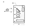
図1に示す光学装置500は画像システムを備える。画像システムは、被写体900の画像を形成するために、被写体900から画像センサー200へ到達する光線B1を焦点合わせするように構成された画像光学系300を備える。画像センサー200の露光は、シャッター100により少なくとも部分的に画定される。
The
シャッター100が反射状態にある場合、反射光B2は画像光学系300を通じて画像センサー200に案内される。シャッター100が無反射状態にある場合、光線B1はシャッター100に吸収される。
When the
画像動作は、少なくとも部分的には制御装置400によって制御され、この制御装置が、直接的または間接的に、画像光学系300、シャッター100および画像センサー200の焦点動作や絞り動作を制御する。装置500は、シャッター100に送信される信号の電圧増幅および/またはデジタル・アナログ変換を行う駆動装置420をさらに備える場合もある。
The image operation is controlled at least in part by the
画像光学系300をシャッター100の前に配置してもよい。画像光学系300の個々の要素をシャッター100の前と後の両方に配置してもよい。
The image
光線B1はシャッター100に反射するため、光学装置500は非常に細くすることができ、即ち寸法D5を小さくすることができる。入射光B1と反射光B2との間の角度は実質的に90度としてもよい。
Since the light beam B1 is reflected by the
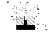
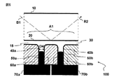
図2は、反射状態にあるシャッター100を示す。光線B1は、実質的な透明体10を通じて、透明体10と毛細空間30との間にある界面20に案内される。毛細空間30は、透明体10よりも低い屈折率を有する第二流体15で満たされている。光線B1は、界面20の法線N1に対し斜角αで界面20に導入される。入射光B1の入射角α、透明体10の屈折率および第二流体15の屈折率は、光線B1が全内部反射により界面20の有効領域A1から反射されるように選択される。反射光B2は、画像センサー200(図1参照)に案内される。第二流体15の屈折率を最小化するため、第二流体15には例えば気体などを用いる。
FIG. 2 shows the
また、シャッター100は、第一流体50を収める少なくとも一つの流体容器70と、少なくとも一つの流体ダクト40と、流体移動手段60と、を備える。第一流体50は、第二流体15よりも高い屈折率を有するように選定する。第一流体15は、例えば液体でもよい。第一流体50と第二流体15とは、相互に非混和になるように選定される。
The
透明体10はガラス、石英、またはポリカーボネートなどのプラスチックでもよい。
The
図3に示すように、シャッター100は、流体移動手段60によって第一流体50を移動させることにより無反射状態に設定することができ、第一流体50は、界面20に作用しながら空洞30内に広がる。
As shown in FIG. 3, the
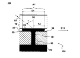
図4は無反射状態のシャッター、すなわち内部反射が妨げられた状態のシャッター100を示す。第一流体50の屈折率は、入射光B1に対する全内部反射の基準を満たさないよう、第二流体15の屈折率よりも大きくなっている。従って、光線B1は、界面20を透過し、吸収面99および/または第一流体50によって吸収される。第一流体50は、光線B1を吸収する色素を含んでもよい。
FIG. 4 shows the
光線B1が有効領域A1で反射されないように、第一流体50の屈折率を、第二流体40よりも実質的に大きな屈折率に選定する。図2と同様に、同一入射角αを仮定する。第一流体50の屈折率は、透明体10の屈折率と実質的に等しくてもよい。
The refractive index of the
有効領域A1は、界面20内の領域であって、この領域を第一流体50で完全に覆うことにより無反射状態に設定することができ、この領域を第二流体15で完全に覆うことにより反射状態に設定することができる。有効領域A1は、光線B1の入射角に依存する。
The effective area A1 is an area in the
全内部反射のための光線の最小角は、透明体10と第二流体15との間の屈折率の差に依存する。内部反射を妨げる最大角は、透明体10と第一流体50との間の屈折率の差に依存する。したがって、第一流体50の屈折率と第二流体15の屈折率との間の差を最大化することは、シャッター100の視野を最大にすることであり、すなわち有効領域A1が反射状態と無反射状態との間で変化するときの角度αの広がりを最大にすることになる。
The minimum ray angle for total internal reflection depends on the difference in refractive index between the
シャッター100は、有効領域A1に対向する一つ以上の流体ダクト40を備える。このため、流体最前部がS1X方向とS1Xと反対の方向に移動する横方向距離D2は、有効領域A1の幅D1よりも実質的に短い。この結果、シャッターの動作速度は、第一流体50が有効領域A1の端部まで導入される仮想的なシャッターよりも実質的に速くなる。流体ダクト40の向きは、有効領域A1に実質的に対して直交してもよい。少なくとも一つの流体ダクト40は、有効領域A1の中心または中央部に対向してもよい。
The
全内部反射を用いる方法は、毛細空間30の厚さが光線B1の波長より実質的に大きいことを必要とする。この厚さは、例えば1μm以上である。厚さを薄くすることは、第一流体50の移動体積を小さくすることに相当する。しかしながら、毛細空間をより厚くすること、たとえば100μmの厚さにすることは、流動抵抗を減少させることになる。
The method using total internal reflection requires that the thickness of the
シャッター100を密封すると有利である。圧力上昇を防ぐために、第二流体15が毛管空間30を流入/流出できるようなダクトは、一つ以上あってもよい(図12または図19を参照)。
It is advantageous to seal the
第一流体50による界面20の濡れを最小化するため、第一流体50の表面張力は、界面20および吸収面99の臨界表面張力よりも大きくしてもよい。このようにすると、これらの表面は第一流体50をはじくことになる。このことは、毛管空間30内の第一流体50の形状を壊れにくく安定に維持することを容易にする。臨界表面張力を改良するため、界面等の表面を、たとえばフッ素重合体やシリカ基材料の薄いコーティングで被覆してもよい。また、界面等の表面構造は、超撥水面とするために改良することも可能である。
In order to minimize wetting of the
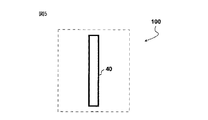
図5に示すように、流体ダクト40の断面は、実質的な矩形であってもよい。流体ダクト40の隅は、丸めてもよい。
As shown in FIG. 5, the cross section of the
図6に示すように、シャッター100は、動作速度を速くするため、いくつかの隣接した流体ダクト(40a、40b)を備えてもよい。このようにすることで、個々の流体最前部は、短い距離のみを移動することで有効領域A1を覆うことができる。第一近似として、動作速度は、流体ダクト(40a、40b)の数に逆比例する。
As shown in FIG. 6, the
例えば、有効領域D1の幅を5mmにして、シャッター100は、17個の流体ダクト(40a、40b)を備えてもよい。個々の流体ダクト40の幅D4は、0.1mmにして、隣接するダクトの間隔は、0.2mmとする。この場合、有効領域の全幅A1は、34個(=2×17)の流体最前部が、横方向に0.1mm移動することにより覆うことができる。従って、流体最前部の速度が10cm/sであれば、切り替え速度は約1msとなる。
For example, the width of the effective area D1 may be 5 mm, and the
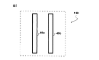
図7のように、隣接する流体ダクト40a、40bは、実質的に矩形の断面を有してもよい。
As shown in FIG. 7,
図8は、流体ダクト40a、40bから発生する第一流体50a、50bの区域が、毛細空間30内で如何に融合するかを示す。第二流体15の同伴(entrainment)を防ぐこと、すなわち流体最前部が互いに合わさる際の気泡の形成を防ぐことが重要である。
FIG. 8 shows how the areas of the first fluid 50 a, 50 b originating from the
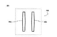
気泡の同伴を防ぐため、図9に示すように、流体ダクト40a、40bの幅を端部より中心部で広くしてもよい。
In order to prevent the entrainment of bubbles, the width of the
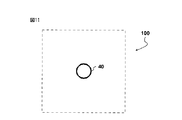
図10に示すように、流体ダクト40の断面は十字型であってもよい。図11に示すように、流体ダクト40の断面は実質的な円形であってもよい。また流体ダクト40の断面は楕円形であってもよい。
As shown in FIG. 10, the cross section of the
図12に示すように、シャッター100は、第一流体50を静電的に移動するための複数の電極5,6を備えてもよい。第一流体50は、第一流体15よりも高い誘電率を有するように選定することができる。この結果、電極5と電極6との間に電圧が印加されると、隣接する電極5と電極6との間に発生する電界が、第一流体50を引き付ける。
As shown in FIG. 12, the
図12は反射状態にあるシャッター100を示す。電極5,6の第二群E2に電圧が印加されると、静電引力が第一流体50を毛細空間30および界面20から引き離し、第一流体50を流体ダクト40a、40bおよび流体容器70に閉じ込める。
FIG. 12 shows the
透明体10は、プリズムであってもよい。シャッター100は、流体ダクト40a、40b、および一つ以上の排気ダクト80を組み込むためのダクト部分92を備えてもよい。毛細空間30の厚さは、スペーサ91によって画定してもよい。流体容器70は、第二スペーサ93と底部94によって組み込んでもよい。
The
図13は、無反射状態にあるシャッター100を示す。静電引力が第一流体50を毛細空間30に引き込むように電極の第一群E1により電界を適用することで、シャッター100は、反射状態から無反射状態に変えることができる。電極の第二群E2に印加された電位差は、それぞれスイッチオフされる。
FIG. 13 shows the
電極配列E2に電圧を印加し、電極配列E1を電圧から切り離すことにより、シャッター100を反射状態に再度設定することができる。
By applying a voltage to the electrode array E2 and disconnecting the electrode array E1 from the voltage, the
一定の電位差、パルス電位差、または交流電位差を、電極5,6に印加することができる。印加電圧は、消費電力を節減するためにパルスにしてもよい。電極間の間隔は、例えば100μmにし、電極に印加する電位差は、100から1000Vであれば、これによりそれぞれ1V/μmから10V/μmまでの電界が形成される。電位差および引力は、流体15、50および/または絶縁層の絶縁破壊によって制限される。また電荷トラップと呼ばれる現象により、引力の強さが制限される。電位差は、例えばトランジスターなどの電気的切替装置(図示せず)によって印加することができる。電圧を安定にするため、外部コンデンサーを使用してもよい。低電圧の蓄電池は、昇圧装置によって電圧を高めてもよい。
A constant potential difference, pulse potential difference, or alternating current potential difference can be applied to the
第一流体50は、例えばアルカン(例えばヘキサン)、ケトン類(例えばアセトン、シクロヘキサノン、メチルエチルケトン)またはニトロ誘導体(例えばニトロメタン、ニトロベンゼン、ニトロトルエン)などの炭化水素の中から選定することができる。第一流体50は凍結防止剤を含んでもよい。
The
第二流体15は、誘電透過性の低い気体または液体であってもよい。第二流体は、例えば空気、アルゴンまたは窒素などでもよい。気体の代わりに、例えば、シリコーン油などのような絶縁破壊耐力の高い液体を使用してもよい。
The
また、第一流体50が導電性で、かつ第二流体15が電気絶縁性の場合においても、電界は、第一流体50を引き付ける。この場合、電極5,6と第一流体50との間を絶縁するために、電極5,6は、絶縁層を有する必要がある。第一流体50は、例えば塩化ナトリウム水溶液など導電性の塩溶液であってもよい。
Further, even when the
代わりに、第一流体50を絶縁性とし、第二流体15を導電性としてもよい。
Instead, the
また代わりに、第二流体15は、第一流体30よりも低い屈折率を維持しつつ、誘電率が第一流体50よりも高くなるように選定してもよい。
Alternatively, the
圧力上昇を防ぐために、第二流体15が、排気ダクト80を通じて毛細空間と流体容器70との間を出入りするようにしてもよい。
In order to prevent an increase in pressure, the
排気ダクト80を十分に狭くして、表面張力によって第一流体50が排気ダクト80内に侵入しないようにしてもよい。
The
図14は、第一流体50の一方の側にある複数の電極5,6間において電界を発生させる電極配列を示す模式図である。電極5,6の間に印加された電位差は、第一流体50を引き付ける電界を発生させる。この場合、第一流体50は、比較的高い誘電率を有し、電気的に絶縁性であることが必要である。腐食を抑えるため貴金属電極を使用してもよい。
FIG. 14 is a schematic diagram showing an electrode arrangement for generating an electric field between the plurality of
充填材7は、表面を滑らかにし、電極5と電極6との間を絶縁する。
The
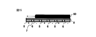
図15は、電極5、6が絶縁層8によって第一流体50から絶縁されている電極配列を示す模式図である。この場合、第一流体50もまた導電性であってもよい。
FIG. 15 is a schematic diagram showing an electrode arrangement in which the
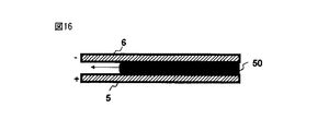
図16は、第一流体50の両側に配置された電極5、6の間において電界を発生させる電極配列を示す模式図である。この場合、第一流体50は、比較的高い誘電率を有し、電気的に絶縁性であることが必要である。
FIG. 16 is a schematic diagram showing an electrode arrangement for generating an electric field between the
また、引力の強さをさらに増大させるために、図14または図15による電極配列を、第一流体50の両側に組み込んでもよい。図12および図13の流体ダクト40a、40bにおいて示すように、第一流体50の反対側の電極は、反対の極性を有するように構成してもよい。
In order to further increase the strength of the attractive force, the electrode arrangement according to FIG. 14 or 15 may be incorporated on both sides of the
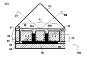
図17は、電極5、6が、絶縁層8によって第一流体50から電気的に絶縁された電極配列を示す模式図である。この場合、第一流体50もまた導電性であってもよい。
FIG. 17 is a schematic diagram showing an electrode arrangement in which the
有効領域A1には、好都合なことに電極構造が無いため、非常に平坦な光学表面が得られる利点がある。しかしながら、いくつかの用途では、界面20の有効領域A1上に透明電極を組み込むことが、有利な場合もある。透明電極は、例えばインジウムスズ酸化物(ITO)などを用いて組み立てることができる。代わりに、メッシュまたは格子状の電極を使用してもよい。
The effective area A1 has the advantage that a very flat optical surface is obtained, since it advantageously has no electrode structure. However, in some applications it may be advantageous to incorporate a transparent electrode on the effective area A1 of the
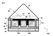
図18は、一つ以上の電極と導電性の第一流体50との間において電界を発生させる電極配列を示す模式図である。言い換えれば、電位差が、一つ以上の電極と第一流体50との間に印加される。
FIG. 18 is a schematic diagram showing an electrode arrangement for generating an electric field between one or more electrodes and the conductive
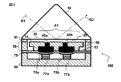
図19に示すように、シャッターは、第一流体50を移動させるために、一つ以上の圧電アクチュエータ(77a、77b)を備えてもよい。膜78およびダクト部分95の空洞が、流体容器70aおよび70bを画定する。
As shown in FIG. 19, the shutter may include one or more piezoelectric actuators (77a, 77b) for moving the
ダクト部分95は、一つ以上の排気ダクト82を備えてもよい。また、ダクト部分95および膜78が、排気容器82を画定する場合もある。毛細空間30の厚さは、スペーサ91によって画定されてもよい。圧電アクチュエータは、底部94によって担持されてもよい。
The
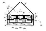
図19は、反射状態にあるシャッター100を示す。図20に示すように、圧電アクチュエータ77a、77bを膨張させることにより、シャッター100を無反射状態に設定することができる。この結果、流体容器70a、70bの内圧が上昇し、第一流体50は毛細空間30に押出され、有効領域A1を覆うことになる。第二流体15を逃がすことは、排気ダクト80を通じて排気容器82へと排出することである。
FIG. 19 shows the
圧電アクチュエータ77a、77bを収縮させることにより、シャッター100は、反射状態に再度設定することができる。この結果、流体容器70a、70b内の圧力は減圧され、第一流体50は、毛細空間30から流体容器70a、70bへと吸引される。
By contracting the
いくつかの流体ダクト40a、40bに対して、共通の流体容器と共通のアクチュエータを使用してもよい。
A common fluid container and a common actuator may be used for several
また、圧電アクチュエータに代わって、別の静電アクチュエータまたは電磁アクチュエータを使用してもよい。電磁アクチュエータは、例えば可動磁石近傍のコイルまたは別のコイルなどに基づくものでよい。静電アクチュエータは、例えば電極近傍で荷電される薄片などに基づくものでよい。 Further, instead of the piezoelectric actuator, another electrostatic actuator or electromagnetic actuator may be used. The electromagnetic actuator may be based on, for example, a coil near the movable magnet or another coil. The electrostatic actuator may be based on a thin piece charged in the vicinity of the electrode, for example.
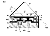
図21に示すように、シャッター100は、第一流体50を有効領域A1内に閉じ込めるために、すなわち第一流体50が排気ダクト80へ逃げるのを防ぐために、電極配列5,6を備えることもできる。言い換えれば、第一流体50の境界を、静電的に安定化させることができる。
As shown in FIG. 21, the
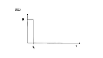
図22は、理想的なシャッターの時間的挙動を示す。Rは反射率を、またtは時間を示す。時刻t0において、コマンドがシャッターに送られると、シャッターの反射率は最大値から直ちに0へと変化する。 FIG. 22 shows the ideal shutter time behavior. R represents reflectance, and t represents time. When a command is sent to the shutter at time t 0 , the reflectance of the shutter immediately changes from the maximum value to 0.
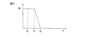
図23に示すように、実際のシャッターは、コマンドの後で何らかの変化が検出されるまで、時間遅れt1‐t0を生じる。反射率の変化は、別の時間間隔t2‐t1の間において起こる。時間間隔t2‐t1は、好都合なことに非常に短く、例えば0.01秒または0.001秒のオーダーなので、露光を正確に画定することになる。 As shown in FIG. 23, the actual shutter produces a time delay t 1 -t 0 until some change is detected after the command. The change in reflectivity occurs during another time interval t 2 -t 1 . The time interval t 2 -t 1 is advantageously very short, for example on the order of 0.01 seconds or 0.001 seconds, so that the exposure is accurately defined.
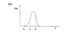
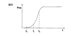
図24は、流体最前部の速度を示し、図25は、流体最前部の位置を時間関数として示す。流体最前部は、t0において動き始める。第一流体50の速度は、時間間隔t1‐t0の間に実質的に加速される。時刻t1において、第一流体50は有効領域に作用する。時刻t2において、第一流体50は有効領域を完全に覆う。時間間隔t2‐t1を最小にするために、第一流体50の最大速度を、時刻t1以前に既に到達させることができ、または、平均速度を、時間間隔t2‐t1の間で最大にすることができる。
FIG. 24 shows the velocity of the fluid front and FIG. 25 shows the position of the fluid front as a function of time. The fluid front starts to move at t 0 . The velocity of the
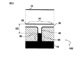
図26に示すように、有効領域A1と流体最前部の初期位置との間の距離D3は、有効領域A1の幅D1の0.5倍以上としてもよい。この間隔D3は、流体最前部が有効領域A1に作用する前に、流体最前部を加速させることを可能にする。間隔D3を増大させることは、シャッターを反射状態から無反射状態に変化させるのに必要な時間間隔t2‐t1を短縮する。しかしながら、距離D3の増大は、遅れt1‐t0に対し不利な影響も及ぼす。従って、距離D3は、用途に応じて選定されるべきである。 As shown in FIG. 26, the distance D3 between the effective area A1 and the initial position of the fluid front part may be 0.5 times or more the width D1 of the effective area A1. This distance D3 makes it possible to accelerate the fluid front before the fluid front acts on the effective area A1. Increasing the interval D3 shortens the time interval t 2 -t 1 required to change the shutter from the reflective state to the non-reflective state. However, increasing the distance D3 also has an adverse effect on the delay t 1 -t 0 . Therefore, the distance D3 should be selected according to the application.
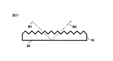
図27に示すように、透明体10は、透明体10内部および/または透明体10外部に光線を連結させるための複数のプリズム突起部を備えてもよい。
As shown in FIG. 27, the
透明体10は、透明体10内に光を連結するための回折格子を備えてもよい。また、透明体10は、透明体10内に光を連結するための傾斜面を備えてもよい。透明体10は、画像光学系300(図1参照)と一体化させることもできる。透明体10は、レンズとして作用する、湾曲、球面、または非球面からなる少なくとも一つの面を有してもよい。一つ以上のレンズを、接着材によって透明体10に固定してもよい。
The
図1に戻り、装置500はデジタルカメラでもよい。また、装置500はデジタルビデオカメラでもよい。また装置500は、画像システムを備える携帯機器でもよい。本装置は、画像システムを備えるモバイル機器でもよい。本装置500は、例えば画像システムを備える携帯電話でもよい。さらに装置500は、画像システムを備えるデータ処理機器でもよい。
Returning to FIG. 1, the
画像センサー200は、感光性画素の配列を備える。例えば電荷結合素子(CCD)技術、または相補型金属酸化物半導体(CMOS)技術を用いて、画像センサー200を組み込むこともできる。また、フォトトランジスタまたはシリコンフォトダイオードを用いて、画像センサー200を組み込んでもよい。
The
被写体900の画像は、
シャッター100を反射状態に設定する工程と、
画像センサー200の実質的な全画素をリセットまたは活性化する工程と、
所定の露光時間の間、画素を露光する工程と、
シャッター100を無反射状態に設定する工程と、
画素から信号をメモリまたは信号処理装置に読み取る工程と、を少なくとも含む方法により得ることができる。
The image of the subject 900 is
Setting the
Resetting or activating substantially all pixels of the
Exposing the pixels for a predetermined exposure time;
Setting the
And reading a signal from the pixel into a memory or a signal processing device.
この場合、無反射状態から反射状態への変化はゆっくり起こるので、シャッター100を開くタイミングは、さほど重要ではない。
In this case, since the change from the non-reflection state to the reflection state occurs slowly, the timing of opening the
代わりに、被写体900の画像は、
画像センサー200の実質的な全画素をリセットまたは活性化する工程と、
シャッター100を反射状態に設定する工程と、
所定の露光時間の間、画素を露光する工程と、
シャッター100を無反射状態に設定する工程と、
画素から信号をメモリまたは信号処理装置に読み取る工程と、を少なくとも含む方法により得ることができる。
Instead, the image of the subject 900 is
Resetting or activating substantially all pixels of the
Setting the
Exposing the pixels for a predetermined exposure time;
Setting the
And reading a signal from the pixel into a memory or a signal processing device.
この場合、シャッター100の開閉動作は、共に重要である。
In this case, both the opening and closing operations of the
原理的には、シャッター100は、画像センサー200への露光開始時のみを制御するのに使用してもよいし、および、露光時間の終了は、必要に応じて別のいくつかの方法で制御を行ってもよい。
In principle, the
当業者にとって、本発明の装置および方法には修正や変形が考えられることは明らかであろう。添付図面を参照しながら上述した特定の実施形態は、説明する目的だけのものあり、添付の請求範囲に定義される本発明の範囲を制限することを意図するものではない。 It will be apparent to those skilled in the art that modifications and variations are possible in the apparatus and method of the present invention. The specific embodiments described above with reference to the accompanying drawings are for illustrative purposes only and are not intended to limit the scope of the invention as defined in the appended claims.
Claims (11)
少なくとも一つの流体容器と、
一定量の流体と、
前記流体容器と前記毛細空間との間で前記流体を移動させ、前記界面の有効領域に作用する傾斜光線の全内部反射を可能とするシャッターの第一動作状態と、前記傾斜光線の前記界面における有効領域を通じた透過を可能とするシャッターの第二動作状態との間で、シャッターの動作状態に変化を起こさせるための流体移動手段と、
前記毛細空間に前記流体を供給するための前記有効領域に対向する一つ以上の流体ダクトと、
前記界面の有効領域を通じて透過する光線を吸収するための吸収手段と、を備える光学シャッター。 An interface between the transparent body and the capillary space;
At least one fluid container;
A certain amount of fluid,
A first operating state of the shutter that moves the fluid between the fluid container and the capillary space and allows total internal reflection of the tilted rays acting on the effective area of the interface; and at the interface of the tilted rays Fluid moving means for causing a change in the operating state of the shutter between the second operating state of the shutter allowing transmission through the effective area;
One or more fluid ducts facing the effective area for supplying the fluid to the capillary space;
And an absorbing means for absorbing light transmitted through the effective area of the interface.
前記光学シャッターは、同様に
透明体と毛細空間との間の界面と、
少なくとも一つの流体容器と、
一定量の流体と、
前記流体容器と前記毛細空間との間で前記流体を移動させ、前記界面の有効領域に作用する傾斜光線の全内部反射を可能とするシャッターの第一動作状態と、前記傾斜光線の前記界面における有効領域を通じた透過を可能とするシャッターの第二動作状態との間で、シャッターの動作状態に変化を起こさせるための流体移動手段と、
前記毛細空間に前記流体を供給するための前記有効領域に対向する一つ以上の流体ダクトと、
前記界面の前記有効領域を通じて透過する光線を吸収するための吸収手段と、を備える光学装置。 An image optical system, an image sensor, and an optical shutter;
Similarly, the optical shutter includes an interface between the transparent body and the capillary space,
At least one fluid container;
A certain amount of fluid,
A first operating state of the shutter that moves the fluid between the fluid container and the capillary space and allows total internal reflection of the tilted rays acting on the effective area of the interface; and at the interface of the tilted rays Fluid moving means for causing a change in the operating state of the shutter between the second operating state of the shutter allowing transmission through the effective area;
One or more fluid ducts facing the effective area for supplying the fluid to the capillary space;
An optical device comprising: absorbing means for absorbing light transmitted through the effective area of the interface.
ある斜角で、前記界面の有効領域に光線を案内すること、
前記界面の有効領域に作用する傾斜光線の全内部反射を可能とする前記シャッターの第一動作状態と、前記傾斜光線の前記界面における有効領域を通じた透過を可能とする前記シャッターの第二動作状態との間で、前記シャッターの動作状態に変化を起こさせるように、前記有効領域に対向する少なくとも一つの流体ダクトにおいて、一つ以上の前記流体ダクトを通じて少なくとも一つの流体容器と前記毛細空間との間で一定量の流体を移動させること、
前記有効領域を透過した光線を吸収すること、および
前記第一動作状態において、前記有効領域から反射された光線を前記画像センサーに案内すること、を備える方法。 A method of controlling exposure of an image sensor by a shutter having an interface between a transparent body and a capillary space,
Guiding light rays to the effective area of the interface at an oblique angle;
A first operating state of the shutter that allows total internal reflection of tilted rays acting on an effective area of the interface; and a second operating state of the shutter that allows transmission of the tilted rays through the effective area at the interface. Between at least one fluid container and the capillary space through one or more fluid ducts in at least one fluid duct facing the effective area so as to cause a change in the operating state of the shutter. Moving a certain amount of fluid between,
Absorbing the light beam transmitted through the effective region; and guiding the light beam reflected from the effective region to the image sensor in the first operating state.
前記画像センサーの画素をリセットまたは活性化する工程と、
前記画素を、所定の露光時間の間、前記反射された光線に露光する工程と、
前記シャッターを前記第二動作状態に設定する工程と、
前記画素から信号をメモリまたは信号処理装置に読み取る工程と、を少なくとも含む、請求項10に記載の方法。 Setting the shutter to the first operating state;
Resetting or activating pixels of the image sensor;
Exposing the pixel to the reflected light beam for a predetermined exposure time;
Setting the shutter to the second operating state;
Reading at least a signal from the pixel into a memory or signal processing device.
Applications Claiming Priority (2)
| Application Number | Priority Date | Filing Date | Title |
|---|---|---|---|
| US11/255,763 | 2005-10-21 | ||
| US11/255,763 US7427745B2 (en) | 2005-10-21 | 2005-10-21 | Optical shutter for miniature cameras |
Related Parent Applications (1)
| Application Number | Title | Priority Date | Filing Date |
|---|---|---|---|
| JP2008536070A Division JP5638757B2 (en) | 2005-10-21 | 2006-10-19 | Optical shutter for miniature cameras |
Publications (1)
| Publication Number | Publication Date |
|---|---|
| JP2013242588A true JP2013242588A (en) | 2013-12-05 |
Family
ID=37962223
Family Applications (2)
| Application Number | Title | Priority Date | Filing Date |
|---|---|---|---|
| JP2008536070A Expired - Fee Related JP5638757B2 (en) | 2005-10-21 | 2006-10-19 | Optical shutter for miniature cameras |
| JP2013149587A Pending JP2013242588A (en) | 2005-10-21 | 2013-07-18 | Optical shutter for miniature camera |
Family Applications Before (1)
| Application Number | Title | Priority Date | Filing Date |
|---|---|---|---|
| JP2008536070A Expired - Fee Related JP5638757B2 (en) | 2005-10-21 | 2006-10-19 | Optical shutter for miniature cameras |
Country Status (7)
| Country | Link |
|---|---|
| US (1) | US7427745B2 (en) |
| EP (2) | EP1946183B1 (en) |
| JP (2) | JP5638757B2 (en) |
| CN (1) | CN101292193B (en) |
| AT (1) | ATE549661T1 (en) |
| ES (1) | ES2384184T3 (en) |
| WO (1) | WO2007045727A1 (en) |
Families Citing this family (20)
| Publication number | Priority date | Publication date | Assignee | Title |
|---|---|---|---|---|
| JP4442580B2 (en) | 2006-03-28 | 2010-03-31 | ソニー株式会社 | Optical element and imaging device |
| US9936143B2 (en) * | 2007-10-31 | 2018-04-03 | Google Technology Holdings LLC | Imager module with electronic shutter |
| KR20130009504A (en) * | 2011-07-15 | 2013-01-23 | 삼성전자주식회사 | Aperture adjustment method and aperture adjustment element |
| US9392322B2 (en) | 2012-05-10 | 2016-07-12 | Google Technology Holdings LLC | Method of visually synchronizing differing camera feeds with common subject |
| US20140071329A1 (en) * | 2012-09-07 | 2014-03-13 | Rambus Inc. | Reconfigurable optical device using a total internal reflection (tir) optical switch |
| KR101939272B1 (en) * | 2013-01-07 | 2019-04-10 | 삼성전자주식회사 | Apparatus for adjusting aperture using microelectrofluidic method |
| KR102100926B1 (en) * | 2013-02-26 | 2020-04-14 | 삼성전자주식회사 | Variable Liquid Device having nonuniform channel and Apparatus included the same |
| EP2887123A1 (en) * | 2013-12-18 | 2015-06-24 | Thomson Licensing | Optical see-through glass type display device and corresponding optical element |
| US9357127B2 (en) | 2014-03-18 | 2016-05-31 | Google Technology Holdings LLC | System for auto-HDR capture decision making |
| US9729784B2 (en) | 2014-05-21 | 2017-08-08 | Google Technology Holdings LLC | Enhanced image capture |
| US9813611B2 (en) | 2014-05-21 | 2017-11-07 | Google Technology Holdings LLC | Enhanced image capture |
| US10250799B2 (en) | 2014-05-21 | 2019-04-02 | Google Technology Holdings LLC | Enhanced image capture |
| US9774779B2 (en) | 2014-05-21 | 2017-09-26 | Google Technology Holdings LLC | Enhanced image capture |
| US9413947B2 (en) | 2014-07-31 | 2016-08-09 | Google Technology Holdings LLC | Capturing images of active subjects according to activity profiles |
| CN105472210A (en) * | 2014-09-12 | 2016-04-06 | 光宝电子(广州)有限公司 | Image capture device |
| US9654700B2 (en) | 2014-09-16 | 2017-05-16 | Google Technology Holdings LLC | Computational camera using fusion of image sensors |
| CN208046758U (en) | 2015-01-30 | 2018-11-02 | 菲力尔系统公司 | Liquid shutter for infrared imaging device and infrared camera |
| US10256121B2 (en) * | 2015-07-06 | 2019-04-09 | Tokyo Electron Limited | Heated stage with variable thermal emissivity method and apparatus |
| US10620380B1 (en) * | 2018-11-02 | 2020-04-14 | Nanning Fugui Precision Industrial Co., Ltd. | Camera module with non-mechanical light-blocking and light-passing function and electronic device using the camera module |
| CN114485946B (en) * | 2020-11-12 | 2023-09-08 | 精工爱普生株式会社 | Color measuring device |
Citations (6)
| Publication number | Priority date | Publication date | Assignee | Title |
|---|---|---|---|---|
| JPH11231373A (en) * | 1998-02-12 | 1999-08-27 | Asahi Optical Co Ltd | Optical diaphragm device |
| JP2001318326A (en) * | 2000-05-12 | 2001-11-16 | Canon Inc | Optical element and two-dimensional image display element constituted by the optical element |
| JP2004144998A (en) * | 2002-10-24 | 2004-05-20 | Hitachi Ltd | Image display device |
| JP2004233798A (en) * | 2003-01-31 | 2004-08-19 | Fuji Photo Film Co Ltd | Display |
| JP2004286825A (en) * | 2003-03-19 | 2004-10-14 | Fuji Photo Film Co Ltd | Flat panel display device |
| JP2005077718A (en) * | 2003-08-29 | 2005-03-24 | Sharp Corp | Interferometric modulator and display device |
Family Cites Families (27)
| Publication number | Priority date | Publication date | Assignee | Title |
|---|---|---|---|---|
| US3614211A (en) * | 1964-01-03 | 1971-10-19 | Bausch & Lomb | Electrically actuated shutter |
| US3614202A (en) * | 1964-01-03 | 1971-10-19 | Bausch & Lomb | Electrically actuated shutter |
| US3614203A (en) * | 1965-06-18 | 1971-10-19 | Bausch & Lomb | High-speed optical shutter |
| US4249814A (en) * | 1979-10-01 | 1981-02-10 | Iowa State University Research Foundation, Inc. | Frustrated total internal reflection camera shutter |
| DE3138968A1 (en) * | 1981-09-30 | 1983-04-14 | Siemens AG, 1000 Berlin und 8000 München | OPTICAL CONTROL DEVICE FOR CONTROLLING THE RADIATION GUIDED IN AN OPTICAL WAVE GUIDE, IN PARTICULAR OPTICAL SWITCHES |
| FR2524658A1 (en) * | 1982-03-30 | 1983-10-07 | Socapex | OPTICAL SWITCH AND SWITCHING MATRIX COMPRISING SUCH SWITCHES |
| US4485405A (en) * | 1982-06-18 | 1984-11-27 | The United States Of America As Represented By The Secretary Of The Navy | Integration time control |
| FR2553907B1 (en) * | 1983-10-21 | 1985-12-13 | Thomson Csf | OPTICAL MODULATOR |
| GB2206977A (en) | 1987-07-14 | 1989-01-18 | Gen Electric Conpany Plc The | Integrated optical switch using movable liquid |
| US5184192A (en) * | 1991-07-17 | 1993-02-02 | Millipore Corporation | Photometric apparatus with a flow cell coated with an amorphous fluoropolymer |
| US6559903B2 (en) * | 1991-11-27 | 2003-05-06 | Reveo, Inc. | Non-absorptive electro-optical glazing structure employing composite infrared reflective polarizing filter |
| DE19527566A1 (en) | 1995-07-27 | 1997-01-30 | Sel Alcatel Ag | Optical changeover switch - has channels at light conductor crossings on substrate connected to reservoir containers, one contg. medium with same refractive index as light conductor core, the other a medium with lower refractive index |
| US6377383B1 (en) * | 1997-09-04 | 2002-04-23 | The University Of British Columbia | Optical switching by controllable frustration of total internal reflection |
| US6487333B2 (en) | 1999-12-22 | 2002-11-26 | Agilent Technologies, Inc. | Total internal reflection optical switch |
| JP2002090667A (en) * | 2000-09-13 | 2002-03-27 | Hitachi Cable Ltd | Liquid driven optical switch |
| WO2002039172A2 (en) | 2000-11-13 | 2002-05-16 | Corning Incorporated | Fluidic optical switching elements |
| US6470106B2 (en) * | 2001-01-05 | 2002-10-22 | Hewlett-Packard Company | Thermally induced pressure pulse operated bi-stable optical switch |
| US20030002778A1 (en) | 2001-02-14 | 2003-01-02 | David Bach | Photo-polymer based fiber-optic switch using total internal reflection and micro-fluidic actuation |
| US7016560B2 (en) * | 2001-02-28 | 2006-03-21 | Lightwave Microsystems Corporation | Microfluidic control for waveguide optical switches, variable attenuators, and other optical devices |
| US6949176B2 (en) * | 2001-02-28 | 2005-09-27 | Lightwave Microsystems Corporation | Microfluidic control using dielectric pumping |
| WO2002099527A1 (en) * | 2001-06-05 | 2002-12-12 | Koninklijke Philips Electronics N.V. | Display device based on frustrated total internal reflection |
| US6921175B2 (en) * | 2002-09-19 | 2005-07-26 | Hewlett-Packard Development Company, L.P. | Color-generating device and display system |
| US20040114044A1 (en) * | 2002-12-16 | 2004-06-17 | Mamoto Corporation | Digital camera with keyboard and wireless modem |
| WO2004077819A1 (en) * | 2003-02-25 | 2004-09-10 | Matsushita Electric Industrial Co., Ltd. | Optical sensor |
| US7003204B2 (en) * | 2003-08-07 | 2006-02-21 | Northrop Grumman Corporation | Systems and methods for a continuously variable optical delay line |
| US7410309B2 (en) | 2005-04-06 | 2008-08-12 | Nokia Corporation | Optical shutter |
| JP5176334B2 (en) * | 2007-02-01 | 2013-04-03 | 日亜化学工業株式会社 | Semiconductor light emitting device |
-
2005
- 2005-10-21 US US11/255,763 patent/US7427745B2/en not_active Expired - Lifetime
-
2006
- 2006-10-19 WO PCT/FI2006/050450 patent/WO2007045727A1/en not_active Ceased
- 2006-10-19 AT AT06794166T patent/ATE549661T1/en active
- 2006-10-19 EP EP06794166A patent/EP1946183B1/en not_active Not-in-force
- 2006-10-19 EP EP11187458A patent/EP2423743A1/en not_active Withdrawn
- 2006-10-19 CN CN2006800388538A patent/CN101292193B/en not_active Expired - Fee Related
- 2006-10-19 ES ES06794166T patent/ES2384184T3/en active Active
- 2006-10-19 JP JP2008536070A patent/JP5638757B2/en not_active Expired - Fee Related
-
2013
- 2013-07-18 JP JP2013149587A patent/JP2013242588A/en active Pending
Patent Citations (6)
| Publication number | Priority date | Publication date | Assignee | Title |
|---|---|---|---|---|
| JPH11231373A (en) * | 1998-02-12 | 1999-08-27 | Asahi Optical Co Ltd | Optical diaphragm device |
| JP2001318326A (en) * | 2000-05-12 | 2001-11-16 | Canon Inc | Optical element and two-dimensional image display element constituted by the optical element |
| JP2004144998A (en) * | 2002-10-24 | 2004-05-20 | Hitachi Ltd | Image display device |
| JP2004233798A (en) * | 2003-01-31 | 2004-08-19 | Fuji Photo Film Co Ltd | Display |
| JP2004286825A (en) * | 2003-03-19 | 2004-10-14 | Fuji Photo Film Co Ltd | Flat panel display device |
| JP2005077718A (en) * | 2003-08-29 | 2005-03-24 | Sharp Corp | Interferometric modulator and display device |
Also Published As
| Publication number | Publication date |
|---|---|
| CN101292193A (en) | 2008-10-22 |
| ES2384184T3 (en) | 2012-07-02 |
| ATE549661T1 (en) | 2012-03-15 |
| US20070090283A1 (en) | 2007-04-26 |
| JP2009512889A (en) | 2009-03-26 |
| US7427745B2 (en) | 2008-09-23 |
| EP1946183A1 (en) | 2008-07-23 |
| JP5638757B2 (en) | 2014-12-10 |
| CN101292193B (en) | 2011-05-18 |
| EP2423743A1 (en) | 2012-02-29 |
| EP1946183A4 (en) | 2009-08-19 |
| EP1946183B1 (en) | 2012-03-14 |
| WO2007045727A1 (en) | 2007-04-26 |
Similar Documents
| Publication | Publication Date | Title |
|---|---|---|
| JP5638757B2 (en) | Optical shutter for miniature cameras | |
| US6702483B2 (en) | Optical element | |
| US8488249B2 (en) | Optical element, imaging device, and method of driving the optical element | |
| CN100520450C (en) | Optical element | |
| US7764436B2 (en) | Device and method to realize a light processor | |
| US8059343B2 (en) | Optical element and imaging device | |
| JP4424708B2 (en) | Optical system and photographing apparatus incorporating optical element, aperture or shutter in lens element | |
| TW200533953A (en) | Zoom optical system | |
| US20070007849A1 (en) | Small thin film-movable element, small thin film-movable element array and image forming apparatus | |
| JP2002162506A (en) | Optical element, optical device and photographing device | |
| CN103038672A (en) | Reconfigurable, non-oscillating liquid lens and imaging system | |
| JP4442580B2 (en) | Optical element and imaging device | |
| WO2020019838A1 (en) | Imaging module, camera assembly and electronic device | |
| US7410309B2 (en) | Optical shutter | |
| JP2008175918A (en) | Optical element, photographing optical system, imaging method and photographing method | |
| CN100443927C (en) | Liquid-based optical device, method for controlling such device, and electronic device | |
| JP2003057409A (en) | Optical element and optical equipment | |
| HK1163831A (en) | Optical shutter for miniature cameras | |
| JP4471036B2 (en) | Shutter device and imaging device | |
| KR100636433B1 (en) | Lens elements | |
| CN115469386B (en) | Liquid lens and camera module | |
| KR100752012B1 (en) | Camera module for mobile terminal | |
| JP2006243674A (en) | Optical element and optical apparatus | |
| JP2006235549A (en) | Lens barrel, lens barrel unit and imaging apparatus | |
| WO2018076153A1 (en) | Gas lens |
Legal Events
| Date | Code | Title | Description |
|---|---|---|---|
| A977 | Report on retrieval |
Free format text: JAPANESE INTERMEDIATE CODE: A971007 Effective date: 20140630 |
|
| A131 | Notification of reasons for refusal |
Free format text: JAPANESE INTERMEDIATE CODE: A131 Effective date: 20140701 |
|
| A521 | Request for written amendment filed |
Free format text: JAPANESE INTERMEDIATE CODE: A523 Effective date: 20141001 |
|
| RD03 | Notification of appointment of power of attorney |
Free format text: JAPANESE INTERMEDIATE CODE: A7423 Effective date: 20141203 |
|
| RD04 | Notification of resignation of power of attorney |
Free format text: JAPANESE INTERMEDIATE CODE: A7424 Effective date: 20150213 |
|
| A02 | Decision of refusal |
Free format text: JAPANESE INTERMEDIATE CODE: A02 Effective date: 20150331 |
|
| RD04 | Notification of resignation of power of attorney |
Free format text: JAPANESE INTERMEDIATE CODE: A7424 Effective date: 20150428 |