JP2013247252A - 炭化珪素半導体装置およびその製造方法 - Google Patents
炭化珪素半導体装置およびその製造方法 Download PDFInfo
- Publication number
- JP2013247252A JP2013247252A JP2012120263A JP2012120263A JP2013247252A JP 2013247252 A JP2013247252 A JP 2013247252A JP 2012120263 A JP2012120263 A JP 2012120263A JP 2012120263 A JP2012120263 A JP 2012120263A JP 2013247252 A JP2013247252 A JP 2013247252A
- Authority
- JP
- Japan
- Prior art keywords
- layer
- conductivity type
- type semiconductor
- semiconductor device
- silicon carbide
- Prior art date
- Legal status (The legal status is an assumption and is not a legal conclusion. Google has not performed a legal analysis and makes no representation as to the accuracy of the status listed.)
- Granted
Links
Images






Classifications
-
- H—ELECTRICITY
- H10—SEMICONDUCTOR DEVICES; ELECTRIC SOLID-STATE DEVICES NOT OTHERWISE PROVIDED FOR
- H10D—INORGANIC ELECTRIC SEMICONDUCTOR DEVICES
- H10D30/00—Field-effect transistors [FET]
- H10D30/60—Insulated-gate field-effect transistors [IGFET]
- H10D30/64—Double-diffused metal-oxide semiconductor [DMOS] FETs
- H10D30/66—Vertical DMOS [VDMOS] FETs
-
- H—ELECTRICITY
- H10—SEMICONDUCTOR DEVICES; ELECTRIC SOLID-STATE DEVICES NOT OTHERWISE PROVIDED FOR
- H10D—INORGANIC ELECTRIC SEMICONDUCTOR DEVICES
- H10D12/00—Bipolar devices controlled by the field effect, e.g. insulated-gate bipolar transistors [IGBT]
- H10D12/01—Manufacture or treatment
-
- H—ELECTRICITY
- H10—SEMICONDUCTOR DEVICES; ELECTRIC SOLID-STATE DEVICES NOT OTHERWISE PROVIDED FOR
- H10D—INORGANIC ELECTRIC SEMICONDUCTOR DEVICES
- H10D12/00—Bipolar devices controlled by the field effect, e.g. insulated-gate bipolar transistors [IGBT]
- H10D12/01—Manufacture or treatment
- H10D12/031—Manufacture or treatment of IGBTs
-
- H—ELECTRICITY
- H10—SEMICONDUCTOR DEVICES; ELECTRIC SOLID-STATE DEVICES NOT OTHERWISE PROVIDED FOR
- H10D—INORGANIC ELECTRIC SEMICONDUCTOR DEVICES
- H10D12/00—Bipolar devices controlled by the field effect, e.g. insulated-gate bipolar transistors [IGBT]
- H10D12/411—Insulated-gate bipolar transistors [IGBT]
- H10D12/441—Vertical IGBTs
-
- H—ELECTRICITY
- H10—SEMICONDUCTOR DEVICES; ELECTRIC SOLID-STATE DEVICES NOT OTHERWISE PROVIDED FOR
- H10D—INORGANIC ELECTRIC SEMICONDUCTOR DEVICES
- H10D30/00—Field-effect transistors [FET]
- H10D30/01—Manufacture or treatment
- H10D30/021—Manufacture or treatment of FETs having insulated gates [IGFET]
- H10D30/028—Manufacture or treatment of FETs having insulated gates [IGFET] of double-diffused metal oxide semiconductor [DMOS] FETs
- H10D30/0291—Manufacture or treatment of FETs having insulated gates [IGFET] of double-diffused metal oxide semiconductor [DMOS] FETs of vertical DMOS [VDMOS] FETs
-
- H—ELECTRICITY
- H10—SEMICONDUCTOR DEVICES; ELECTRIC SOLID-STATE DEVICES NOT OTHERWISE PROVIDED FOR
- H10D—INORGANIC ELECTRIC SEMICONDUCTOR DEVICES
- H10D62/00—Semiconductor bodies, or regions thereof, of devices having potential barriers
- H10D62/10—Shapes, relative sizes or dispositions of the regions of the semiconductor bodies; Shapes of the semiconductor bodies
- H10D62/124—Shapes, relative sizes or dispositions of the regions of semiconductor bodies or of junctions between the regions
- H10D62/126—Top-view geometrical layouts of the regions or the junctions
- H10D62/127—Top-view geometrical layouts of the regions or the junctions of cellular field-effect devices, e.g. multicellular DMOS transistors or IGBTs
-
- H—ELECTRICITY
- H10—SEMICONDUCTOR DEVICES; ELECTRIC SOLID-STATE DEVICES NOT OTHERWISE PROVIDED FOR
- H10D—INORGANIC ELECTRIC SEMICONDUCTOR DEVICES
- H10D62/00—Semiconductor bodies, or regions thereof, of devices having potential barriers
- H10D62/10—Shapes, relative sizes or dispositions of the regions of the semiconductor bodies; Shapes of the semiconductor bodies
- H10D62/17—Semiconductor regions connected to electrodes not carrying current to be rectified, amplified or switched, e.g. channel regions
- H10D62/393—Body regions of DMOS transistors or IGBTs
-
- H—ELECTRICITY
- H10—SEMICONDUCTOR DEVICES; ELECTRIC SOLID-STATE DEVICES NOT OTHERWISE PROVIDED FOR
- H10D—INORGANIC ELECTRIC SEMICONDUCTOR DEVICES
- H10D62/00—Semiconductor bodies, or regions thereof, of devices having potential barriers
- H10D62/40—Crystalline structures
- H10D62/405—Orientations of crystalline planes
-
- H—ELECTRICITY
- H10—SEMICONDUCTOR DEVICES; ELECTRIC SOLID-STATE DEVICES NOT OTHERWISE PROVIDED FOR
- H10D—INORGANIC ELECTRIC SEMICONDUCTOR DEVICES
- H10D62/00—Semiconductor bodies, or regions thereof, of devices having potential barriers
- H10D62/80—Semiconductor bodies, or regions thereof, of devices having potential barriers characterised by the materials
- H10D62/83—Semiconductor bodies, or regions thereof, of devices having potential barriers characterised by the materials being Group IV materials, e.g. B-doped Si or undoped Ge
- H10D62/832—Semiconductor bodies, or regions thereof, of devices having potential barriers characterised by the materials being Group IV materials, e.g. B-doped Si or undoped Ge being Group IV materials comprising two or more elements, e.g. SiGe
- H10D62/8325—Silicon carbide
-
- H—ELECTRICITY
- H10—SEMICONDUCTOR DEVICES; ELECTRIC SOLID-STATE DEVICES NOT OTHERWISE PROVIDED FOR
- H10D—INORGANIC ELECTRIC SEMICONDUCTOR DEVICES
- H10D64/00—Electrodes of devices having potential barriers
- H10D64/20—Electrodes characterised by their shapes, relative sizes or dispositions
- H10D64/27—Electrodes not carrying the current to be rectified, amplified, oscillated or switched, e.g. gates
- H10D64/311—Gate electrodes for field-effect devices
- H10D64/411—Gate electrodes for field-effect devices for FETs
- H10D64/511—Gate electrodes for field-effect devices for FETs for IGFETs
- H10D64/517—Gate electrodes for field-effect devices for FETs for IGFETs characterised by the conducting layers
- H10D64/519—Gate electrodes for field-effect devices for FETs for IGFETs characterised by the conducting layers characterised by their top-view geometrical layouts
-
- H—ELECTRICITY
- H10—SEMICONDUCTOR DEVICES; ELECTRIC SOLID-STATE DEVICES NOT OTHERWISE PROVIDED FOR
- H10P—GENERIC PROCESSES OR APPARATUS FOR THE MANUFACTURE OR TREATMENT OF DEVICES COVERED BY CLASS H10
- H10P30/00—Ion implantation into wafers, substrates or parts of devices
- H10P30/20—Ion implantation into wafers, substrates or parts of devices into semiconductor materials, e.g. for doping
- H10P30/202—Ion implantation into wafers, substrates or parts of devices into semiconductor materials, e.g. for doping characterised by the semiconductor materials
- H10P30/204—Ion implantation into wafers, substrates or parts of devices into semiconductor materials, e.g. for doping characterised by the semiconductor materials into Group IV semiconductors
- H10P30/2042—Ion implantation into wafers, substrates or parts of devices into semiconductor materials, e.g. for doping characterised by the semiconductor materials into Group IV semiconductors into crystalline silicon carbide
-
- H—ELECTRICITY
- H10—SEMICONDUCTOR DEVICES; ELECTRIC SOLID-STATE DEVICES NOT OTHERWISE PROVIDED FOR
- H10P—GENERIC PROCESSES OR APPARATUS FOR THE MANUFACTURE OR TREATMENT OF DEVICES COVERED BY CLASS H10
- H10P30/00—Ion implantation into wafers, substrates or parts of devices
- H10P30/20—Ion implantation into wafers, substrates or parts of devices into semiconductor materials, e.g. for doping
- H10P30/21—Ion implantation into wafers, substrates or parts of devices into semiconductor materials, e.g. for doping of electrically active species
-
- H—ELECTRICITY
- H10—SEMICONDUCTOR DEVICES; ELECTRIC SOLID-STATE DEVICES NOT OTHERWISE PROVIDED FOR
- H10P—GENERIC PROCESSES OR APPARATUS FOR THE MANUFACTURE OR TREATMENT OF DEVICES COVERED BY CLASS H10
- H10P30/00—Ion implantation into wafers, substrates or parts of devices
- H10P30/20—Ion implantation into wafers, substrates or parts of devices into semiconductor materials, e.g. for doping
- H10P30/28—Ion implantation into wafers, substrates or parts of devices into semiconductor materials, e.g. for doping characterised by an annealing step, e.g. for activation of dopants
-
- H—ELECTRICITY
- H10—SEMICONDUCTOR DEVICES; ELECTRIC SOLID-STATE DEVICES NOT OTHERWISE PROVIDED FOR
- H10D—INORGANIC ELECTRIC SEMICONDUCTOR DEVICES
- H10D62/00—Semiconductor bodies, or regions thereof, of devices having potential barriers
- H10D62/10—Shapes, relative sizes or dispositions of the regions of the semiconductor bodies; Shapes of the semiconductor bodies
- H10D62/102—Constructional design considerations for preventing surface leakage or controlling electric field concentration
- H10D62/103—Constructional design considerations for preventing surface leakage or controlling electric field concentration for increasing or controlling the breakdown voltage of reverse-biased devices
- H10D62/105—Constructional design considerations for preventing surface leakage or controlling electric field concentration for increasing or controlling the breakdown voltage of reverse-biased devices by having particular doping profiles, shapes or arrangements of PN junctions; by having supplementary regions, e.g. junction termination extension [JTE]
- H10D62/109—Reduced surface field [RESURF] PN junction structures
- H10D62/111—Multiple RESURF structures, e.g. double RESURF or 3D-RESURF structures
Landscapes
- Electrodes Of Semiconductors (AREA)
- Insulated Gate Type Field-Effect Transistor (AREA)
Abstract
【解決手段】炭化珪素半導体装置は、第1導電型の半導体基板1と、半導体基板1上に形成された低不純物濃度の第1導電型の半導体層2と、第1導電型の半導体層2に選択的に形成された高不純物濃度の第2導電型の半導体層3と、第2導電型の半導体層3の表面に形成された低不純物濃度の第2導電型のベース層4と、ベース層4の表面層に選択的に形成された第1導電型のソース領域7と、表面からベース層4を貫通して第1導電型の半導体層2に達するように形成された第1導電型のウェル領域6と、ソース領域7とウェル領域6とに挟まれたベース層4の表面にゲート絶縁膜を介して形成されたゲート電極9とを有する。そして、異なるセルのそれぞれの第2導電型の半導体層3の一部同士を、ウェル領域6の下の領域で互いに結合部3aにより結合させる。
【選択図】図1
Description
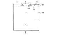
図1は、本発明の第1実施例のSiC−MOSFETの製造工程を示す断面図である。図1の(a)はp+層が結合していない部分の断面図、(b)は、p+層が結合している部分の断面図である。
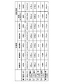
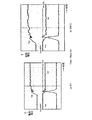
本発明の実施例2では、実施例1と同様の製造工程にて1200V、25AのSiC−MOSFETを作成した。この実施例2ではn型半導体基板1の結晶学的面指数は(0001)面に対して4度傾いた面の上に、窒素を1.8×1016cm-3程度含むn型SiC層2を10μm程度エピタキシャル成長させている。その他の工程、およびセル構造は全く同一である。実施例2の素子の電気特性評価結果は、上記図3に示されており、オン抵抗は、実施例1に対し、55%ほど増加するが、通常のSiC−MOSFETに対しては十分低いオン抵抗特性を示していることがわかる。なお、n型半導体基板1の結晶学的面指数は(0001)面に対して0度、2度、8度、10度傾いた面上に、n型SiC層2を同様に成膜し、作成した素子についても素子評価を行ったところ、特性の変化はほとんどなく良好であった。
本発明の実施例3では、実施例1と同様の製造工程にて1200V、25AのSiC−MOSFETを作製した。n型半導体基板1の結晶学的面指数は(000−1)面に対して4度傾いた面の上に窒素を1.8×1016cm-3程度含むn型SiC層2を10μm程度エピタキシャル成長させている。
本発明の実施例4の製造方法について説明する。まず、n型のSiC半導体基板1を用意する。不純物として窒素を2×1019cm-3程度含む低抵抗のSiC半導体基板1を用いた。次に、n型半導体基板1の結晶学的面指数は(000−1)面に対して4度傾いた面の上に窒素を1.8×1016cm-3程度含むn型SiC層2を10μm程度エピタキシャル成長させる。つぎに、n型SiC層2の上に幅13μm、厚さ0.5μmのp+層3をエピタキシャル法で形成する。その際の不純物イオンにアルミニウムを用いた。また、不純物濃度は、1.0×1018cm-3となるようにドーズ量を設定した。その際、実施例1と同様、n打ち返し層6の下でp+層3の一部を互いに結合するようにする(図2参照)。実施例4では、6角形セルパターンにて作成したが、4角形セルなどでも問題ない。また、p+層3間において結合していない箇所のp+層3間の距離は2μmとした。
実施例5では、実施例4と同様の製造工程にて1200V、25AのSiC−MOSFETを作製した。ただし、実施例5では、n型半導体基板1の結晶学的面指数は(0001)面に対して4度傾いた面の上に窒素を1.8×1016cm-3程度含むn型SiC層2を10μm程度エピタキシャル成長させた。その他の工程は全く同一である。作製した素子の電気特性評価結果を図4に示す。オン抵抗は、実施例4に対し、50%ほど増加するものの、通常のSiC−MOSFETに対しては十分低いオン抵抗特性を示していることがわかる。なお、n型半導体基板1の結晶学的面指数は(0001)面に対して0度、2度、8度、10度傾いた面上同様に成膜し、作成した素子についても素子評価を行ったところ、特性の変化はほとんどなく良好であった。
2 SiC層
3 p+層
4 ベース層
6 n打ち返し層
7 ソース層
8 コンタクト層
11 ソース電極
12 裏面電極
20 セル
Claims (9)
- 半導体基板内部に半導体装置構造が作り込まれ、前記半導体装置構造に電気的接触をとるための電極と、外部から前記電極と電気的接触をとるための電極パッドとを備え、前記電極パッドの下部の前記半導体基板にも前記半導体装置構造が作成された炭化珪素半導体装置であって、
前記半導体装置構造は、
第1導電型の半導体基板と、前記半導体基板上に形成された低不純物濃度の第1導電型の半導体層と、前記第1導電型の半導体層に選択的に形成された高不純物濃度の第2導電型の半導体層と、前記第2導電型の半導体層の表面に形成された低不純物濃度の第2導電型のベース層と、前記ベース層の表面層に選択的に形成された第1導電型のソース領域と、表面から前記ベース層を貫通して前記第1導電型の半導体層に達するように形成された第1導電型のウェル領域と、前記ソース領域と前記ウェル領域とに挟まれた前記ベース層の表面にゲート絶縁膜を介して形成された制御電極とを具備し、
異なるセルのそれぞれの前記第2導電型の半導体層の一部同士が、前記ウェル領域の下の領域で互いに結合されていることを特徴とする炭化珪素半導体装置。 - 前記電極パッドがゲートパッドであることを特徴とする請求項1に記載の炭化珪素半導体装置。
- 前記第1導電型の半導体基板の結晶学的面指数は(000−1)面に対して平行な面もしくは10度以内に傾いた面であることを特徴とする請求項1または2に記載の炭化珪素半導体装置。
- 前記第1導電型の半導体基板の結晶学的面指数は(0001)面に対して平行な面もしくは10度以内に傾いた面であることを特徴とする請求項1または2に記載の炭化珪素半導体装置。
- 前記ゲートパッド部分の前記ソース領域が前記ウェル領域によって、前記ゲートパッドの部分以外の前記半導体装置構造のソース領域と電気的に結合されていることを特徴とする請求項1〜4のいずれか一つに記載の炭化珪素半導体装置。
- 前記ソース領域が第2導電型領域に挟まれてなることを特徴とする請求項5に記載の炭化珪素半導体装置。
- 前記ゲートパッド部分の前記ソース領域が直線状に形成されたことを特徴とする請求項5に記載の炭化珪素半導体装置。
- 前記ゲートパッド部分の前記ソース領域が多角形の網の目状に形成されたことを特徴とする請求項5に記載の炭化珪素半導体装置。
- 第1導電型の半導体基板と、前記半導体基板上に形成された低不純物濃度の第1導電型の半導体層と、前記第1導電型の半導体層に選択的に形成された高不純物濃度の第2導電型の半導体層と、前記第2導電型の半導体層の表面に形成された低不純物濃度の第2導電型のベース層と、前記ベース層の表面層に選択的に形成された第1導電型のソース領域と、表面から前記ベース層を貫通して前記第1導電型の半導体層に達するように形成された第1導電型のウェル領域と、前記ソース領域と前記ウェル領域とに挟まれた前記ベース層の表面にゲート絶縁膜を介して形成された制御電極と、を具備し、異なるセルのそれぞれの前記第2導電型の半導体層の一部同士が、前記ウェル領域の下の領域で互いに結合された炭化珪素半導体装置であって、
前記半導体基板上に前記第1導電型の半導体層をエピタキシャル成長により形成し、
前記第1導電型の半導体層の表面に前記第2導電型の半導体層をイオン注入法により選択的に形成し、
前記第1導電型の半導体層と前記第2導電型の半導体層の上に、前記ベース層をエピタキシャル成長法により形成し、
前記ベース層の表面層に前記ソース領域と、表面から前記ベース層を貫通して前記第1導電型の半導体層に達する前記ウェル領域とをイオン注入法により選択的に形成した
ことを特徴とする炭化珪素半導体装置の製造方法。
Priority Applications (3)
| Application Number | Priority Date | Filing Date | Title |
|---|---|---|---|
| JP2012120263A JP6074787B2 (ja) | 2012-05-25 | 2012-05-25 | 炭化珪素半導体装置およびその製造方法 |
| US14/403,422 US9673313B2 (en) | 2012-05-25 | 2013-03-18 | Silicon carbide semiconductor device and fabrication method thereof |
| PCT/JP2013/057746 WO2013175840A1 (ja) | 2012-05-25 | 2013-03-18 | 炭化珪素半導体装置およびその製造方法 |
Applications Claiming Priority (1)
| Application Number | Priority Date | Filing Date | Title |
|---|---|---|---|
| JP2012120263A JP6074787B2 (ja) | 2012-05-25 | 2012-05-25 | 炭化珪素半導体装置およびその製造方法 |
Publications (2)
| Publication Number | Publication Date |
|---|---|
| JP2013247252A true JP2013247252A (ja) | 2013-12-09 |
| JP6074787B2 JP6074787B2 (ja) | 2017-02-08 |
Family
ID=49623544
Family Applications (1)
| Application Number | Title | Priority Date | Filing Date |
|---|---|---|---|
| JP2012120263A Active JP6074787B2 (ja) | 2012-05-25 | 2012-05-25 | 炭化珪素半導体装置およびその製造方法 |
Country Status (3)
| Country | Link |
|---|---|
| US (1) | US9673313B2 (ja) |
| JP (1) | JP6074787B2 (ja) |
| WO (1) | WO2013175840A1 (ja) |
Cited By (10)
| Publication number | Priority date | Publication date | Assignee | Title |
|---|---|---|---|---|
| JP2016004966A (ja) * | 2014-06-19 | 2016-01-12 | 富士電機株式会社 | 半導体装置および半導体装置の製造方法 |
| JP2016025336A (ja) * | 2014-07-24 | 2016-02-08 | 富士電機株式会社 | 半導体装置及び半導体装置の製造方法 |
| JP2016029707A (ja) * | 2014-07-24 | 2016-03-03 | 住友電気工業株式会社 | 炭化珪素半導体装置 |
| DE102015214797A1 (de) | 2014-09-09 | 2016-03-10 | Sumitomo Electric Industries, Ltd. | Verfahren zur Herstellung einer Siliziumkarbid-Halbleitervorrichtung |
| WO2016039070A1 (ja) * | 2014-09-11 | 2016-03-17 | 富士電機株式会社 | 半導体装置および半導体装置の製造方法 |
| WO2016039071A1 (ja) * | 2014-09-08 | 2016-03-17 | 富士電機株式会社 | 半導体装置及びその製造方法 |
| JP2016048735A (ja) * | 2014-08-27 | 2016-04-07 | 富士電機株式会社 | 半導体装置および半導体装置の製造方法 |
| JP2016058661A (ja) * | 2014-09-11 | 2016-04-21 | 国立研究開発法人産業技術総合研究所 | 半導体装置 |
| WO2017006594A1 (ja) * | 2015-07-08 | 2017-01-12 | 住友電気工業株式会社 | 炭化珪素半導体基板および炭化珪素半導体装置の製造方法 |
| JP2017168677A (ja) * | 2016-03-16 | 2017-09-21 | 富士電機株式会社 | 炭化珪素半導体装置および炭化珪素半導体装置の製造方法 |
Families Citing this family (3)
| Publication number | Priority date | Publication date | Assignee | Title |
|---|---|---|---|---|
| JP6844163B2 (ja) * | 2016-09-14 | 2021-03-17 | 富士電機株式会社 | 炭化珪素半導体装置 |
| JP6903931B2 (ja) * | 2017-02-13 | 2021-07-14 | 富士電機株式会社 | 半導体装置および半導体装置の製造方法 |
| US11075295B2 (en) * | 2018-07-13 | 2021-07-27 | Cree, Inc. | Wide bandgap semiconductor device |
Citations (5)
| Publication number | Priority date | Publication date | Assignee | Title |
|---|---|---|---|---|
| JPH04239137A (ja) * | 1991-01-11 | 1992-08-27 | Nec Corp | 縦型電界効果トランジスタ |
| WO2004036655A1 (ja) * | 2002-10-18 | 2004-04-29 | National Institute Of Advanced Industrial Science And Technology | 炭化ケイ素半導体装置及びその製造方法 |
| JP2009105177A (ja) * | 2007-10-23 | 2009-05-14 | Shindengen Electric Mfg Co Ltd | 半導体装置 |
| JP2010087126A (ja) * | 2008-09-30 | 2010-04-15 | Sanyo Electric Co Ltd | 絶縁ゲート型半導体装置 |
| JP2011258635A (ja) * | 2010-06-07 | 2011-12-22 | Mitsubishi Electric Corp | 半導体装置 |
Family Cites Families (4)
| Publication number | Priority date | Publication date | Assignee | Title |
|---|---|---|---|---|
| JPH08102495A (ja) | 1994-09-30 | 1996-04-16 | Toshiba Corp | 半導体装置 |
| JP4800286B2 (ja) * | 2007-10-16 | 2011-10-26 | Okiセミコンダクタ株式会社 | 半導体装置とその製造方法 |
| JP2010177454A (ja) | 2009-01-29 | 2010-08-12 | Sanyo Electric Co Ltd | 絶縁ゲート型半導体装置 |
| WO2012105611A1 (ja) * | 2011-02-02 | 2012-08-09 | ローム株式会社 | 半導体パワーデバイスおよびその製造方法 |
-
2012
- 2012-05-25 JP JP2012120263A patent/JP6074787B2/ja active Active
-
2013
- 2013-03-18 WO PCT/JP2013/057746 patent/WO2013175840A1/ja not_active Ceased
- 2013-03-18 US US14/403,422 patent/US9673313B2/en active Active
Patent Citations (5)
| Publication number | Priority date | Publication date | Assignee | Title |
|---|---|---|---|---|
| JPH04239137A (ja) * | 1991-01-11 | 1992-08-27 | Nec Corp | 縦型電界効果トランジスタ |
| WO2004036655A1 (ja) * | 2002-10-18 | 2004-04-29 | National Institute Of Advanced Industrial Science And Technology | 炭化ケイ素半導体装置及びその製造方法 |
| JP2009105177A (ja) * | 2007-10-23 | 2009-05-14 | Shindengen Electric Mfg Co Ltd | 半導体装置 |
| JP2010087126A (ja) * | 2008-09-30 | 2010-04-15 | Sanyo Electric Co Ltd | 絶縁ゲート型半導体装置 |
| JP2011258635A (ja) * | 2010-06-07 | 2011-12-22 | Mitsubishi Electric Corp | 半導体装置 |
Cited By (16)
| Publication number | Priority date | Publication date | Assignee | Title |
|---|---|---|---|---|
| JP2016004966A (ja) * | 2014-06-19 | 2016-01-12 | 富士電機株式会社 | 半導体装置および半導体装置の製造方法 |
| JP2016025336A (ja) * | 2014-07-24 | 2016-02-08 | 富士電機株式会社 | 半導体装置及び半導体装置の製造方法 |
| JP2016029707A (ja) * | 2014-07-24 | 2016-03-03 | 住友電気工業株式会社 | 炭化珪素半導体装置 |
| JP2016048735A (ja) * | 2014-08-27 | 2016-04-07 | 富士電機株式会社 | 半導体装置および半導体装置の製造方法 |
| JPWO2016039071A1 (ja) * | 2014-09-08 | 2017-04-27 | 富士電機株式会社 | 半導体装置及びその製造方法 |
| US11239356B2 (en) | 2014-09-08 | 2022-02-01 | Fuji Electric Co., Ltd. | Semiconductor device and method of manufacturing semiconductor device |
| WO2016039071A1 (ja) * | 2014-09-08 | 2016-03-17 | 富士電機株式会社 | 半導体装置及びその製造方法 |
| DE102015214797A1 (de) | 2014-09-09 | 2016-03-10 | Sumitomo Electric Industries, Ltd. | Verfahren zur Herstellung einer Siliziumkarbid-Halbleitervorrichtung |
| JP2016058530A (ja) * | 2014-09-09 | 2016-04-21 | 住友電気工業株式会社 | 炭化珪素半導体装置の製造方法 |
| JP2016058661A (ja) * | 2014-09-11 | 2016-04-21 | 国立研究開発法人産業技術総合研究所 | 半導体装置 |
| JPWO2016039070A1 (ja) * | 2014-09-11 | 2017-04-27 | 富士電機株式会社 | 半導体装置および半導体装置の製造方法 |
| US9960235B2 (en) | 2014-09-11 | 2018-05-01 | Fuji Electric Co., Ltd. | Semiconductor device |
| WO2016039070A1 (ja) * | 2014-09-11 | 2016-03-17 | 富士電機株式会社 | 半導体装置および半導体装置の製造方法 |
| WO2017006594A1 (ja) * | 2015-07-08 | 2017-01-12 | 住友電気工業株式会社 | 炭化珪素半導体基板および炭化珪素半導体装置の製造方法 |
| JPWO2017006594A1 (ja) * | 2015-07-08 | 2018-04-19 | 住友電気工業株式会社 | 炭化珪素半導体基板および炭化珪素半導体装置の製造方法 |
| JP2017168677A (ja) * | 2016-03-16 | 2017-09-21 | 富士電機株式会社 | 炭化珪素半導体装置および炭化珪素半導体装置の製造方法 |
Also Published As
| Publication number | Publication date |
|---|---|
| US20150102363A1 (en) | 2015-04-16 |
| WO2013175840A1 (ja) | 2013-11-28 |
| US9673313B2 (en) | 2017-06-06 |
| JP6074787B2 (ja) | 2017-02-08 |
Similar Documents
| Publication | Publication Date | Title |
|---|---|---|
| JP6074787B2 (ja) | 炭化珪素半導体装置およびその製造方法 | |
| JP5818099B2 (ja) | 半導体装置 | |
| JP6241958B2 (ja) | 高耐圧半導体装置およびその製造方法 | |
| JP5995252B2 (ja) | 縦型高耐圧半導体装置および縦型高耐圧半導体装置の製造方法 | |
| CN104303312B (zh) | 立式耐高压半导体装置及其制造方法 | |
| JP5771678B2 (ja) | 高電力絶縁ゲート・バイポーラ・トランジスタ | |
| JP6183087B2 (ja) | 炭化珪素半導体装置および炭化珪素半導体装置の製造方法 | |
| US8901639B2 (en) | Monolithic bidirectional silicon carbide switching devices | |
| JP2009278067A (ja) | ワイドバンドギャップ半導体装置とその製造方法 | |
| JP2010206002A (ja) | pチャネル型炭化珪素MOSFET | |
| JP6919713B2 (ja) | 炭化珪素半導体装置および炭化珪素半導体装置の製造方法 | |
| JP5939624B2 (ja) | 縦型高耐圧半導体装置の製造方法および縦型高耐圧半導体装置 | |
| JP2018064047A (ja) | 半導体装置および半導体装置の製造方法 | |
| JP7333509B2 (ja) | 炭化珪素半導体装置 |
Legal Events
| Date | Code | Title | Description |
|---|---|---|---|
| A621 | Written request for application examination |
Free format text: JAPANESE INTERMEDIATE CODE: A621 Effective date: 20150522 |
|
| A521 | Request for written amendment filed |
Free format text: JAPANESE INTERMEDIATE CODE: A523 Effective date: 20150515 |
|
| A131 | Notification of reasons for refusal |
Free format text: JAPANESE INTERMEDIATE CODE: A131 Effective date: 20150908 |
|
| A521 | Request for written amendment filed |
Free format text: JAPANESE INTERMEDIATE CODE: A523 Effective date: 20151109 |
|
| A131 | Notification of reasons for refusal |
Free format text: JAPANESE INTERMEDIATE CODE: A131 Effective date: 20160412 |
|
| A521 | Request for written amendment filed |
Free format text: JAPANESE INTERMEDIATE CODE: A523 Effective date: 20160613 |
|
| TRDD | Decision of grant or rejection written | ||
| A01 | Written decision to grant a patent or to grant a registration (utility model) |
Free format text: JAPANESE INTERMEDIATE CODE: A01 Effective date: 20161122 |
|
| A61 | First payment of annual fees (during grant procedure) |
Free format text: JAPANESE INTERMEDIATE CODE: A61 Effective date: 20161221 |
|
| R150 | Certificate of patent or registration of utility model |
Ref document number: 6074787 Country of ref document: JP Free format text: JAPANESE INTERMEDIATE CODE: R150 |
|
| R250 | Receipt of annual fees |
Free format text: JAPANESE INTERMEDIATE CODE: R250 |
|
| R250 | Receipt of annual fees |
Free format text: JAPANESE INTERMEDIATE CODE: R250 |
|
| R250 | Receipt of annual fees |
Free format text: JAPANESE INTERMEDIATE CODE: R250 |
|
| R250 | Receipt of annual fees |
Free format text: JAPANESE INTERMEDIATE CODE: R250 |
|
| R250 | Receipt of annual fees |
Free format text: JAPANESE INTERMEDIATE CODE: R250 |
|
| R250 | Receipt of annual fees |
Free format text: JAPANESE INTERMEDIATE CODE: R250 |
|
| R250 | Receipt of annual fees |
Free format text: JAPANESE INTERMEDIATE CODE: R250 |